vi
ABSTRACT
vii
ABSTRAK
viii
TABLE OF CONTENTS
CONTENTS PAGE
TITTLE i
STATUS VERIFICATION FORM ii
STUDENT DECLARATION iii
SUPERVISOR DECLARATION iv
ACKNOWLEDGEMENT v
ABSTRACT vi
ABSTRAK vii
LIST OF TABLES xi
LIST OF FIGURES xii
LIST OF ABBREVIATIONS xvi
LIST OF APPENDICES xviii
CHAPTER 1: INTRODUCTION 1
1.1 Project Background 1
1.1.1 Transducer (Antenna) 2
1.1.2 Power conversion (Rectifier) 3
1.1.3 Power management 3
1.1.4 Charge storage 3
1.2 Problem Statement 5
1.3 Objectives 6
1.4 Scope of Works 6
CHAPTER 2: LITERATURE REVIEW 7
2 Overview 7
2.1 DC analysis for MOSFET circuits 7
2.1.1 Cut-off 8
ix
2.1.3 Saturation 8
2.2 Energy efficiency of power management system 9
2.3 Power Management System 11
2.3.1 Energy Management System 11
2.3.2 Maximum Power Point 12
2.3.3 Energy-Adaptive MPPT 12
2.4 MPPT techniques 17
2.4.1 Perturbation and Observation (P&O) 18
2.4.2 Fractional Open Circuit Voltage (FOCV) 18
2.5 Summary of Chapter 19
CHAPTER 3: METHODOLOGY 20
3 Overview 20
3.1 Custom Design Flow 21
3.1.1 Project Design Flow 22
3.1.2 Design Comparison 23
3.1.3 Design Specification 23
3.1.4 Design Strategies 24
3.2 Schematic Design 25
3.3 Layout Design 26
3.4 Design Rule Check (DRC) 26
3.5 Layout versus Schematic (LVS) 27
3.6 Layout Parasitic Extraction (LPE or PEX) 28
3.7 Simulation of Extracted Netlist 29
3.8 Summary of Chapter 30
CHAPTER 5: RESULT AND SIMULATION 31
4 Overview 31
x
4.2 MPPT Decision Making Circuit 38
4.2.1 MPPT Algorithm (Analog) 39
4.2.2 Multiplier 40
4.2.3 Sample and Hold Circuit 43
4.2.4 Comparator 44
4.2.5 D Flip-Flop 46
4.2.6 XNOR Gate 47
4.2.7 Simulation Result and Discussion 49
4.3 Parametric Optimization and Layout Design 52
4.3.1 Parametric Optimization 52
4.3.2 Layout Design 55
4.4 Digital Controlled MPPT by microcontroller 59
4.4.1 MPPT Algorithm (Digital) 59
4.4.2 Operation modes of circuit 60
4.4.2 Prototype using Arduino as microcontroller unit 62 4.4.3 Serial Monitor Print and Serial Plotter Print 63
4.5 Summary of Chapter 64
CHAPTER 5: CONCLUSION 65
5 Introduction 65
5.1 Sustainability and Commercialization 65
5.1.1 Sustainability 66
5.1.2 Commercialization 66
5.2 Recommendation and conclusion 67
REFERENCE 68
xi
LIST OF TABLES
Table 4.1: Comparison of Different MPPT Power Management Circuit 33
Table 4.2: Summary of P&O method 47
xii
LIST OF FIGURES
Figure 1.1: The diagram shows the typical energy harvesting sensor 2 application
Figure 1.2: Block Diagram Flow shows steps that harvested energy 4 transfer from Transducer to Load
Figure 2.1: The active full-wave rectifier configuration uses an 14 active diode
Figure 2.2: Schematic of the active diode 14
Figure 2.3: Differential-To-Single ended converter
Figure 2.4: Adaptive charge pump interface comprises the input-load 15 adapting charge pump
Figure 2.5: Comparison of harvesting with the AFW and the ACP 16
Figure 2.6: Schematic of the power management circuit 17
Figure 3.1: Flow chart for custom design process 21
Figure 3.2: Project flow for designing the power management circuit 22
Figure 3.3: Transistor gate width and length, or resistor 24
Figure 3.4: Flow chart for schematic design process 25
Figure 3.5: Layout design example 26
Figure 3.6: Flow chart for design rule check test (DRC) 27
xiii
Figure 3.8: Process of layout and schematic design to extracted netlist 28 using parasitic extraction tool
Figure 3.9: Flow chart for simulation of extracted netlist 29
Figure 3.10: SPICE description and GDSII binary format 29
Figure 4.1: Schematic simulation for common-gate stage active diode 34
Figure 4.2: Input source with cross-coupled transistor rectifier with 35 common-gate stage active diode
Figure 4.3: Self bias stage 35
Figure 4.4: Bias level shifter 36
Figure 4.5: Bias control stage & CG stage 36
Figure 4.6: Switch circuit 37
Figure 4.7: Simulation for common-gate stage active diode at 0.6V 37
Figure 4.8: Simulation for common-gate stage active diode at 3.0V 38
Figure 4.9: Typical MPPT current-voltage-power diagram 38
Figure 4.10: Perturbation and observation algorithm flow chart 39
Figure 4.11: Complete MPPT decision making circuit 40
Figure 4.12: Schematic circuit for multiplier 41
Figure 4.13: Subtractor circuit for multiplier outputs 42
Figure 4.14: Simulation result for multiplier with two analog inputs 42 and the result for the calculator
Figure 4.15: Simulation result for comparison of subtractor with calculator 43 function in software
Figure 4.16: Simple sample and hold circuit 43
Figure 4.17: Sample and hold circuit testband 43
xiv
Figure 4.19: Schematic design for comparator 45
Figure 4.20: Simulation for comparator block 45
Figure 4.21: Simulation result for comparator 45
Figure 4.22: Schematic of D flip-flop using 6 NAND gates 46
Figure 4.23: Simulation for D flip flop block 46
Figure 4.24: Simulation result for D flip flop 47
Figure 4.25: Schematic of XNOR gate 48
Figure 4.26: XNOR gate block testband 49
Figure 4.27: Simulation result for XNOR gate 94
Figure 4.28: Sample timing diagram for MPPT circuit 50
Figure 4.29: Charging stage for simulation result which m is 51 higher than m-1
Figure 4.30: Discharging stage for simulation result which m is 51 higher than m-1
Figure 4.31: Parametric analysis for Lp sweep from 0.5µm to 15µm 52
Figure 4.32: Parametric analysis for Lp (small scale) 53
Figure 4.33: Parametric analysis for comparator circuit width seep 54 from 0.15µm to 20µm
Figure 4.34: Schematic of comparator of analog MPPT circuit 54
Figure 4.35: Typical circuit use for interdigitated transistor 56
Figure 4.36: Configuration of interdigitated pattern 56
Figure 4.37: Dummy transistor 56
Figure 4.38: Typical circuit for common centroid transistor 57
Figure 4.39: Common-centroid pattern used for layout design 57
xv
Figure 4.41: Allocation and arrangement of the transistor in the software 58
Figure 4.42: Complete layout design for the comparator of analog 59 MPPT power management circuit
Figure 4.43: Block diagram for digital MPPT circuit 60
Figure 4.44: Schematic circuit diagram for digital MPPT circuit 60
Figure 4.45: Operation mode under different voltage conditions for 62 the MPPT circuit
Figure 4.46: Prototype of digital MPPT circuit 62
Figure 4.47: Serial monitor printing for the results of digital MPPT 63 circuit
xvi
LIST OF ABBREVIATIONS
RF - Radio Frequency 1
IoT - Internet of Things 5
MPPT - Maximum Power Point Tracking 5
DRC - Design Rule Check 6
LVS - Layout Versus Schematic 6
PEX - Practices Extraction 6
GDSII - Graphic Database System Stream Format File 6
MOSFET - Metal-Oxide-Semiconductor-Field-Effect Transistor 7
CMOS - Complementary Metal-Oxide Semiconductor 9
DSP - Digital Signal Processor 13
MPP - Maximum Power Point 13
P&O - Perturbation and Observation 17
FOCV - Fractional Open Circuit Voltage 17
DTCM - Design Time Component Matching 17
P-MOS - P-Type Metal-Oxide Semiconductor 32
N-MOS - N-Type Metal-Oxide Semiconductor 32
PMC - Power Management Circuit 32
xvii
Lp - Length of P-Type Transistor 35
Wn - Width of N-Type Transistor 35
Ln - Length of N-Type Transistor 35
m-1 - Current Perturbation 49
m - Next Perturbation 49
clk - Clock Signal 49
cmd - Comparator Output 49
Q1 - First Flip Flop Output 49
Q2 - Second Flip Flop 49
MCU - Microcontroller Unit 59
PWM - Pulse Width Modulation 64
DfE - Design for Environment 66
xviii
LIST OF APPENDICES
APPENDIX A - Energy Adaptive Power Management System Design using 72 MPPT techniques for energy scavenging in mobile and
wireless devices (Paper to be published)
APPENDIX B - Digitally Controlled MPPT by Arduino Microcontroller 78 using Perturbation and Observation Algorithm
(Paper to be published)
APPENDIX C - Design and Parametric Optimization for Comparator in 83 MPPT Decision Making Block
(Paper to be published)
APPENDIX D - INOTEK Poster (Main) 88
1
CHAPTER 1
INTRODUCTION
1.1 Project Background
Several environmental energy sources have been extensively investigated such as light, heat, vibration, and electromagnetic radiation from communication devices. These energy sources able to provide instantaneous power for low power electronics. For example, radio frequency (RF) energy scavenging from wireless electronics system has been widely used in wireless power transmission. In order to optimize the transfer of power into the application devices, an energy-adaptive maximum power point tracking technique is proposed to manage harvested low-level energy from different energy sources.
2
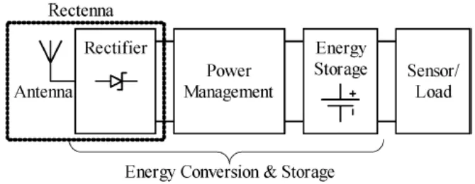
However, the energy harvested by RF harvesting system is still very small. The power management system needs to track the operating voltage which will generate maximum power output for the system in order to maintain the output at a maximum level [1]. In spite of the maximum power generation with power management techniques, the system will not suitable to be implemented when the amount of scavenged energy is small compared to that of consuming energy for the system operation [1]. The diagram below shows the typical energy harvesting sensor application. This paper focuses on the power management block and its interface to the rectenna and energy storage device [2]. In order to optimize the energy harvested, the power management system have to generate maximum output power.
Figure 1.1: The diagram shows the typical energy harvesting sensor application
An energy harvesting system normally included components such as energy harvester or energy transducer, electrical power management or conditioning circuit, energy storage device and electrical load which are applications. The following section will discuss about the components in an energy harvesting system.
1.1.1 Transducer (Antenna)
3
1.1.2 Power conversion (Rectifier)
The power conversion circuit can be a rectifier or DC-DC converter which can converts the provided energy into a suitable DC voltage. In the block diagram, the power conversion is a rectifier which convert RF energy to DC source. The efficiency of the circuit is an important factor which indicates the amount of the useful energy that can be utilized by the application.
1.1.3 Power management
Power conversion circuit usually have different level for available power depending on the application, the output voltage of the power conversion circuit can be regulated to a stable DC voltage using buck or boost converter or it can have limited by voltage limiter. The power management system controls the conduction path between the device and energy harvester. A good power management system can to generate the maximum power output for the energy storage or application devices.
1.1.4 Charge storage
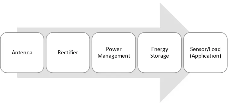
4
Figure 1.2: Block Diagram Flow shows steps that harvested energy transfer from Transducer to Load
Moreover, the system need to be energy adaptive, in order to generate constant outputs despite of the conditions of the harvesting environment changes as periodic changes and other reason, and the result maintains a new operating voltage of maximum power generation. The proposed power management system able to be adaptively manage the harvested energy when different level of voltage is harvest from the sources [2].
Antenna Rectifier Power
Management
Energy Storage
5
1.2 Problem Statement
Energy harvesting has grown from long-established concepts into devices for powering ubiquitously deployed sensor networks and mobile electronics. Systems can scavenge power from human activity or derive limited energy from ambient heat, light, radio, or vibrations. However, if the ubiquitous and sustainable energy sources are not use, the energy source will be a waste to the surrounding. As an example, the RF energy harvesting is developed by the wireless energy transmission technique for harvesting and recycling the ambient RF energy that is widely broadcasted by many wireless systems such as mobile communication systems, Wi-Fi base stations, wireless routers, wireless sensor networks and wireless portable devices. Also, the Internet of things (IoT) is the upcoming technology that will bring the communication between devices to the next level. In other words, IoT means there will be Internet everywhere, and overwhelmed with RF sources. RF energy harvesting is becoming the next generation trend for mobile electronics devices and wireless sensor system. Imagine the mobile devices able to harvesting energy to charge the battery while the user is using the devices or browsing a website by a smartphone. The harvesting will extend and improve the battery life for the devices and sensors without doubts.
6
1.3 Objectives
The objectives of the project included:
To investigate techniques and construct adaptive power management system in miniature size.
To design a power management system to manages low-level energy.
To verify the functionality of the power management system that harvest energy from ubiquitous energy sources in sensor networks and mobile electronics.
1.4 Scope of Works
The project is to design an energy-adaptive MPPT power management unit for harvesting energy from low level power sources. Prior energy sources for the power management system is energy harvested by RF radiation, yet the power management unit will have focused on applications that consume power in the order of µW to mW or even higher in order to implement in more energy scavenging applications. The proposed power management system will manage input voltage sources by energy-adaptive MPPT technique, the energy harvested is able to be manage in high efficiency even when the power level is changed or switched from the harvesting sources.