DESIGN SWITCH MODE POWER SUPPLY BY USING BOOST CONVERTER TOPOLOGY
KHAIRUL IZZAT BIN MOHAMAD SAHIMI
DESIGN SWITCH MODE POWER SUPPLY BY USING BOOST CONVERTER TOPOLOGY
KHAIRUL IZZAT BIN MOHAMAD SAHIMI
This Report Is Submitted In Partial Fulfillment Of Requirements For The Degree of Bachelor In Electrical Engineering (Power Electronic and Drive)
Faculty of Electrical Engineering Universiti Teknikal Malaysia
“I hereby declared that I have read through this report and found that it has comply the partial fulfillment for awarding the degree of Bachelor of Electrical Engineering
(Power Electronic and Drive).”
Signature : ……….
Supervisor’s Name : ……….
“I hereby declared that this report is a result of my own work except for the excerpts that have been cited clearly in the references..”
Signature : ………
Name : ………
Dedicated to :
~ my beloved parents ~
~ my supervisor, En. Fazlli Bin Patkar ~
~ my friends ~
ABSTRACT
ABSTRAK
CONTENTS
CHAPTER TITLE PAGE
TITLE i
DECLARATION ii
DEDICATION iii
ABSTRACT iv
ABSTRAK v
CONTENT vi
LIST OF FIGURE viii
LIST OF NOMENCLATURE x
LIST OF APPENDICES xi
1.0 INTRODUCTION 1
1.1 Objective 1
1.2 Project Scope 2
1.3 Problem Statement 2
2.0 LITERATURE REVIEW
2.1 Power Stage Operation 5
2.2 Feedback Controller Circuit 7
3.0 METHODOLOGY 9
3.1 Literature review on the SMPS. 9 3.2 Design the power stages of SMPS. 9 3.3 Simulate and analyze the circuits with PSpice 9 3.4 Linearization and Small Signal Analysis 10 3.5 Obtain Converter Transfer Function 10
3.6 Open Loop Stability 10
3.7 Design a compensator 10
3.9 The Flow Chart 11
4.0 RESULT AND DISCUSSION 12
4.1 Designing a power stage of SMPS 18
4.2 Linearization 17
4.3 Obtaining Transfer Function 23
4.4 Open Loop Stability 31
4.5 Design a Compensator 34
4.6 Applying Disturbance 41
5.0 CONCLUSION 45
5.1 Discussion 45
5.2 Recommendation 48
5.3 Conclusion 49
REFERENCES 50
APPENDIXES A 51
APPENDIXES B 53
LIST OF FIGURE
N0 TITLE PAGE
2.1 Basic boost converter topology 5 2.2 Current flow through the circuit during ON time 5 2.3 Current flow through the circuit during OFF time 6 2.4 Waveforms of voltage and current during switching operation 6
2.5 Feedback control circuit 7
2.6 Concept of Generated PWM signal 8 4.1 Power stage through a PSpice simulation programme 14
4.2 The output voltage 15
4.3 The output voltage (zoomed in) 15 4.4 Power stage through a PSpice simulation programme 16
4.5 The output voltage 16
4.6 The output voltage (zoomed in) 17
4.7 During switch ON 18
4.8 During switch OFF 19
4.9 Circuit equivalent to the small-signal ac inductor voltage
equation 21
4.10 Circuit equivalent to the small-signal ac capacitor current
equation 22
4.11 The circuit of Figure 4-6, Figure 4-7 collected together 22 4.12 Combination of dependent source into effective ideal transformer,
leading to the final model 23
4.13 A closed loop SMPS block diagram 23
4.14 Generate PWM 24
4.15 Linearization of PWM 24
4.16 A line to output block diagram 26 4.17 A control to output block diagram 26
4.18 set d(s) sources to zero 26
LIST OF FIGURE
N0 TITLE PAGE
4.20 set Vi(s) sources to zero 28
4.21 Push inductor and Vod(s)/D through the transformer 28
4.22 Current Sources set to zero 28
4.23 Voltage source is set to zero 29 4.24 An open loop of SMPS block diagram 31 4.25 Root locus and bode plot of an open loop system 33
4.26 Bode plot of open loop SMPS 33
4.27 Type 3 compensation network 35
4.28 Type 3 compensation algebra on the graph 36 4.29 Adding poles and zero into root locus editor 39 4.30 Gain and Compensator transfer function obtained (red circles) 39 4.31 Bode plot of Uncompesated, Compensated and Compensator
system 40
4.32 Closed loop SMPS with all parameters obtained 41 4.33 Output voltage of closed loop SMPS 41
4.34 Open loop SMPS block diagram 42
4.35 Output voltage of open loop SMPS 42 4.36 An open loop SMPS with a Input Disturbance 43 4.37 Output voltage which disturbance occur at 5th sec 43 4.38 Closed loop SMPS with Input Disturbance 44 4.39 Output voltage which disturbance occur at 5th sec 44 4.40 Output voltage which disturbance occur at 5th sec (zoomed) 44
5.1 SMPS Circuit on PSpice 47
5.2 Output Voltage 47
LIST OF NOMENCLATURE
SMPS Switch Mode Power Supply PSU Power Supply Unit
PWM Pulse Width Modulation DC Direct Current
AC Alternating Current
LIST OF APPENDICES
TITLE PAGE
APPENDIX A 51
APPENDIX B 53
CHAPTER 1
INTRODUCTION
1.1 Objective
The objective of this project is to design, analyze, and control a Switch Mode Power Supply (SMPS) using a boost converter topology. A boost converter is known for its characteristic to amplify or increase the input voltage. The increment of input voltage is being controlled by a switch and a diode instead of a transformer which is widely used in electronic design. The switch and the diode will act by conducting and breaking the flow of current through the circuit and with the additional usage of inductor, it will be able to increase the voltage across the circuit. The inductor characteristic is an element that is able to store energy inside it by charging current through it and also be able to re-use the energy to act as a source in the circuit. A basic circuit of boost converter only is able to increase the voltage without controlling it. The SMPS will be design to be able to maintain its output voltage even with disturbances. This can be done by creating a feedback circuit and applying it into the boost converter circuit
prove that the circuit be able to maintain its output even though there are disturbances with our design. There are many type of electronic simulation programme available in the market but, in this project we will only be using the simulation programme named PSpice so that the designing process will be much easier.
compared with the simulation design because, so that we be able to observe and prove the first objective where the output be able to maintain its value even though there are disturbances. Both of the simulation and the hardware results will be compared so that we be able to recognize the actual error that occurs which affecting the output results that cannot be detected during simulation.
The final objective of this project is that all the designing process and analyzing results will be compiled together making a full guidance in designing a SMPS. The guide will provide a complete step, from the first step of designing an SMPS until the analysis of its output.
1.2 Project Scope
This project focuses primarily on step by step design, analyze and control the switch mode power supply. The design process is a process on designing and theoretically realizing a basic converter topology for SMPS. Meanwhile, the analyzing process is about observing and studying the results of the design’s output. Finally controlling a SMPS is a process where the SMPS will apply a feedback circuit to control its output.
1.3 Problem Statements
CHAPTER 2
LITERATURE REVIEW
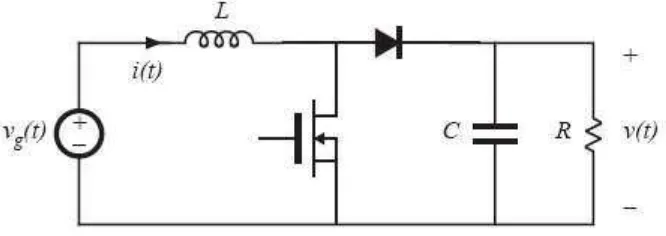
This project is based on designing a SMPS using a boost converter topology which it consist of basic converter that comply with a feedback cicrcuit. A feedback circuit is a controller of the basic converter where it was able to maintain its output due to disturbances. As the SMPS using a boost topology of converter, the circuit will step up the value of input voltage and give a higher output voltage. The circuit consists of high frequency switch, fast recovery diode, inductor and capacitor as shown in Figure 2.1
2.1 Power Stage Operation
[image:20.595.211.407.153.268.2]2.1.1 During Switch ON
Figure 2.2: Current flow through the circuit during ON time
The input voltage will not be directly transferred to the output where at this state, the input voltage will charge up the inductor and store the energy inside. The characteristic of inductor is that it is able to store an energy at a certain capacity depends on its model just like capacitor but instead of voltage, the inductor is charge by current. The output voltage currently will be supplied by the capacitor.
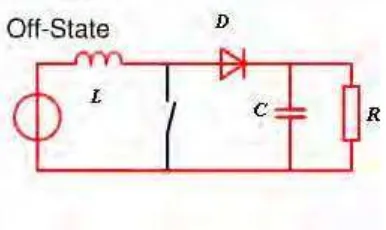
2.1.2 During Switch OFF
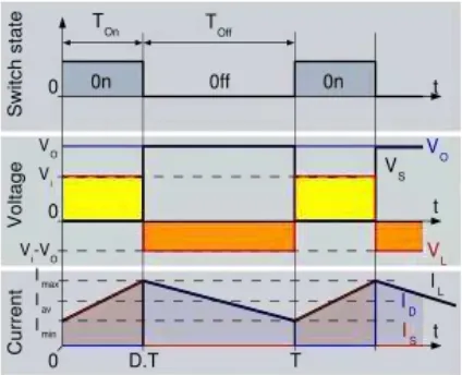
[image:20.595.235.428.599.714.2]The operation of switching resulting a below graphs, where the output voltage is much larger value than the input voltage, and the output current is ramping up and down by the switching sequence.
Figure 2.4: Waveforms of voltage and current during switching operation
As the current is ramping up and down, a ripple is resulted. A large may cause damage to the equipment that is connected to it, so a method of lowering the ripple as much as we could is conducted. We may increase the value of resistor, capacitor or switching frequency to decrease the ripples since the voltage ripple is indirectly proportional to resistor, capacitor, and switching frequency.
D r =
RCf
Then, to control the output voltage, feedback circuit will be applied to the circuit where it will control the switching frequency of the converter and also controlling the duty cycle.
2.2 Feedback Control Circuit
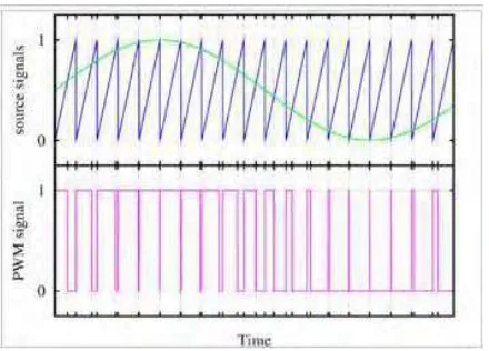
Feedback control circuit consists of Error Amplifier and Pulse Width Modulator, PWM (Figure 2.4). The Error Amplifier acts as a sensor which will sense the output voltage meet the desired voltage or not. A voltage reference shall be set into a comparator and the output of the boost converter shall be connected to it. The comparator shall compare the reference voltage and the output voltage, to sense a
drop or increase in output voltage. If the voltage output does not meet the required voltage, the comparator shall give out a signal or output which acts as an error signal and going into the PWM. The PWM act as a controller to the switching of the MOSFET thus also called as duty cycle
Figure 2.5: Feedback control circuit
[image:23.595.228.448.449.607.2]. The simplest way to generate a PWM signal is the interceptive method, which use 2 type of signal to compare; a saw tooth or a triangle waveform and an error signal. A concept of generated PWM signal is shown in Figure 2.5.
Figure 2.6: Concept of Generated PWM signal