UNIVERSITI TEKNIKAL MALAYSIA MELAKA
Development of Controller for Boost Converter
This report is submitted in accordance with the requirement of the Universiti Teknikal Malaysia Melaka (UTeM) for the Bachelor Degree of Engineering
Technology
(Electronic Industry) (Hons)
By
NUR AFIFI BIN IBRAHIM
B071210157
910727105413
DECLARATION
I hereby, declared this report entitled “Development of Controller for Boost Converter” is the results of my own research except as cited in references.
Signature : ………
Author’s name : NUR AFIFI BIN IBRAHIM
APPROVAL
This report is submitted to the Faculty of Engineering Technology of UTeM as a partial fulfillment of the requirements for the degree of Bachelor of Engineering Technology (Electronic Industry) (Hons.). The member of the supervisory is as follow:
i
ABSTRAK
ii
ABSTRACT
iii
DEDICATION
iv
ACKNOWLEDGEMENT
v
List of abbreviation, symbols and nomenclature xii
CHAPTER 1 1
1.5 Project significant 3
CHAPTER 2 4
LITERATURE REVIEW 4
vi
2.2 DC – DC boost converter 5
2.3 Analysis of DC-DC boost converter 5
2.3.1 Analysis for switch closed 6
2.3.2 Analysis for switch opened 7
2.3.3 General analysis of boost converter condition 8
2.4 Conduction mode of boost converter 9
2.4.1 Continuous conduction mode 9
2.4.2 Discontinuous conduction mode 10
2.5 Pulse width modulation 11
2.6 Control mode of boost converter 11
2.6.1 Voltage control mode 11
2.6.2 Current control mode 12
2.7 Inductance and capacitance value determination 13
2.7.1 Inductance value equation 14
2.7.2 Capacitance value equation 15
2.8 Consideration of diode and electronic switch components 15
2.9 IGBT and MOSFET gate driver 17
2.10 Microcontroller 19
2.10.1 PIC microcontroller 19
vii
CHAPTER 3 21
METHODOLOGY 21
3.1 Introduction 21
3.2 Flow chart of project 22
3.3 Identify problem and do research about project developed 23
3.4 Identify components required 24
3.5 Parameter calculation and circuit simulation 24
3.5.1 Inductance value calculation 25
3.5.2 Capacitance value calculation 25
3.5.3 Simulation software 26
3.5.3.1 PSIM software 27
3.5.3.2 Multisim software 29
3.5.3.4 Proteus software 30
3.6 Microcontroller program code 31
3.7 Hardware development 32
3.8 Test and troubleshoot hardware 32
CHAPTER 4 34
RESULT AND DISCUSSION 34
4.1 Simulation boost converter circuit 34
viii
4.1.3 Output ripple voltage 39
4.1.4 PWM generation from PIC 41
4.2 Hardware development 42
4.2.1 Circuit construction on breadboard 42
4.2.2 Measurement from boost converter 43
4.2.3 MOSFET switching operation 48
4.3 Troubleshoot 49
4.3.1 Re-calculation of inductance and capacitance value 49
4.3.2 Program code modification 51
DC motor voltage range 52
CHAPTER 5 53
CONCLUSION AND FUTURE WORK 53
5.1 Future work 53
5.2 Conclusion 54
APPENDIX A 56
ix
LIST OF FIGURES
2.1 Basic circuit of Boost converter 5
2.2 Condition of Boost converter when switch closed 7
2.3 Condition of Boost converter when switch opened 8
2.4 Inductor voltage and current in CCM 10
2.5 Inductor voltage and current in DCM 10
2.6 Pulse width modulation waveform 11
2.7 Voltage control mode circuit 12
2.8 Current control mode circuit 13
2.9 Electronic switch IGBT 16
2.10 Schottky Diode 16
2.11 Input connection pins 17
2.12 Output connection pins 18
2.13 IGBT and MOSFET Gate Driver 18
2.14 PIC 18F4550 Microcontroller 20
3.1 Flow chart of project 20
3.2 PSIM Interface 26
3.3 SimView Interface 26
3.4 Multisim Interface 27
x
3.6 Proteus Interface for circuit simulation 28
3.7 CCS C Compiler for program coding 29
4.1 Output voltage graph without controller 35
4.2 Analysis of the overshoot percentage, peak time and rise time values 35
4.3 Settling time and final value of graph 36
4.4 Output voltage graph with controller 37
4.5 Analysis of rise time and settling time 38
4.6 The final values of the output voltage graph 38
4.7 Output Voltage Ripple of Boost Converter without Controller 39 4.8: Output Voltage Ripple of Boost Converter with Controller 40
4.9 PWM generated from PIC in PROTEUS 41
4.10: Boost converter circuit on breadboard 42
4.11 The pulse generated from gate driver 43
4.12 The switching process from MOSFET 43
4.13 The input voltage applied to boost converter 44
4.14 The output voltage obtained from the boost converter 44
4.15 The input current flow through circuit 45
4.16: Output current from boost converter 45
4.17 The output voltage from the boost converter 46
xi
LIST OF TABLES
2.1 Absolute Maximum Voltage Rating for Gate Driver 17
2.2 Input Connection 17
2.3 Output Connection 18
3.1 List of parameter value desired for designing boost converter 23
4.1 Comparison parameters between two boost converter circuit configuration 40 4.2 Summarize of parameter value obtained from boost converter hardware 47 4.3 Comparison of parameter value using three methods 47
4.4 The voltage value across three terminals 48
4.5 Proposed parameter values before boost converter circuit as hardware 50
4.6 Parameter values proposed after re-calculation 50
4.7 Component used before re-calculation done 50
4.8 Component used after re-calculation done 51
xii Cmin – Capacitance minimum value D – Duty Cycle
DCM – Discontinuous Conduction Mode F – Farad (Capacitor unit)
fs - Switching Frequency H – Henry (Inductor unit)
IGBT – Insulated Gate Bipolar Transistor Lmin – Inductance minimum value
xiii Vin – Voltage Input
Vout – Voltage Output
Vout max – Maximum voltage output Vout min – Minimum voltage input Vs – Voltage Source
1
CHAPTER 1
INTRODUCTION
1.1 Background Project
Boost converter is also known as chopper. It converts unregulated DC voltage to regulated DC output voltage. It is called a boost converter because the output voltage is larger than the input voltage. For boost converter development, the requirement of input supply is 12 V and the required output voltage is 24 V. The input voltage 12 V is taken from the solar panel that connected to the input of the boost converter. Besides, the state feedback controller also develops to the boost converter.
2
1.2 Problem Statement
Increasing live cost nowadays bring more expenses in daily life. Usage of electrical appliances in house and a lot of machines in industries consume more electricity. Operational cost will increase as the increasing of electricity consumption. Sometimes, the generated electricity has not stable output voltage. This will cause the electrical appliances and machine in industries cannot be operating very well. To overcome this problem, boost converter project is executed. Only small amount of input DC power supply is needed and it steps up the output voltage so that the high voltage electrical appliances or machine can be operated.
1.3 Project Objective
1. To develop a Boost converter with an output value of 24 VDC. 2. To create a suitable controller for Boost converter.
3. To analyze the performance of the controller that applied to the DC Motor.
1.4 Project Scope
3
1.5 Project Significant
4
CHAPTER 2
LITERATURE REVIEW
This chapter discussed details of development of controller for boost converter. Previous works done by other researchers are also explained.
2.1 Previous researches
Modelling of DC-DC boost converter using logic controller for solar energy system application presented by (Haripriya, T, Rao, 2013) , in their research paper, the boost converter is modeled by using mathematical approach and simulate using Simulink in MATLAB. In this paper also, the boost converter is develop to overcome environmental issue which is pollution problem and renewable energy problem. The solar energy is used as input supply for the DC-DC boost converter that the solar energy is captured by using photovoltaic cells. This paper only modelling the boost converter and real of boost converter is not developed.
5
appliances that require higher voltage. Differ from the previous research, this boost converter not only modeled, but it can be developing to become hardware.
2.2 DC-DC Boost converter
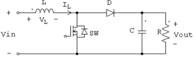
The dc-dc boost converters are used to convert the unregulated dc input to a controlled dc output at a desired voltage level. They generally perform the conversion by applying a dc voltage across an inductor or transformer for a period of time which causes current to flow through it and store energy magnetically, then switching this voltage off and causing the stored energy to be transferred to the voltage output in a controlled manner. The output voltage is regulated by adjusting the ratio of on/off time. (Kumar, Indira, Nadu, & Nadu, 2014) DC-DC converters are operated under continuous conduction mode (CCM) or discontinuous conduction mode (DCM). As the name implies, the output voltage of boost converter is higher than the input voltage. The input and output power of DC-DC converters are same for ideal case. The DC-DC boost converters operate under two cases, switch ON (SW closed) and switch OFF (SW opened) (Mohammed, 2011). Figure 2.1 shows the basic circuit of boost converter.
6
2.3 Analysis of DC-DC Boost converter
Boost converter circuit has an element that act as switch that turn ON and OFF periodically. This switching process is to ensure that the inductor that connected parallel with this switch can store and release energy when the boost converter circuit is ON or OFF mode so that the desired output voltage is achieved.
Initially, when the switch is closed, the current flow through inductor (L) and the energy is stored in inductor at this time. During the switch is opened, the stored current in the inductor then flow through load resistor (RL) and capacitor. The output voltage then produces across the load resistor (RL) and capacitor. During switch closed, the current from input supply flow through inductor and it storing energy. However, at the same time, the energy stored in the capacitor during switch opened is discharged across load resistor (Mohammed, 2011). The diode (D) is reverse biased in switch opened and it blocks the reverse flow of current from load to source (Mohammed, 2011). That why the load current and voltage is continuously produced. The voltage output is controlled by the duty cycle of the switch. Pulse is needed for controlling the switching process of the switch of DC- DC boost converter. Pulse width modulation (PWM) is general technique to generate the triggering pulse to control the switch process (Mohammed, 2011).
2.3.1 Analysis for switch Closed
This analysis is done when the switch is turn ON means that the voltages supply is flow through to inductor and the switch only. The other components that consist in the boost converter do not receive any voltage or current because of the diode become reverse biased. When the switch is closed, the diode is reversing biased (W.D. Hart, 2011). The Equation (1) of Kirchhoff’s voltage law that consist voltage source, inductor and closed switch is
7
The rate of change of current is constant, so that the current increases linearly when the switch is closed. The change in inductor current is derived as in Equation (2). ∆iL
The rate of current change when switch closed is in Equation (3).
(∆iL) close= Vs DTL (3)
Figure 2.2 refer the condition of boost converter when the switch is closed.
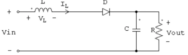
Figure 2.2: Condition of Boost converter when switch closed (Masri & Chan, 2012)
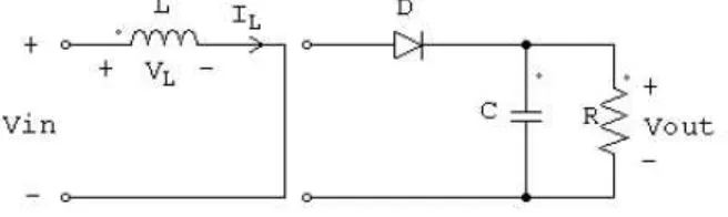
2.3.2 Analysis for switch open
8
The rate of change of inductor current is constant and current must change linearly while the switch is open. The rate of change inductor current when switch open is in Equation (7).
Figure 2.3 indicate the situation of boost converter circuit when switch is opened.
Figure 2.3: Condition of Boost converter switch is opened (Masri & Chan, 2012)
2.3.2 General analysis of boost converter condition
For steady- state operation, the net change in inductor current must be zero, by combining both equation of rate of change inductor current when closed and opened, the derive equation as Equation (8) ( W.D. Hart, 2011).
∆iL close - ∆iL open=0 (8)
Vs DT
L
+
(Vs-Vout)(1-D)T
L
=
0
(9)From the Equation (9), the output voltage can be calculated as in Equation (10)