A Novel Technique of Controlling Signal Propagation
within Array Elements using Switchable Miniaturized
Electromagnetic Band Gap
M.S.M.Isa1,2, R.J.Langley2, S.Khamas2, A.A.M.Isa1, M.S.I.M.Zin1, Z.Zakaria1, N.Z.Haron1, A.Ahmad1
Faculty of Electronic and Computer Engineering 1 Universiti Teknikal Malaysia Melaka
Melaka, Malaysia [email protected]
Department of Electronics and Electrical Engineering2 University of Sheffield
Sheffield, United Kingdom
Abstract— In this paper, a novel miniaturized capacitive loaded electromagnetic band gap (EBG) has been developed with the patch size of approximately λ/36. The dimension is controllable using the lumped capacitive elements values. The surface impedance characteristic of the EBG structure is switchable as pin vias have been inserted and removed within the EBG center and the ground plane. Switching the EBG surface impedance characteristic within the array elements has demonstrated the novel application of miniaturized EBG to control the signal propagation within the array elements. Radiation pattern for the middle antenna is enhanced toward the antenna which connected with low surface impedance EBG structure resulting approximately 12dB improvement in gain. The propagation characteristics and gain of the array have been analyzed using CST Microwave Studio (CST MWS). The new application of the EBG can be very useful to realize the controlling and channeling the signal within the array elements.
Keywords— Miniaturized EBG; Array antenna; Signal channeling; propagation; isolation; switchable; mutual coupling
I. INTRODUCTION
Mutual coupling which mainly contributed by the propagation of surface wave within array elements always be blamed for the performance degradation of the array antenna[1, 2]. Various literatures have broadly discussed the method of reducing the effect of mutual coupling including the photonic bandgap substrate [3], a defected ground plane [4, 5], and to introduce an EBG structure within the array elements [6-9]. The miniaturized and tunable EBG structure which utilized the capacitive and inductive lumped components has been illustrated in [10, 11].
In this paper, an approach to develop the miniaturized EBG structure by utilizing only capacitor lumped element has been introduced. The approach should be able to reduce the number of lumped elements required compared to [11] and reduces the tolerance errors introduced by the components.
The designed miniaturized EBG structure with unit cell period of approximately λ/36 has been achieved with the resonance frequency controllable by varying the value of the external lumped capacitors. The structure can be electronically tunable by replacing the capacitor with DC biased varactor diodes as established in [12, 13].
The inductance element for the structure has been generated by inserting the connecting pin vias into the structure. This has improved the design compactness and capability of altering the surface characteristic by switching pin vias in and out which alternately alter the surface characteristic from suppressing to conducting the surface wave[14-16].
Furthermore, the novel technique to control the mutual coupling within the array elements has been demonstrated. The technique has effectively controlled the surface wave propagation within the array elements. The simulation results using CST Microwave Studio illustrate the capability of the miniaturized EBG structure to alternately propagate and suppress the surface wave as the pin vias has been switching in and out into the structure.
The simple and various techniques for tuning the EBG operating frequency as well as the tunable surface impedance characteristics have shown the design flexibility for the proposed structure.
.
II. DEVELOPMENT OF CAPACITIVE LOADED
MINIATURIZED EBG
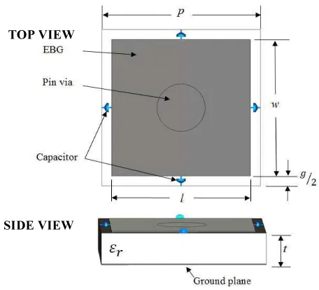
A. Unit Cell Miniaturized EBG Structure Design
The miniature EBG structure has been designed with the overall period, p and loaded with capacitors as illustrated in Fig. 1. The structure has been developed using double sided FR4 substrate with dielectric constant, Ɛr, of 4.3 and
Sponsored by : UTeM and MoHE
thickness, t of 6.4mm. The miniaturized EBG composed of PEC copper plate with switchable pin vias. The surface mount capacitors are connected within each adjacent EBG patches which act as connection current path within the cells.
Reflection phase for the EBG structure has been simulated and analyzed with various dimensions of the EBG patch and variable capacitor values. Fig. 2 shows the reflection phase of approximately 0º at 2.2GHz has been realized for 15mm mushroom-like and 3.8mm miniaturized EBG loaded with 1pF lumped capacitor. Result shows that about 75% reduction in the unit size for miniaturized EBG structure compared to mushroom-like EBG and with approximately 25% of the bandwidth for both structures has been achieved. For the case of doubling the miniaturized EBG unit cell period from 3.8mm to 7.6mm, the result shows only approximately 12% reduction in resonance frequency without significant changes in bandwidth. This is due to very small impact on the increase in sheet capacitance when increase in cell period with compared to the loaded lumped element value.
The characteristics of the EBG against the loaded capacitance value are shown in Fig. 3. In the analysis, the unit cell period, p has been fixed at 3.8mm with a 0.5mm gap within the cells. The capacitor value has been set to 0.5pF, 1pF and 2pF. The EBG unit cell reflection phase results show that the resonance frequency has decreased by more than 20% when the capacitor value is doubled. As the chosen capacitance is very large compared to the surface sheet capacitance, the bandwidth has been reduced from 0.9GHz to 0.55GHz, i.e. by approximately 40% when the capacitor value is doubled from 0.5pF to 1pF. The bandwidth is further reduced by approximately 50% when the capacitance is doubled from 1pF to 2pF. The simulated results show that the characteristics of the developed miniaturized EBG structure
are highly dependent on the loaded lumped capacitor value and marginally effected by the EBG dimensions.
B. Miniaturized EBG Design Optimisation
The optimization of the miniaturized EBG structure has been conducted using 50Ω microstrip transmission line as shown in Fig. 4. Based on the impedance calculations using CST MWS, the width of the transmission line has been determined as 12.4mm. To calculate the EBG surface transmission characteristic through the EBG structure, a couple of discrete ports have been connected at the both edges of transmission line. The EBG dimension has been tuned to achieve the best parameter of the miniaturized EBG when inserted with pin vias. The EBG band gap frequency range should covered the antenna operation frequency which has been selected as 2.2GHz. The optimized dimensions for the
Fig 1 A unit cell of miniaturized EBG with capacitors, top & side views
TOP VIEW
p= 3.8mm with 1pF capacitor p= 7.6mm with 1pF capacitor p=15mm without capacitor
Fig. 2: Simulated reflection phase for a unit cell EBG
frequency (GHz)
Fig. 4: Miniaturized EBG structure with microstrip transmission line
miniaturized EBG structure have been determined as:
p=3.8mm; l=w=3.3mm; g=0.5mm and CL=0.5pF. The value of the capacitor has been calculated as halve of the value for the capacitance simulated in EBG unit cell due to two 1pF capacitors which come from each cell have been connected in series within the cells. The structure has been simulated using an FR4 material substrate with a dielectric constant of Ɛr =4.3 and a thickness of 6.4mm.
The transmission loss across the optimized dimension of the miniaturized EBG surface for the case of EBG with and without pin vias has been compiled as presented in Fig. 5. Result dictates that the switching pin vias in and out has alternately switched the EBG characteristic from suppressing to propagating the surface wave, which denoted by the reduction and increment in EBG surface transmission values respectively. The EBG structure will be used in the next section to analyze the characteristic of EBG to control the propagation of signal or surface wave within the array elements.
III. SIGNAL PROPAGATION CONTROL WITHIN THE ARRAY
ELEMENTS USING MINIATURIZED EBG.
In this section, the analysis and applications of the miniaturized EBG structure to control the propagation and
suppression of surface wave within the array elements are demonstrated. Three identical microstrip patch antennas with the width and length of 28.6 mm have been arranged in series as shown in Fig. 6. The patch antennas have been denoted as Antenna1, Antenna2, and Antenna3 and separated by a distance of 82mm (0.6λ2.2GHz).
The miniaturized EBG structure with a period of 3.8mm and connected with a 0.5pF lumped capacitor has been placed within the array elements. Pin vias have been placed at the middle of each EBG patches which is similar to the miniaturized EBG structure designed in the previous section. The EBG structure has been denoted as EBG-A and EBG-B as shown in Fig. 6. Array antennas and miniaturized EBG structure have been constructed on an FR4 PCB with a thickness and a relative dielectric constant of 6.4mm and 4.3, respectively.
To investigate the effectiveness of the miniaturized EBG to control the flow of surface wave within the array elements, pin vias at each sector, EBG-A and EBG-B, have been switched out and in respectively. This is expected should be able to alternately alter the EBG sector impedance characteristics accordingly.
Fig. 6: Microstrip patch array antenna integrated with miniaturized EBG structure. Discrete port
Transmission microstrip line
EBG
Pin via Capacitor
Frequency / GHz
1.4 1.5 1.6 1.7 1.8 1.9 2.0 2.1 2.2 2.3 2.4 2.5 2.6 2.7 2.8 2.9 3.0
T
ra
n
s
m
is
s
io
n
/
d
B
-50 -40 -30 -20 -10 0
S12 EBG without via S12 EBG with via
Fig. 5: Surface transmission los for miniaturized EBG structure
x EBG-A
(No pin via)
EBG-B (with pin via)
Antenna2
Port 1
Port 2 Port 3
Ground plane Antenna1 Antenna3
y
z x
Simulated mutual coupling results for the case of the pin vias have been switched out from the EBG-A, and switched in for the EBG-B is demonstrated in Fig. 7. The results show a reduction of approximately 9dB in the mutual coupling between Antenna1 and Antenna3, S31 at the operating frequency of 2.2GHz has been observed. This is mainly due to the existence of the miniaturized EBG structure inserted with pin vias within the array element which exhibits the band gap properties. This has efficiently suppressed the surface waves within the elements which represented by the reduction in mutual coupling.
For the case of removing or switch out the pin vias from sector EBG-B, the EBG’s high impedance properties at the antenna operating frequency has been eliminated, which in return has altered the EBG’s surface from band gap with high impedance surface to low impedance surface. The enhancement of mutual coupling between Antenna1 and Antenna2, S21 illustrates the improvement of surface wave propagation within the array elements. These results demonstrate the effectiveness of the miniaturized EBG to control the propagation and suppression of surface wave.
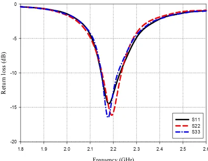
Return loss results for all the array elements when the EBG structure has been altered are shown in Fig. 8. The frequency of the minimum return loss for Antenna1, S11and Antenna3,
S33are slightly less than Antenna2, S22. This different is due to
the slight changed in the total antenna cavity as the pin vias are inserted and removed. However, the results demonstrate that the entire antennas are remained stable at the desired operating frequency of 2.2GHz.
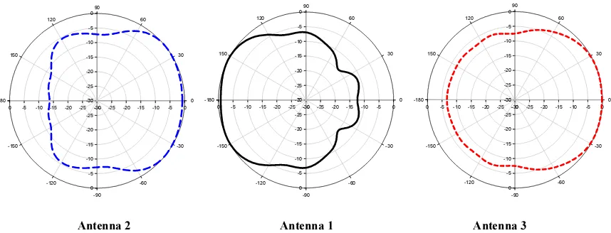
Normalized azimuth radiation patterns for the array element are plotted in Fig. 9. Radiation patterns illustrate the performance of the miniaturized EBG to control the propagation of the surface radiation power between the array elements against Antenna1 at the middle. The high mutual coupling between Antenna1 and Antenna2, S21 represents the enhancement of surface wave propagation within the array elements. This is demonstrated by the radiation pattern for
Antenna2 directing towards Antenna1 with approximately 13dB enhancement in the gain.
However, radiation pattern for Antenna3 is almost circular in shape with approximately 7dB reduction in gain away from Antenna1. The pattern’s shape is caused by the isolation between these antennas as the result of the surface wave suppression, and also due to the reflection of the radiation power away from the EBG surface.
Radiation pattern for the middle element of Antenna1, is directed towards Antenna2 and reflected from Antenna3 with approximately 12dB reduction in gain at the direction facing toward Antenna3. The result illustrates the agreement of the result for the surface wave propagation and suppression within the array elements which have been demonstrated by the radiation patterns of antennas 2 and 3.
Therefore, switching pin vias in and out has alternately altered the structure’s surface impedance, which can be utilized to control the surface wave’s propagation within the array elements. The miniaturized EBG structure inserted with pin vias illustrates the high surface impedance feature, which suppresses the surface wave’s propagation and having the unique characteristic of reflecting the radiation away from its surface. Whereas, the miniaturized EBG structure without pin vias illustrates the low impedance characteristic, which allows the propagation of surface wave. The novel finding is important for the EBG to be utilized in controlling the propagation and suppressing the signal within array elements.
IV. CONCLUSION
In this paper, a novel compact miniaturized capacitive loaded EBG with a period of 3.8mm (λ0/36) has been
developed. The application of miniaturized EBG to control the surface wave propagation within the array element has been established by switching the pin vias in and out at each EBG sections. Switching in pin vias into the EBG patches establish the structure with band gap characteristic. Placing the EBG
Fig. 8: Return loss for the array elements
Frequency (GHz)
structure within the array elements has suppressed the surface waves and improved the isolation within the array elements. Removing the pin vias from the miniaturized EBG patches has altered the structure to the low surface impedance. Placing the structure within the array elements has demonstrated the new novel application of EBG in propagating the signal within the array elements.
The novel finding on the new application of the EBG to control the signal propagation within the array elements has been achieved. Switching pin vias in and out could establish the smart controlling of signal propagation through the EBG surface with approximately 12dB enhancement in gain for the middle antenna. The structure can be utilized for channeling the signal within the elements in wireless system and local wireless network such as for body area network (BAN).
ACKNOWLEDGMENT
The authors would like to thank University of Sheffield for their facilities. Great gratitude to Universiti Teknikal Malaysia Melaka (UTeM) and Ministry of Higher Education for their “Research Acculturation Grant: RAGS/2012/FKEKK/TK02/2 B0005“.
REFERENCES
[1] D. Pozar and D. Schaubert, "Scan blindness in infinite phased arrays of
printed dipoles," IEEE Transactions on Antennas and Propagation, vol. 32, pp. 602-610, 1984.
[2] M. A. Khayat, J. T. Williams, D. R. Jackson, and S. A. Long, "Mutual
coupling between reduced surface-wave microstrip antennas," IEEE Transactions on Antennas and Propagation, vol. 48, pp. 1581-1593, 2000.
[3] R. Gonzalo, P. De Maagt, and M. Sorolla, "Enhanced patch-antenna
performance by suppressing surface waves using photonic-bandgap substrates," IEEE Transactions on Microwave Theory and Techniques, vol. 47, pp. 2131-2138, 1999.
[4] S. Xiao, M. C. Tang, Y. Y. Bai, S. Gao, and B. Z. Wang, "Mutual
coupling suppression in microstrip array using defected ground structure," IET Microwaves, Antennas & Propagation, vol. 5, pp. 1488-1494, 2011.
[5] M. K. Mandal and S. Sanyal, "A Novel Defected Ground Structure for
Planar Circuits," IEEE Microwave and Wireless Components Letters, vol. 16, pp. 93-95, 2006.
[6] D. Sievenpiper, Z. Lijun, R. F. J. Broas, N. G. A. A. N. G. Alexopolous,
and E. A. Y. E. Yablonovitch, "High-impedance electromagnetic surfaces with a forbidden frequency band," IEEE Transactions on Microwave Theory and Techniques, vol. 47, pp. 2059-2074, 1999.
[7] Y. Ang and Z. Xuexia, "A Novel 2-D Electromagnetic Band-Gap
Structure and its Application in Micro-strip Antenna Arrays," 3rd International Conference on Microwave and Millimeter Wave Technology Proceedings, pp. 580-583, 2002.
[8] Y. Fan and Y. Rahmat-Samii, "Microstrip antennas integrated with
electromagnetic band-gap (EBG) structures: a low mutual coupling design for array applications," IEEE Transactions on Antennas and Propagation, vol. 51, pp. 2936-2946, 2003.
[9] M. F. Abedin and M. Ali, "Reducing the Mutual-Coupling between the
Elements of a Printed Dipole Array using Planar EBG Structures," IEEE Antennas and Propagation Society International Symposium, vol. 2A, pp. 598-601, 2005.
[10] H. Liu, K. L. Ford, and R. J. Langley, "Novel Planar Band Pass
Lump-Loaded Frequency Selective Surface," IEEE MTT-S International Microwave Workshop Series on Art of Miniaturizing RF and Microwave Passive Components, pp. 87-89, 2008.
[11] L. Hui Lai, K. L. Ford, and R. J. Langley, "Design Methodology for a
Miniaturized Frequency Selective Surface Using Lumped Reactive Components," IEEE Transactions on Antennas and Propagation, vol. 57, pp. 2732-2738, 2009.
[12] B. Sanz-Izquierdo, E. A. Parker, J. B. Robertson, and J. C. Batchelor,
"Tuning technique for active FSS arrays," Electronics Letters, vol. 45, pp. 1107-1109, 2009.
[13] C. Mias, "Varactor-tunable frequency selective surface with
resistive-lumped-element biasing grids," IEEE Microwave and Wireless Components Letters, vol. 15, pp. 570-572, 2005.
[14] M. S. Mohamad Isa, R. J. Langley, S. Khamas, A. Awang Md Isa, M. S.
I. M. Zin, F. M. Johar, and Z. Zakaria, "Antenna Beam Steering using Sectorized Square EBG," Journal of Telecommunication, Electronic and Computer Engineering (JTEC), vol. 4 No 1, pp. 39-44, 2012.
[15] M. S. Mohamad Isa, R. J. Langley, and S. Khamas, "Antenna control
using EBG," Proceedings of the 5th European Conference on Antennas and Propagation (EUCAP), pp. 216-219, 2011.
[16] M. S. Mohamad Isa, R. J. Langley, and S. Khamas, "Antenna pattern
diversity using EBG," Loughborough Antennas and Propagation Conference (LAPC), 2010, pp. 325-328, 2010..
-30 -25 -20 -15 -10 -5 0