DESIGN AND DEVELOPMENT OF AN RF POWER HARVESTER OPERATING IN SUBTHRESHOLD FOR BODY AREA NETWORKS
TAN PEI CHEE
This Report Is Submitted in Partial Fulfilment of Requirements for The Bachelor Degree of Electronic Engineering (Telecommunication Electronics)
Faculty of Electronics and Computer Engineering
Universiti Teknikal Malaysia Melaka
v
ACKNOWLEDGEMENT
At the end of my thesis, I would like to thank all those people who made this thesis possible and an unforgettable experience for me. This final year project report could not be realized without the sincere help and support from many people. I am very appreciating their help and support.
Firstly, I would like to express my deepest sense of gratitude to my supervisor, Dr. Wong Yan Chiew who offered her continuous advice and encouragement throughout this project. She is a nice lecturer who always giving her students enough space to perform and develop. I thank her for the excellent guidance and great effort she put into training me in the analog IC design field.
Next, I thankful to my friends especially BENT colleagues who give the motivation and encouragement along the way to make this thesis successful. Special thanks to my friends, Lee YouHui and Ang Wei Pin for their helping, sharing of knowledge and guidance throughout the project. I am much appreciated with the friendships as well as good advice and collaboration has been built up.
vi
ABSTRACT
vii
ABSTRAK
viii
TABLE OF CONTENTS
CHAPTER CONTENT PAGE NUMBER
PROJECT TITLE
CONFIRMATION ON REPORT STATUS DECLARATION
SUPERVISOR’S CONFIRMATION ACKNOWLEDGEMENT
ABSTRACT ABSTRAK
TABLE OF CONTENTS LIST OF TABLES
LIST OF FIGURES
LIST OF ABBREVIATIONS
I INTRODUCTION
1.1 Project Overview 1
1.2 Problem Statement 2
1.3 Objectives 2
1.4 Scope of Work 2
1.5 Project Development 3
1.6 Report Outline 3
ix
II LITERATURE REVIEW
2.1 Overview 5
2.2 Body Area Network (BAN) 5 2.3 RF Energy Harvesting System 6
2.4 Rectifier 6
2.5 Operating Region of MOSFET 8
2.5.1 Subthreshold Region 9
2.5.2 Linear Region 9
2.5.3 Saturation Region 9
2.6 Design Consideration of High Quality Rectifier 9 2.6.1 High Power Conversion Efficiency/High
Output Voltage 9
2.6.2 Small Circuit Size 10
2.6.3 High Sensitivity 10
2.6.4 Low Threshold Voltage 11
2.6.5 Size of Transistor 11
2.6.6 Low Leakage Current 12
2.6.7 Faster Rise Time 12
2.6.8 Low Ripple or Noise 12 2.7 RF Rectifier Topologies Based on MOSFET 12 2.7.1 Fully Gate Cross Coupler (FGCC) rectifier 13 2.7.2 Self Vth Cancellation (SVC) Rectifier 14 2.7.3 Dynamic Threshold-voltage MOSFET
(DTMOS) Rectifier 14
2.7.4 Comparison among Topologies 15 2.8 Charge Transfer Switches in Integrated Circuit
(IC) Domain 16
2.8.1 Schottky Diode 17
2.8.2 Diode-Connected PMOS Diode 17 2.8.3 Ultra-Low Power (ULP) Diode 17
2.9 Summary 18
x
III METHODOLOGY
3.1 Overview 19
3.2 Specifications Setting 20
3.3 Schematic Design 20
3.4 Layout Design 20
3.5 Summary 20
IV COMPARISON ON THE TOPOLOGIES OF RECTIFIER
4.1 Overview 22
4.2 Circuit Construction According to Rectifier
Topologies 22
4.3 Parameters Setting at Different Topologies
and Technologies 23
4.4 Simulation Result and Analysis According
to Rectifier Topologies 27
4.5 Summary 28
V COMPARISON ON CHARGE TRANSFER SWITCHES
5.1 Overview 29
5.2 Schematic Design of Diode-Connected PMOS and ULP Diode Applied in Villard Voltage
Multiplier and Dickson Charge Pump Rectifier 31 5.2.1 Leakage Current Analysis 33 5.2.2 Transient Analysis on Output Voltage 36 5.3 Parameter Optimization in Dickson Charge
Pump Rectifier using ULP diode 37
xi
5.5 Layout Design 41
5.6 Summary 44
VI MODELLING AND PROTOTYPING OF A SIMPLE ENERGY HARVESTING
6.1 Overview 45
6.2 Antenna 45
6.3 Impedance Matching 46
6.4 Prototype of Dickson Charge Pump
Converter using Diode IN5819 47
6.5 Summary 51
V CONCLUSION
7.1 Overview 52
7.2 Project Summary 52
7.3 Future Work Suggestion 54
REFERENCES 55
APPENDIX 57
Appendix A: A Review & Analysis on High Sensitivity
RF Rectifier in BAN devices 57
Appendix B: Dickson Charge Pump Rectifier using
xii
LIST OF TABLES
No. TITLE PAGE
2.1 Operating region in NMOS and PMOS transistor 8 2.2 Performances summary for different topologies 16
3.1 Specifications setting 20
4.1 Parameter setting for rectifier topologies in different
technologies 24
5.1 Parameter setting in Villard voltage multiplier and Dickson
xiii
LIST OF FIGURES
No. TITLE PAGE
2.1 Block diagram of RF harvesting system 6
2.2 Half-wave Rectification 7
2 3 Full-wave Rectification 7
2.4 Circuit configuration and circuit operation of FGCC rectifier 13 2.5 Circuit configuration of SVC rectifier 14 2.6 Circuit configuration of DTMOS rectifier 15
2.7 Diode-connected PMOS diode 17
2.8 Ultra-Low Power (ULP) diode 18
3.1 Methodology for the project 19
4.1 3 stages FGCC rectifier schematic design 23 4.2 3 stages SVC rectifier schematic design 23 4.3 3 stages DTMOS rectifier schematic design 23 4.4 Transient analysis on output voltage of FGCC in 90nm
technology with different width of transistor 25 4.5 Transient analysis on output voltage of SVC rectifier in 90nm
technology with different width of transistors 25 4.6 Transient analysis on output voltage of DTMOS in 90nm
technology with different width of transistors 25 4.7 Transient analysis on output voltage of FGCC in 130nm
technology with different width of transistors 26
4.8 Transient analysis on output voltage of SVC in 130nm
xiv
4.9 Transient analysis on output voltage of DTMOS in 130nm
technology with different width of transistor 26 4.10 Transient analysis on output voltage of different topologies
in 90nm and 130nm technology 27
4.11 Output voltage versus input voltage for different topologies
and technologies 28
5.1 Voltage doubler circuit 30
5.2 Villard voltage multiplier 30
5.3 Dickson charge pump rectifier 30
5.4 3 Stages Villard Voltage Multiplier Using Diode-Connected PMOS 31 5.5 3 Stages Villard Voltage Multiplier Using ULP diodes 32 5.6 3 Stages Dickson Charge Pump Using Diode-Connected PMOS 32 5.7 3 Stages Dickson Charge Pump Using ULP Diodes 32 5.8 Leakage current of each diode-connected MOSFET in Villard
voltage multiplier 34
5.9 Leakage current of each ULP diode in Villard voltage multiplier 34 5.10 Leakage current of each diode-connected MOSFET in Dickson
Charge Pump rectifier 34
5.11 Leakage current of each ULP diode in Dickson Charge Pump rectifier 35 5.12 Leakage Current of PMOS in diode-connected MOSFET and
ULP in Dickson Charge Pump rectifier 35
5.13 Node Voltage of PMOS in ULP and diode-connected MOSFET
in Dickson Charge Pump rectifier 36
5.14 Transient Analysis of Output Voltage using ULP diode and diode-connected MOSFET in Villard Voltage Multiplier and
Dickson Charge Pump rectifier 36
5.15 Power Efficiency versus Frequency 37
xv
5.19 Power Efficiency versus Load Capacitance 39 5.20 Power Efficiency versus Load Resistance 40 5.21 Power Efficiency versus Load Resistance in 650MHz 40 5.22 Transient Analysis on Output Voltage of Dickson Charge
Pump Using ULP Diodes 41
5.23 Output Voltage versus Input Voltage in Dickson Charge Pump
using ULP Diodes 41
5.24 Layout of 3 stages Dickson charge pump rectifier 42 5.25 Interdigitation pattern of NMOS in ABBA 43 5.26 Dummy which mentioned end-to-end connection applied in NMOS 43 5.27 Matching single transistor in layout 43
6.1 Simple RF energy harvesting system 45
6.2 Basic structure of dual band planar monopole antenna. The dashed square shows the ground plane on the back of the PCB.
Metal strip lines M1, M2, and M3 are on the top of the PCB 46
6.3 Antenna parameter setting 46
6.4 Reflection coefficient S11 at 900MHz is < -20dB 46 6.5 Measured input impedance of 8 stages Dickson charge pump
rectifier using diode IN5819 47
6.6 Matching network in microstrip line design 47 6.7 Graph of return loss for microstrip line matching network 47 6.8 Schematic design of 8 stages Dickson Charge pump using IN5819 48 6.9 Simulation result on transient analysis of rectified output voltages
for different input voltages 48
6.10 PCB layout of 8 stages Dickson charge pump 49 6.11 Fabricated 8 stages Dickson charge pump rectifier using
diode IN5819 49
6.12 Measurement setup for Dickson charger pump converter prototype 49 6.13 Measured output voltage versus Vrms in the frequencies setting
xvi
6.14 Output power for different source frequencies for
xvii
LIST OF ABBREVIATIONS
EEG - Electroencephalography
BAN - Body Area Network
RF - Radio Frequency
DC - Direct Current
PCE - Power Conversion Efficiency
CMOS - Complementary Metal Oxide Semiconductor DRC - Design Rule Checking
LVS - Layout Versus Schematic
MOSFET - Metal Oxide Semiconductor Field Effect Transistor FGCC - Fully Gate Cross Coupler
SVC - Self Vth Cancellation
DTMOS - Dynamic Threshold-voltage MOSFET
IC - Integrated Circuit
ULP - Ultra Low Power
PCB - Printed Circuit Board
LIP - Low Input Power
BCU - Body Central Unit
BSU - Body Sensor Unit
AC - Alternate Current
NMOS - N-type MOSFET
1
CHAPTER 1
INTRODUCTION
1
1.1 Project Overview
2
1.2 Problem Statement
RF energy is a widely available energy source due to continuous broadcasting from radio sources like mobile phones, television broadcast stations, and others. However, the ambient RF power signal is usually too weak [2] and it is not able to turn on the traditional rectifiers to operate. It is usually lower than the threshold voltage of the transistor. But it should not being wasted and can be used to power up the low power consumption BAN devices. Besides, the threshold voltage of the transistors also affects the performance of PCE. More stages used will also degrade the PCE. Not only that, the high power consumption and small battery size also severely limit the operating time of sensor devices in BAN [1]. Therefore, there is a need for high sensitivity RF rectifier design. The RF rectifier should have the ability for harvesting efficiently energy from RF sources to enable the wireless charging of low power devices in BAN. Thus, the cost for purchasing the battery can be saved since the battery replacement can be eliminated through wireless charging devices.
1.3 Objectives
The main objectives of this project are:
- To investigate the topologies of RF rectifier
- To design RF rectifier with high sensitivity
- To enhance the PCE of RF rectifier
- To develop the proposed design into a layout
1.4 Score of Project
3
1.5 Project Development
The RF rectifier design involves a few stages where the first stage is to study and understand the operation of existing topologies and compare its simulated result by using Synopsys simulator. The second stage is to set the specifications. Then, the circuit will be designed in schematic and simulated to verify whether the design match with the specifications mentioned. If the design meets the specifications set, then proceed to the layout design, Design Rule Checking (DRC) checking, Layout Versus Schematic (LVS) checking and parasitic extraction. Next, the last verification will do to ensure the design is match with the specifications set. Lastly, the RF rectifier design was completed once the last verification meets the specifications set.
1.6 Report Outline
This thesis consists of five chapters. It explains and discusses each description and detail for each chapter.
Chapter I – Introduction
The important parts of the project have been introduced. Section 1.5 presents the project development. The scope of the project is focused on the RF rectifier.
Chapter II - Literature Review
The important terms such as BAN, RF harvesting system, rectifier, operating region of Metal Oxide Semiconductor Field Effect Transistor (MOSFET) transistor and design consideration of high-quality rectifier have been described. Section 2.7 presents the RF rectifier topologies based on MOSFET which are Fully Gate Cross Coupler (FGCC) rectifier, Self Vth Cancellation (SVC) rectifier and Dynamic Threshold-voltage MOSFET (DTMOS) rectifier. Their specifications, advantages, disadvantages, circuit design and operation have been reviewed. Charge transfer switches in Integrated Circuit (IC) domain have been studied in Section 2.8. It includes Schottky diode, diode-connected diode and Ultra-Low Power (ULP) diode.
Chapter III – Methodology
4
simulated in order to achieve the specification set. Lastly, the layout design included DRC checking, LVS checking, and parasitic extraction were discussed in Section 3.4.
Chapter IV – Comparison on RF Rectifier Based on MOSFET
The overview of this chapter has been presented in Section 4.1. Section 4.3 shows the schematic design of FGCC, SVC, and DTMOS rectifier while Section 4.3 shows the parameter setting at 90nm and 130nm technology for RF rectifier topologies. The optimization on the width of transistors has been carried out. The simulation result and analysis in term of rise time and the output voltage of RF rectifiers have been reviewed in Section 4.4.
Chapter V – Comparison on Charge Transfer Switches in IC Domain
The voltage multiplier rectifier topologies include Villard voltage multiplier and Dickson charge pump rectifier have been reviewed in Section 5.2. Section 5.3 shows the schematic design of Villard voltage multiplier and Dickson charge pump rectifier applied with the charge transfer switches. Their simulation result in term of leakage current and output voltage have been presented in Section 5.3.1 and 5.3.2 respectively. Section 5.4 presents the parameters optimization in the Dickson charge pump using ULP diode. The high sensitivity rectifier shows in Section 5.5 and proceeds to a layout designed in Section 5.6.
Chapter VI – Modeling and Prototyping of A Simple RF Harvesting System A block diagram of RF energy harvesting has been reviewed in Section 6.1. Section 6.2 shows a dual-band planar antenna design which operates in 900MHz and 1900MHz. Then, microstrip single stub matching network has been investigated in Section 6.3. Lastly, 8 stages of Dickson Charge Pump using diode IN5819 has been simulated and then fabricated in a Printed Circuit Board (PCB) as shown in Section 6.4. The simulated and measured results obtained have been analyzed and discussed.
Chapter VII – Conclusion and Recommendation
A high sensitivity RF rectifier design which applied in BAN is presented. The result and analysis for the whole project were concluded in Section 7.1. The future works have been discussed and suggested in Section 7.2.
5
CHAPTER 2
LITERATURE REVIEW
2 O
2.1 Overview
In this chapter, it includes the reviews on BAN, RF harvesting system, rectifier, operating region of MOSFET transistor, characteristics of the high-quality rectifier. Besides, the topologies such as Fully Gate Cross Coupler (FGCC) rectifier, Self Vth Cancellation (SVC) rectifier and Dynamic Threshold-voltage MOSFET (DTMOS) rectifier have been reviewed. The charge transfer switches in IC domain such as Schottky diode, diode-connected MOSFET, and ULP diode have been studied.
2.2 Body Area Network (BAN)
6
2.3 RF Energy Harvesting
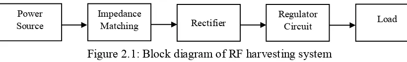
RF energy harvest is one of the popular types of power harvesting. The goal of an RF energy harvester is to convert the ambient RF energy sources into a stable DC power. A block diagram of RF harvesting system shown in Figure 2.1 [4]. It consists of the power source, impedance matching, rectifier, regulator circuit, and load. The power source is generally an antenna were used to capture the ambient RF signal while the impedance matching circuit is required to ensure the maximum RF energy is transferred from the source to load. In another word, it is used to match the impedance of antenna and rectifier in order to reduce the loss in the system. Next, the rectifier circuits convert the received RF signal voltage into a stable output DC voltage. When the output voltage of rectifier is not stable, a regulator circuit is a function to provide a smooth, stable and ripple free DC voltage. Lastly, the load is where the produced power is delivered to related applications or devices.
The rapid expansion of sensor network requires a reliable power supply to replace the battery. However, the battery technology still in the slow progress to catch up with the latest electronic devices especially in nanometer (nm) technology where existing batteries are not fixed for such miniaturization[4]. With the RF harvesting system, the battery could be replaced by RF power harvesting devices to provide an independent energy source. Therefore, the need of battery could be eliminated and it is able to save on the operation and maintenance cost. Thus, this alternative source of energy has brought lots of attention for development.
2.4 Rectifier
A rectifier is also known as RF to DC converter which necessary to provide a stable power supply with the required voltage level [5]. The rectification occurs in both half-wave and full wave rectifier as shown in Figure 2.2 and Figure 2.3. The half-wave rectification allows either the positive or negative half of the alternating current (AC) signal to pass through and block the other half. While the full-wave rectification
Power
[image:23.595.115.525.365.428.2]Source Impedance Matching Rectifier Regulator Circuit Load
7
converts both polarities of the alternate current (AC) input waveform to pulsating DC. Thus, a higher average output voltage is able to produce. However, more ripple will be produced in half-wave rectifier compared to full-wave rectifiers. Therefore, much more filtering is needed to eliminate harmonics of the AC frequency from the output in half-wave rectification process.
Figure 2.2 : Half-wave rectification
Figure 2.3 : Full-wave rectification