i
DESIGN AND FABRICATION OF SUBSTRATE INTEGRATED WAVEGUIDE BANDSTOP FILTER
SITI SABARIAH BT SABRI
This Report Is Submitted In Partial Fulfillment of Requirements For The Bachelor Degree of Electronic Engineering (Wireless Communication)
Faculty of Electronic and Computer Engineering Universiti Teknikal Malaysia Melaka
ii
UNIVERSTI TEKNIKAL MALAYSIA MELAKA
FAKULTI KEJURUTERAAN ELEKTRONIK DAN KEJURUTERAAN KOMPUTER BORANG PENGESAHAN STATUS LAPORAN
PROJEK SARJANA MUDA II
Tajuk Projek : Design and Fabrication of SIW Bandstop Fliter
Sesi
Pengajian :
1 0 / 1 1
Saya Siti Sabariah Bt Sabri
mengaku membenarkan Laporan Projek Sarjana Muda ini disimpan di Perpustakaan dengan syarat-syarat kegunaan seperti berikut:
1. Laporan adalah hakmilik Universiti Teknikal Malaysia Melaka.
2. Perpustakaan dibenarkan membuat salinan untuk tujuan pengajian sahaja.
3. Perpustakaan dibenarkan membuat salinan laporan ini sebagai bahan pertukaran antara institusi pengajian tinggi.
4. Sila tandakan ( √ ) :
SULIT*
*(Mengandungi maklumat yang berdarjah keselamatan atau kepentingan Malaysia seperti yang termaktub di dalam AKTA RAHSIA RASMI 1972)
TERHAD** **(Mengandungi maklumat terhad yang telah ditentukan oleh organisasi/badan di mana penyelidikan dijalankan)
TIDAK TERHAD
Disahkan oleh:
__________________________ ___________________________________
(TANDATANGAN PENULIS) (COP DAN TANDATANGAN PENYELIA)
iii
“ I hereby declared that this report entitled Design and Fabrication of SIW Bandstop Filter is a result of my own work except for quoted that have been cited clearly in the
references”
Signature : ……….
Student : SITI SABARIAH BT SABRI
iv
“I hereby declared that I have read this report and in my opinion this report is sufficient in term of the scope and quality for the award the Bachelor of Electronic Engineering
(Wireless Communication) With Honours”
Signature : ……….
Supervisor Name : DR.BADRUL HISHAM BIN AHMAD
v
Specially dedicate to my beloved parent, Sabri Bin Mat Ali and Siti Khodijah Bt
Hashim and also to my siblings who give the encouragement and support for me to
completed this thesis. Not forgotten to my supervisor Dr.Badrul Hisham Bin Ahmad
who gave me lot of guidance and advice throughout this project until successful. Thanks
vi
ABSTRACT
This paper presents the designs of Substrate Integrated Waveguide (SIW)
bandstop filter. In order to give the bandstop response, this network comprises a
Substrate Integrated Waveguide (SIW) cavity resonator which is coupled to a strip line.
SIW are high performance broadband interconnects with excellent immunity to
electromagnetic interference and suitable for use in microwave and millimeter-wave
electronics, as well as wideband systems. They are very low-cost in comparison to the
classic milled metallic waveguides as they may be developed using inexpensive printed
circuit board (PCB) fabrication techniques. With the advent of SIW technology in
microwave area, many circuits are designed based on these structures. SIW is
synthesized by placing two rows of metallic via-holes in a substrate. The field
distribution in an SIW is similar to that in a conventional rectangular waveguide.
Hence, it takes the advantages of low cost, high Q-factor and can easily be integrated
into microwave and millimeter wave integrated circuits. The transmission loss of the on
substrate transitions may be much lower than that of the transitions or coupling sections
made between the conventional waveguide and planar circuits. Whilst many researches
using this technology are being carried out, this project proposes that instead of
designing bandstop filter based on a SIW rectangular or square resonator. In order to
develop a bandstop filter base on the SIW rectangular resonator, cavity resonator
coupled to a strip line to give bandstop response. The microstrip probe was positioned
in the middle of SIW resonator to ensure only the TE10 mode was excited. The size of
the resonators, diameters of the metal posts and spacing of adjacent posts are consider
based from with the length of the resonators approximate to a half guide wavelength
vii
ABSTRAK
Projek ini menerangkan mengenai reka bentuk Substrate Integrated Waveguide
(SIW) bandstop filter. Untuk memberikan respon bandstop, rangkaian ini terdiri
daripada Substrate Integrated Waveguide (SIW) resonator rongga yang digabungkan
dengan garis jalur . Mereka sangat murah berbanding dengan pandu klasik logam giling
kerana mungkin akan dibangunkan dengan menggunakan papan litar murah bercetak
(PCB) teknik fabrikasi. Dengan munculnya teknologi gelombang mikro SIW, banyak
litar direka berdasarkan struktur ini. SIW disintesis dengan meletakkan dua baris logam
melalui-lubang di substrat. Edaran lapangan di sebuah SIW adalah serupa dengan yang
di pandu gelombang persegi panjang konvensional. Oleh kerana itu, mengambil
keuntungan dari kos rendah, tinggi Q-faktor dan dengan mudah dapat diintegrasikan ke
dalam rangkaian gelombang mikro dan milimeter bersepadu. Hilangnya penularan pada
peralihan substrat mungkin jauh lebih rendah berbanding dengan peralihan atau
bahagian gandingan dibuat antara pandu gelombang konvensional dan litar
planar. Sementara banyak kajian menggunakan teknologi ini sedang dilaksanakan,
projek ini mencadangkan bahawa merancang penapis bandstop berdasarkan resonator
SIW persegi panjang atau bujur sangkar. Dalam rangka mengembangkan asas penapis
bandstop pada resonator SIW persegi panjang, resonator rongga digabungkan ke saluran
jalur untuk untuk memberikan respon bandstop. Jalur mikro probe diposisikan di tengah
resonator SIW untuk memastikan hanya mod TE10 sangat senang. Saiz resonator,
diameter posting logam dan jarak yang berdekatan posting mempertimbangkan
berdasarkan dari dengan panjang resonator anggaran dengan panjang gelombang
viii
ACKNOWLEDGEMENTS
To begin, I must say special thanks to my parents Sabri bin Mat Ali and Siti
Khodijah Bt Hashim for their support, encouragement and most importantly their
prayers for me to going through my study in UTeM.
I would like to thank to my supervisor, Dr. Badrul Hisham Ahmad, for your
guidance and support during my studies on my project.
ix
TABLE OF CONTENTS
CHAPTER TITLE
ABSTRACT
ACKNOWLEDGEMENT TABLE OF CONTENTS LIST OF TABLE
LIST OF FIGURES LIST OF SYMBOLS
PAGE vi viii ix xii xiii xv 1.0 2.0 INTRODUCTION
1.1 Project Background
1.2 Problems Statement
1.3 Project Objectives
1.4 Scopes
1.5 Methodology
1.6 Report Structure
LITERATURE REVIEW
2.1 Introduction
2.2 RF and Microwave Filter
2.3 Introduction of SIW
x
3.0
4.0
2.4 Implementation of SIW
2.5 SIW Transitions
2.6 Transition Between Planar Circuit and SIW
2.7 SIW Filters and Cavity Resonators
2.8 Various Transmission Lines
2.81 Coplanar Waveguide (CPW)
2.8.2 Microsrtip Line
2.8.3 Rectangular Waveguide
2.9 Via Hiles
2.10 Operation Frequency
2.11 Connectors
METHODOLOGY
3.1 Introduction
3.2 Flow Chart
3.3 Process Outline
3.4 Design Process
3.5 Manufacturing Process
3.5.1 Etching Process
3.5.2 Drilling and Soldering The Board
RESULT AND DISCUSSION
4.1 Introduction
4.2 Results
4.2.1 Simulation
4.2.2 Measurement
4.3 Results Analysis
xi
5.0 CONCLUSION
4.4 Conclusion
4.5 Recommendation
REFERENCES
APPENDIX
53
54
55
xii
LIST OF TABLES
TABLE TITLE PAGE
1
2
Standard waveguides
Variation of Microstrip Width with Q Factor
25
xiii
LIST OF FIGURES
FIGURE TITLE PAGE
1.1 Flow Chart for the whole process of the project 5
2.1 RF Front End of a Cellular Base Station 8
2.2 Model of SIW 12
2.3 TE10 Surface Current Distribution on RWG 13
2.4 Various Transmission Line 18
2.5 Microstrip Line 21
2.6 The Field Distribution of a Microstrip 21
2.7 Geometry of a Rectangular Waveguide 23
2.8 Electrical and Magnetic Fields for the TE10 Mode in a
Rectangular Waveguide
24
2.9 Cross Section of a Plated Through Hole or Via 27
2.10 Typical Hole Pattern Under BGA 28
3.1 Flow Chart for the Whole Process of the Project 32
3.2 Rectangular Waveguide 27
3.3 Diameter and Pitch for Via Hole 38
3.4 Via Hole in ADS 39
3.5 Microstrip Line 39
3.6 Filter Design in ADS 40
3.7 After Inserted The Via Hole 42
3.8 UV Machine 43
xiv
3.10 Drilling Process 45
3.11 Soldering Process 46
3.12 SMA Connector 46
4.1 Filter Design in ADS Momentum 48
4.2 A Simulated Frequencies Response for a Single Stage SIW
Bandstop Filter with Arrays of Via Holes
49
4.3 Prototype of SIW Bandstop Filter 49
4.4 Side View of SIW Bandstop Filter 50
xv
LIST OF SYMBOLS
λg Guide wavelength
λo Center frequency wavelength
fo Center frequency
ωc Cut off frequency for waveguide
a Width of a waveguide
c Speed of light
l Waveguide length
b Height of a waveguide
1
CHAPTER I
INTRODUCTION
1.1 PROJECT BACKGROUND
Many research have been carried out in order to develop high-performance
microwave and millimeter-wave waveguides components that are fabricated using
low-cost technologies. Substrate Integrated Waveguide (SIW) was introduced as
laminated [1, 2] waveguides that can be easily implemented using common printed
circuit board (PCB) fabrication methods. There are various SIW-based components,
interconnects and circuits have been developed and their advantages are justified in
comparison to their milled waveguide or transmission line based counterparts.
The components such as power divider, resonator cavities and filters that
have been developed using microstrip, stripline and milled-waveguide technologies
are now redesign using SIW platform. SIW-based components like waveguide
cavities have also been integrated directly into a PCB platform, allowing significant
cost reduction in development and mass production of resonator based microwave
oscillator and filters. The high quality factor of waveguide cavities provides
2
The frequency selectivity of coupled SIW cavities is exploited in numerous
microwave filter topologies [6-8]. Recently, it is possible to develop fully integrated
multichip modules (MCM) system incorporating SIW filters and high-gain antennas.
Slot array SIW antennas and SIW cavity backed antennas provide microwave
system designers with ability to incorporate low-cost, high-performance antenna on
the same substrate as monolithic microwave integrated circuits (MMIC).
This project was conducted to study in details about the architecture of
Substrate Integrated Waveguide (SIW) and on how to design SIW bandstop filters.
The network comprises the SIW, cavity resonator coupled to a strip line in order to
obtain bandstop response by using Advance Design Systems (ADS) momentum.
1.2 Problems Statement
Rectangular waveguide often used for signal transmission between system
modules for low loss and high power applications. However, systems with rectangular
waveguides are often large and heavy [5]. Transitions between rectangular waveguides
and planar circuits cannot be held without extra supporting structure.
SIW was introduced because it can be easily integrated into substrates for planar
circuits, such as printed circuit board (PCB) and low-temperature co-fired ceramics
(LTTC). Compared with conventional rectangular waveguides, SIW has the advantage
of low-cost, compact and easy-integrated with planar circuits. Besides, SIW have better
quality factor than conventional printed circuit board (PCB).
In the rectangular SIW resonator design, rectangular and circular cavities are
cascaded one by one in our designed filter to separate second resonances and coupling
between similar cavities can be achieved through the different cavity between them. To
reject the spurious frequencies thoroughly, radiating slots are inserted at positions to cut
3
The evolution of technology have brought the changes of this things in many aspect, one
of it is size. The SIW technology can produced the smallest size filter that include some
additional advantages such as high Q, low cost and lower loss compared to other
technology of filter. This filter will give high performance.
1.3 PROJECT OBJECTIVES
The objective of this project is to analyze and design a Substrate Integrated
Waveguide bandstop filter. This filter design can be achieves by understanding the basic
concepts of bandstop filter designs. SIW is a new technology that consist more
advantages. To apply this technology to the multiple-band bandstop filter, the concept of
SIW has to be understood first. The SIW replacing the waveguide walls with a series of
metallic via holes through the substrate to achieve the same effect of metallic walls.
Besides, to produce high performance of the SIW bandstop filter, manufacturing
process of this filter is so important. The fabrication process needs to be done carefully
in order to minimize the difference between simulation and measurement results. A part
4
1.4 SCOPE
The scopes of this project were divided into several parts. First parts are the
literature study on the details about the architecture of SIW. The calculation of SIW
component such as dimension for waveguide, size of the via hole and microstrip line
will be calculated. After that, the bandstop filter was designed based on the
specification and later simulation will take place.
After an extensive simulation and obtained the best frequency response for
SIW bandstop filter, fabrication process was carried out by using FR4 board. This
5
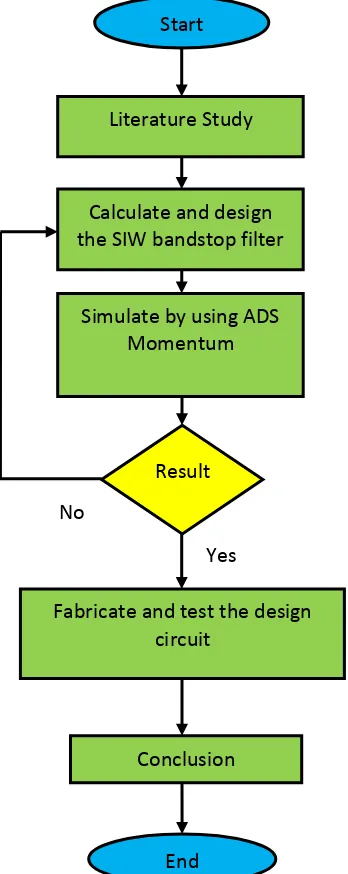
Start
Literature Study
Calculate and design the SIW bandstop filter
Simulate by using ADS Momentum
Fabricate and test the design circuit
Result
End Conclusion No
Yes
1.5 METHODOLOGY
This project start with literature study and research of the functions of SIW
and others topic that related to this project. This literature study is done by find out
all the journal, articles and books that related to this project either in website or any
other materials. Next, all the process to setup ADS momentum, and the flow on how
to run the simulation were learned. From the simulation, the bandstop response for
[image:20.612.256.430.255.692.2]SIW banstop filter is observed. Lastly, the design filter was fabricated and tested.
6
1.6 REPORT STRUCTURE
This report consists of chapters that will explain and discuss more details about
this project. This report was divided into 5 chapters. The first chapter gives a brief
explaination about Substrate Integrated Waveguide (SIW). It also gives an introduction
about the overall process of project.
Second chapter is about the literature review of the project. Background
knowledge of SIW and its components. The literature review helps to understand the
basic fundamental of this project.
Third chapter will explain about the project methodology. It gives details about
the methods used and all the process involved in this project.
Fourth chapter is about the result and discussion of this project, finding the
analysis throughout the research and project development. All the data and results that
obtained during this project will be documented in this chapter.
Lastly, fifth chapter is about the conclusion of this project. This chapter rounds
up the attained achievement of the whole project and reserves suggestions for possible
7
CHAPTER II
LITERATURE REVIEW
2.1 INTRODUCTION
Microwave filters are vital components in a huge variety of electronic system,
including cellular radio, satellite communications and radar. The specifications on these
devices are usually severe, often approaching the limit of what is theoretically
achievable in terms of frequency selectivity and phase linearity. However, knowledge of
network synthesis is not the only tool needed in order to design filters. Synthesis
provides the designer with a prototype network which can then be transformed into a
variety of microwave networks including TEM transmission lines, waveguides and
dielectric resonator realizations [13].
2.2 RF AND MICROWAVE FILTER
Microwave systems have an enormous impact on modern society. Applications
are diverse, from entertainment via satellite television, to civil and military radar
systems. Radar systems are used for detecting and locating air, ground or sea going
8
avoidance systems, weather forecast, motion detectors and a wide variety of remote
sensing systems. Microwave and RF filters are widely used in all these systems in order
to discriminate between wanted and unwanted signal frequencies. Cellular radio
provides particularly stringent filter requirements both in the base stations and in mobile
[image:23.612.162.527.194.384.2]handset. A typical filtering application is shown in Figure 2.1. [13]
Figure 2.1: RF front end of a cellular base station [13]
2.3 INTRODUCTION OF SUBSTRATE INTEGRATED WAVEDUIDE (SIW)
Nowadays, the quick development of the high-performance of microwave and
millimeter-wave communication systems influences the high-demand of this technology.
SIW which is based on planar dielectric substrates with top and bottom metal layers
perforated with metalized holes. It provides a compact size, low-cost, sharp selectivity
and low insertion loss for integrating active circuits, passive components and radiating
elements on the same substrate. Among these are the substrate integrated waveguides
(SIWs), initially introduced as laminated waveguides [1, 2], that can be easily
implemented using common printed circuit board (PCB) fabrication methods. Since the
9
interconnects, and circuits have been developed and their advantages are justified in
comparison to their milled waveguide or transmission line based counterparts.
As interconnects, it is seen that the substrate integrated waveguide (SIW)
interconnects provide a broadband bandpass signaling medium with excellent isolation
of electromagnetic interference (EMI) [18], while planar conventional transmission lines
are known as the performance bottleneck in ultra wideband systems due to their limited
bandwidth and high-frequency losses. In an SIW, the electric field distribution fills the
volume inside the waveguide interconnect and surface currents propagate on the larger
total cross-sectional area of the waveguide walls, resulting in lower conductor losses
[19]. As clock frequencies and circuit densities continue to increase, closely spaced
microstrip and stripline interconnects will no longer be viable options for
interconnection of system modules due to their open structure and increased
susceptibility to crosstalk and EMI.
SIWs, as a new means of signal transmission, have been the basis for the design
of many circuit components. Components such as power dividers, resonator cavities, and
filters that have been developed using microstrip, stripline or milled-waveguide
technologies are now redesigned using the SIW platform. The criticism that has been
raised about these new interconnects and components are that they possess a relatively
large footprint. Research works published in [7], [20] have in particular focused on the
development of waveguide miniaturization methods.
Various types of SIW power dividers, couplers, and diplexers have been
designed and optimized for operation at microwave and mm-wave frequency bands
using PCB substrates [21]. Other SIW-based components like waveguide cavities have
also been integrated directly into a PCB platform, allowing significant cost reduction in
the development and mass production of resonator based microwave oscillators and
filters. The high quality factor of the waveguide cavities provides excellent frequency
selectivity for cavity coupled filters and resonators [22]. The frequency selectivity of
![Figure 2.1: RF front end of a cellular base station [13]](https://thumb-ap.123doks.com/thumbv2/123dok/595681.71126/23.612.162.527.194.384/figure-rf-end-cellular-base-station.webp)
