Nama : Yusak Andre Setia
NRP :
0622041
Jurusan Teknik Elektro, Fakultas Teknik, Universitas Kristen Maranatha
Jl. Prof. Drg. Suria Sumantri,MPH. no. 65, Bandung, Indonesia
Email :
ABSTRAK
Penggunaan POV (Persistence Of Vision) biasanya digunakan sebagai
suatu alat untuk fungsi hiburan, ternyata juga bisa menampilkan suatu tampilan
untuk memperkenalkan suatu produk tertentu sesuai dengan program yang telah
diciptakan. Umumnya POV tidak dapat diprogram sesuai keinginan pengguna,
timbul gagasan untuk membuat sebuah POV yang dapat dengan mudah diprogram
sesuai keinginan.
Pada tugas akhir ini dirancang suatu perangkat berbasis mikrokontroler
Atmega 8 sebagai pengendali LED pada POV serta Atmega 16 sebagi pengendali
motor untuk POV. Pada tugas akhir ini juga ditampilkan 4 macam tampilan yang
berbeda sesuai dengan program yang telah terlebih dahulu dimasukan dalam
mikrokontroler Atmega 8. Tampilan dapat berubah secara offline sesuai dengan
kombinasi switch yang tersedia.
Dari hasil uji coba tampilan terlihat baik pada duty cycle=51,63%
(kecepatan=960 rpm + 2%) untuk POV dengan LED 3mm, sedangkan tampilan
akan terlihat baik pada duty cycle=45,63% (kecepatan 815 rpm + 3%) untuk POV
dengan LED 5mm.
DESIGN AND REALIZATION PROGRAMMABLE
POV (PERSISTENCE OF VISION) BY USING
A MICROCONTROLLER ATMEGA 8
Nama : Yusak Andre Setia
NRP :
0622041
Department of Electrical Engineering, Maranatha Christian University
Jl. Prof. Drg. Suria Sumantri,MPH. no. 65, Bandung, Indonesia
Email :
ABSTRACT
The use of POV (Persistence Of Vision) is usually used as a tool for
entertainment functions, it also can display an appearance to introduce a specific
product in accordance with a program that has been created. POV generally can
not be programmed according to user desires, the idea to create a POV that can
easily be programmed as desired.
In this final project, designed a device based on microcontroller Atmega 8
as controller LEDs on the POV and the Atmega 16 as a motor controller for the
POV. In this final project also featured four different kinds of view according to
the programs that have been first included in the microcontroller Atmega 8. Views
can change it offline in accordance with a combination of switches that are
available.
From the test results, POV display will look good on the duty cycle =
51.63% (speed = 960 rpm + 2%) for the POV with LED 3mm, and the display
will look good on the duty cycle = 45.63% (speed 815 rpm + 3%) for the POV
Halaman
ABSTRAK ...
i
ABSTRACT ...
ii
KATA PENGANTAR ...
iii
DAFTAR ISI ...
v
DAFTAR GAMBAR ...
viii
DAFTAR TABEL ...
xi
DAFTAR RUMUS ...
xii
BAB I
PENDAHULUAN
I.1 Latar Belakang ...
1
I.2 Perumusan Masalah ...
1
I.3 Tujuan ...
1
I.4 Pembatasan Masalah ...
2
I.5 Sistematika Penulisan ...
2
BAB II
LANDASAN TEORI
II.1 Pengertian POV (Persistence Of Vision) ...
4
II.2 Jenis-jenis Animasi ... 4
II.2.1 Animasi Stop-motion ...
5
II.2.2 Animasi Tradisional (Traditional animation) ...
5
II.2.3 Animasi komputer ...
6
II.3 Scanning pada Sistem POV ...
6
II.4 Mikrokontroler ...
7
II.4.1 Mikrokontroler Atmega 8 ...
7
II.4.1.1 Struktur Atmega 8 ...
8
II.4.1.2 Konfigurasi Pin Atmega 8 ...
9
II.4.2 Mikrokontroler Atmega 16 ...
11
II.4.2.2 Konfigurasi Pin Atmega 16 ...
13
II.4.2.3 Register dan Memori Atmega 16 ...
15
II.4.2.4 Timer ...
18
II.4.2.4.1 Timer/Counter1 ...
18
II.4.2.4.2 Register-register timer/counter1 ...
19
II.4.2.4.3 Prescaler ...
20
II.4.2.4.4 Mode Operasi ...
20
II.4.2.5 ADC ...
24
II.4.2.5.1 Mode Operasi ...
26
II.4.2.5.1.1 Mode konversi Tunggal ...
26
II.4.2.5.1.2 Mode free-running ...
26
BAB III PERANCANGAN SISTEM
III.1 Blok Diagram POV ...
27
III.1.1 Pengendali LED pada POV ...
27
III.1.1.1 Atmega 8 ...
28
III.1.1.2 Kombinasi Switch ...
30
III.1.2 Pengendali Motor untuk POV ...
32
BAB IV Data Pengamatan
IV.1 Pengujian Tampilan Huruf dan Angka ...
33
IV.2 Pengujian Tampilan dengan Perubahan Kombinasi 2 Buah Switch .
36
IV.2.1 Tampilan Kombinasi Pertama (“YUSAK”) ...
36
IV.2.2 Tampilan Kombinasi Kedua (“UKM 2010”) ...
37
IV.2.3 Tampilan Kombinasi Ketiga (“ELEKTRO”) ...
37
IV.2.4 Tampilan Kombinasi Keempat (“MARANATHA”) ...
38
IV.3 Pengujian Tampilan Dengan LED 5mm ...
38
DAFTAR PUSTAKA ...
45
LAMPIRAN A KODE PROGRAM
LAMPIRAN B FOTO ALAT
LAMPIRAN C KOMBINASI KARAKTER
LAMPIRAN D SKEMATIK RANGKAIAN
DAFTAR GAMBAR
Gambar 2.1 Proses gerakan berjalan pada animasi tradisional ...
5
Gambar 2.2 Proses Scanning pada POV ...
6
Gambar 2.3 Chip Atmega 8 ...
8
Gambar 2.4 Konfigurasi Pin Atmega 8 ...
9
Gambar 2.5 Diagram blok Atmega 8 ...
11
Gambar 2.6 Chip Atmega 16 ...
12
Gambar 2.7 Konfigurasi Pin Atmega 16 ...
13
Gambar 2.8 General Purpose Register Atmega 16 ...
15
Gambar 2.9 Pemetaan Memory Atmega 16 ...
16
Gambar 2.10 Diagram blok Timer1 ...
19
Gambar 2.11 Pulsa fast PWM ...
22
Gambar 2.12 Pulsa Phase Correct PWM ...
23
Gambar 3.1 Pengendali LED pada POV ...
27
Gambar 3.2 Pengendali Motor untuk POV ...
27
Gambar 3.3 Skema Rangkaian Pengendali LED pada POV ...
28
Gambar 3.4 Contoh penggunaan 7 buah LED pada POV yang
Menampilkan A2 ...
29
Gambar 3.5 Diagram Alir Pengendali LED pada POV ...
30
Gambar 3.6 Contoh Perancangan Tampilan A2 ...
31
Gambar 3.7 Skema Rangkaian Pengendali Motor untuk POV ...
34
Gambar 4.1 (a) Tangkapan Gambar A-D pada Tampilan Huruf A-I ...
35
Gambar 4.1 (b) Tangkapan Gambar B-E pada Tampilan Huruf A-I ...
35
Gambar 4.1 (c) Tangkapan Gambar F-I pada Tampilan Huruf A-I ...
36
Gambar 4.2 (a) Tangkapan Gambar J-M pada Tampilan Huruf J-R ...
36
Gambar 4.4 (b) Tangkapan Gambar 5,6 pada Tampilan Angka 1-9 ...
37
Gambar 4.4 (c) Tangkapan Gambar 6-9 pada Tampilan Angka 1-9 ...
38
Gambar 4.5 (a) Tangkapan Gambar YUSA pada Tampilan
Tulisan “YUSAK” ...
38
Gambar 4.5 (b) Tangkapan Gambar USAK pada Tampilan
Tulisan “YUSAK” ...
38
Gambar 4.6 (a) Tangkapan Gambar UKM pada Tampilan
Tulisan “UKM 2010” ...
39
Gambar 4.6 (b) Tangkapan Gambar 2010 pada Tampilan
Tulisan “UKM 2010” ...
39
Gambar 4.7 (a) Tangkapan Gambar ELEK pada Tampilan
Tulisan “ELEKTRO” ...
39
Gambar 4.7 (b) Tangkapan Gambar KTRO pada Tampilan
Tulisan “ELEKTRO” ...
39
Gambar 4.8 (a) Tangkapan Gambar MARA pada Tampilan
Tulisan “MARANATHA” ...
40
Gambar 4.8 (b) Tangkapan Gambar ARAN pada Tampilan
Tulisan “MARANATHA” ...
40
Gambar 4.8 (c) Tangkapan Gambar ATHA pada Tampilan
Tulisan “MARANATHA” ...
40
Gambar 4.9 Tampilan Tulisan “YUSAK” ...
41
Gambar 4.10 (a)Tangkapan Gambar UKM pada Tampilan
Tulisan “UKM 2010” ...
41
Gambar 4.10 (b)Tangkapan Gambar 2010 pada Tampilan
Gambar 4.11 (a)Tangkapan Gambar ELEKT pada Tampilan
Tulisan “ELEKTRO” ...
42
Gambar 4.11 (b)Tangkapan Gambar TRO pada Tampilan
Tulisan “ELEKTRO” ...
42
Gambar 4.12 (a)Tangkapan Gambar MARAN pada Tampilan
Tulisan “MARANATHA” ...
42
Gambar 4.12 (b)Tangkapan Gambar NATHA pada Tampilan
Tabel 2.1 Fungsi Khusus Port B Atmega 16 ...
14
Tabel 2.2 Fungsi Khusus Port C Atmega 16 ...
14
Tabel 2.3 Fungsi Khusus Port D Atmega 16...
14
Tabel 2.4 Pengalamatan Register I/O...
17
Tabel 3.1 SettingKonfigurasi Pengendali LED pada POV ...
28
Tabel 3.2 Setting Konfigurasi Pengendali Motor untuk POV ...
34
LAMPIRAN A
Pengendali Motor POV
/******************************* **********************
This program was produced by the CodeWizardAVR V1.25.3
Professional
Automatic Program Generator © Copyright 1998-2007 Pavel Haiduc, HP InfoTech s.r.l. http://www.hpinfotech.com
Project : Version :
Date : 11/22/2010 Author :
Company : Comments:
Chip type : ATmega16 Program type :
Application
Clock frequency : 11.059200 MHz
Memory model : Small External SRAM size : 0 Data Stack size : 256 ******************************** *********************/ #include <mega16.h> #include <stdio.h> #include <delay.h> char text[16]; char text2[16]; int var;
// Alphanumeric LCD Module functions
#asm
.equ __lcd_port=0x15 ;PORTC #endasm
#include <lcd.h>
#define ADC_VREF_TYPE 0x40
// Read the AD conversion result unsigned int read_adc(unsigned char adc_input)
{
ADMUX=adc_input | (ADC_VREF_TYPE
void main(void) {
// Declare your local variables here
// Input/Output Ports initialization
// Port A initialization // Func7=In Func6=In Func5=In Func4=In Func3=In Func2=In Func1=In Func0=In
// State7=T State6=T State5=T State4=T State3=T State2=T State1=T State0=T
PORTA=0x00; DDRA=0x00;
// Port B initialization // Func7=In Func6=In Func5=In Func4=In Func3=In Func2=In Func1=In Func0=In
// State7=T State6=T State5=T State4=T State3=T State2=T State1=T State0=T
PORTB=0x00; DDRB=0x00;
// Port C initialization // Func7=In Func6=In Func5=In Func4=In Func3=In Func2=In Func1=In Func0=In
// State7=T State6=T State5=T State4=T State3=T State2=T State1=T State0=T
PORTC=0x00; DDRC=0x00;
// Port D initialization // Func7=In Func6=In Func5=Out Func4=In Func3=In Func2=In Func1=In Func0=In
// State7=T State6=T State5=0 State4=T State3=T State2=T State1=T State0=T
PORTD=0x00; DDRD=0xFF;
// Timer/Counter 0 initialization
// Clock source: System Clock // Clock value: Timer 0 Stopped // Mode: Normal top=FFh
// OC0 output: Disconnected TCCR0=0x00;
Off // TCCR1A=0x80; // TCCR1B=0x15; // TCNT1H=0x00; // TCNT1L=0x00; // ICR1H=0xAF; // ICR1L=0x80; // OCR1AH=0x00; // OCR1AL=0x00; // OCR1BH=0x00; // OCR1BL=0x00;
// Timer/Counter 1 initialization
// Clock source: System Clock // Clock value: 1382.400 kHz // Mode: Ph. & fr. cor. PWM top=ICR1
// OC1A output: Non-Inv. // OC1B output: Discon. // Noise Canceler: Off
// Input Capture on Falling Edge // Timer 1 Overflow Interrupt: Off
// Input Capture Interrupt: Off // Compare A Match Interrupt: Off
// Compare B Match Interrupt: Off TCCR1A=0x80; TCCR1B=0x12; TCNT1H=0x00; TCNT1L=0x00; ICR1H=0xAF; ICR1L=0x80; OCR1AH=0x00; OCR1AL=0x00; OCR1BH=0x00; OCR1BL=0x00;
// Timer/Counter 2 initialization
// Clock source: System Clock // Clock value: Timer 2 Stopped // Mode: Normal top=FFh
// OC2 output: Disconnected ASSR=0x00;
TCCR2=0x00; TCNT2=0x00; OCR2=0x00;
// External Interrupt(s) initialization
// INT0: Off // INT1: Off // INT2: Off MCUCR=0x00; MCUCSR=0x00;
// Timer(s)/Counter(s) Interrupt(s) initialization TIMSK=0x00;
// Analog Comparator
// ADC initialization
// ADC Clock frequency: 691.200 kHz
// ADC Voltage Reference: AVCC pin
// ADC Auto Trigger Source: Free Running
ADMUX=ADC_VREF_TYPE & 0xff; ADCSRA=0xA4;
SFIOR&=0x1F;
// LCD module initialization lcd_init(16);
read_adc(0);
while (1) {
// Place your code here var=ADCW; OCR1A=10000+var*35; lcd_clear(); sprintf(text,"ocr=%5u",OCR1A); sprintf(text2,"adc=%4u",var); lcd_puts(text); lcd_gotoxy(0,1); lcd_puts(text2); delay_ms(100); }; }
Pengendali LED POV
/******************************* **********************
This program was produced by the CodeWizardAVR V2.03.7 Evaluation Automatic Program Generator © Copyright 1998-2008 Pavel Haiduc, HP InfoTech s.r.l. http://www.hpinfotech.com
Project : Version :
Date : 12/3/2010 Author : Freeware, for evaluation and non-commercial use only
Company : Comments:
Chip type : ATmega8 Program type :
Application
External RAM size : 0 Data Stack size : 256 ******************************** *********************/
#include <mega8.h> #include <delay.h>
// Declare your global variables here
int hit;
void main(void) {
// Declare your local variables here
// Input/Output Ports initialization
// Port B initialization // Func7=In Func6=In Func5=In Func4=In Func3=In Func2=In Func1=In Func0=Out
// State7=T State6=T State5=T State4=T State3=T State2=T State1=T State0=0
PORTB=0x01; DDRB=0x01;
// Port C initialization // Func6=In Func5=Out Func4=In Func3=Out Func2=In Func1=In Func0=In
// State6=T State5=0 State4=T State3=0 State2=T State1=T State0=T
PORTC=0x78; DDRC=0x28;
// Port D initialization
// Func7=Out Func6=Out Func5=Out Func4=Out Func3=Out Func2=Out Func1=Out Func0=Out
// State7=0 State6=0 State5=0 State4=0 State3=0 State2=0 State1=0 State0=0
PORTD=0x00; DDRD=0xFF;
// Timer/Counter 0 initialization
// Clock source: System Clock // Clock value: Timer 0 Stopped TCCR0=0x00;
TCNT0=0x00;
// Timer/Counter 1 initialization
// Clock source: System Clock
TCCR1A=0x00; TCCR1B=0x00; TCNT1H=0x00; TCNT1L=0x00; ICR1H=0x00; ICR1L=0x00; OCR1AH=0x00; OCR1AL=0x00; OCR1BH=0x00; OCR1BL=0x00;
// Timer/Counter 2 initialization
// Clock source: System Clock // Clock value: Timer 2 Stopped // Mode: Normal top=FFh
// OC2 output: Disconnected ASSR=0x00;
TCCR2=0x00; TCNT2=0x00; OCR2=0x00;
// External Interrupt(s) initialization
// INT0: Off // INT1: Off MCUCR=0x00;
// Timer(s)/Counter(s) Interrupt(s) initialization TIMSK=0x00;
// Analog Comparator initialization
// Analog Comparator: Off // Analog Comparator Input Capture by Timer/Counter 1: Off ACSR=0x80;
SFIOR=0x00;
while (1) {
if (PINC.3==1 && PINC.5==1)
{
if (PINB.0==0) {
PORTD=0x7c;
PORTD=0x01; delay_ms(1); PORTD=0x7f; delay_ms(1); PORTD=0x01; delay_ms(1); PORTD=0x01; delay_ms(1); PORTD=0x00; delay_ms(2); PORTD=0x7c;
delay_ms(1); //A PORTD=0x0a; delay_ms(1); PORTD=0x09; delay_ms(1); PORTD=0x0a; delay_ms(1); PORTD=0x7c; delay_ms(1); PORTD=0x00; delay_ms(2); PORTD=0x7f;
delay_ms(1); //N PORTD=0x10; delay_ms(1); PORTD=0x08; delay_ms(1); PORTD=0x04; delay_ms(1); PORTD=0x7f; delay_ms(1); PORTD=0x00; delay_ms(2); PORTD=0x7c;
delay_ms(1); //A PORTD=0x0a; delay_ms(1); PORTD=0x09; delay_ms(1); PORTD=0x0a; delay_ms(1); PORTD=0x7c; delay_ms(1); PORTD=0x00; delay_ms(2); PORTD=0x46;
delay_ms(1); //R PORTD=0x29; delay_ms(1); PORTD=0x19; delay_ms(1); PORTD=0x09; delay_ms(1); PORTD=0x7f; delay_ms(1); PORTD=0x00; delay_ms(2); PORTD=0x7c; delay_ms(1); PORTD=0x7c; delay_ms(1); PORTD=0x00; delay_ms(2); PORTD=0x7f;
delay_ms(1); //M PORTD=0x02; delay_ms(1); PORTD=0x0c; delay_ms(1); PORTD=0x02; delay_ms(1); PORTD=0x7f; delay_us(500); PORTD=0x00; delay_ms(4);hit=1; } else {PORTD=0x00 ; } }
if (PINC.3==0 && PINC.5==0)
{
if (PINB.0==0) {PORTD=0x41;
delay_ms(1); // K PORTD=0x22; delay_ms(1); PORTD=0x14; delay_ms(1); PORTD=0x08; delay_ms(1); PORTD=0x7f; delay_ms(1); PORTD=0x00; delay_ms(2); PORTD=0x7c;
delay_ms(1); //A PORTD=0x0a; delay_ms(1); PORTD=0x09; delay_ms(1); PORTD=0x0a; delay_ms(1); PORTD=0x7c; delay_ms(1); PORTD=0x00; delay_ms(2); PORTD=0x31;
delay_ms(1); PORTD=0x00; delay_ms(2);
PORTD=0x3f;
delay_ms(1); //U PORTD=0x40; delay_ms(1); PORTD=0x40; delay_ms(1); PORTD=0x40; delay_ms(1); PORTD=0x3f; delay_ms(1); PORTD=0x00; delay_ms(2); PORTD=0x07;
delay_ms(1); //Y PORTD=0x04; delay_ms(1); PORTD=0x7c; delay_ms(1); PORTD=0x04; delay_ms(1); PORTD=0x07; delay_ms(1); PORTD=0x00; delay_ms(2); PORTD=0x00;
delay_ms(1); //... PORTD=0x00; delay_ms(1); PORTD=0x00; delay_ms(1); PORTD=0x00; delay_ms(1); PORTD=0x00; delay_ms(1); PORTD=0x00; delay_ms(2); PORTD=0x00;
delay_ms(1); //... PORTD=0x00; delay_ms(1); PORTD=0x00; delay_ms(1); PORTD=0x00; delay_ms(1); PORTD=0x00; delay_ms(1); PORTD=0x00; delay_ms(2); PORTD=0x00;
delay_ms(1); //.. PORTD=0x00; delay_ms(1); PORTD=0x00; delay_ms(1); PORTD=0x00; delay_ms(1); PORTD=0x00; delay_us(500); PORTD=0x00; delay_ms(4); } else {PORTD=0x00 ; } }
if (PINC.3==1 && PINC.5==0)
{
if (PINB.0==0) {PORTD=0x3e;
delay_ms(1); // O PORTD=0x41; delay_ms(1); PORTD=0x41; delay_ms(1); PORTD=0x41; delay_ms(1); PORTD=0x3e; delay_ms(1); PORTD=0x00; delay_ms(2); PORTD=0x46;
delay_ms(1); // R PORTD=0x29; delay_ms(1); PORTD=0x19; delay_ms(1); PORTD=0x09; delay_ms(1); PORTD=0x7f; delay_ms(1); PORTD=0x00; delay_ms(2); PORTD=0x01;
delay_ms(1); //E PORTD=0x49; delay_ms(1); PORTD=0x49; delay_ms(1); PORTD=0x49; delay_ms(1); PORTD=0x7f; delay_ms(1); PORTD=0x00; delay_ms(2); PORTD=0x40;
delay_ms(1); //L PORTD=0x40; delay_ms(1); PORTD=0x40; delay_ms(1); PORTD=0x40; delay_ms(1); PORTD=0x7f; delay_ms(1); PORTD=0x00; delay_ms(2); PORTD=0x41;
delay_ms(1); //E PORTD=0x49; delay_ms(1); PORTD=0x49; delay_ms(1); PORTD=0x49; delay_ms(1); PORTD=0x7f; delay_ms(1); PORTD=0x00; delay_ms(2); PORTD=0x00;
delay_ms(1); //... PORTD=0x00; delay_ms(1); PORTD=0x00; delay_ms(1); PORTD=0x00; delay_ms(1); PORTD=0x00; delay_ms(1); PORTD=0x00; delay_ms(2); PORTD=0x00;
delay_ms(1); //.. PORTD=0x00; delay_ms(1); PORTD=0x00; delay_ms(1); PORTD=0x00; delay_ms(1); PORTD=0x00; delay_us(500); PORTD=0x00; delay_ms(4); } PINC.5==1) { if (PINB.0==0) {PORTD=0x3e;
delay_ms(1); // 0 PORTD=0x45; delay_ms(1); PORTD=0x49; delay_ms(1); PORTD=0x51; delay_ms(1); PORTD=0x3e; delay_ms(1); PORTD=0x00; delay_ms(2); PORTD=0x40;
delay_ms(1); // 1 PORTD=0x7f; delay_ms(1); PORTD=0x42; delay_ms(1); PORTD=0x00; delay_ms(2); PORTD=0x3e;
delay_ms(1); // 0 PORTD=0x45; delay_ms(1); PORTD=0x49; delay_ms(1); PORTD=0x51; delay_ms(1); PORTD=0x3e; delay_ms(1); PORTD=0x00; delay_ms(2); PORTD=0x46;
delay_ms(1); //2 PORTD=0x49; delay_ms(1); PORTD=0x51; delay_ms(1); PORTD=0x61; delay_ms(1); PORTD=0x42; delay_ms(1); PORTD=0x00; delay_ms(4); PORTD=0x7f;
delay_ms(1); //K PORTD=0x22; delay_ms(1); PORTD=0x14; delay_ms(1); PORTD=0x08; delay_ms(1); PORTD=0x7f; delay_ms(1); PORTD=0x00; delay_ms(2); PORTD=0x3f;
delay_ms(1); //U PORTD=0x40; delay_ms(1); PORTD=0x40; delay_ms(1); PORTD=0x40; delay_ms(1); PORTD=0x3f; delay_ms(1); PORTD=0x00; delay_ms(2); PORTD=0x00;
delay_ms(1); //... PORTD=0x00; delay_ms(1); PORTD=0x00; delay_ms(1); PORTD=0x00; delay_ms(1); PORTD=0x00; delay_ms(1); PORTD=0x00; delay_ms(2); PORTD=0x00;
LAMPIRAN B
LAMPIRAN C
LAMPIRAN C
LAMPIRAN E
DATASHEET
---IC Atmega 8 ………
E-1
IC Atmega 16 ………
E-18
IC L293D ………
E-41
LCD ………
E-45
LAMPIRAN D
SKEMATIK RANGKAIAN
---PENGENDALI LED PADA POV
………
D-1
PENGENDALI MOTOR UNTUK POV
……
D-2
2486Q–AVR–10/06 – 32 x 8 General Purpose Working Registers
– Fully Static Operation
– Up to 16 MIPS Throughput at 16 MHz – On-chip 2-cycle Multiplier
• Nonvolatile Program and Data Memories
– 8K Bytes of In-System Self-Programmable Flash Endurance: 10,000 Write/Erase Cycles
– Optional Boot Code Section with Independent Lock Bits In-System Programming by On-chip Boot Program True Read-While-Write Operation
– 512 Bytes EEPROM
Endurance: 100,000 Write/Erase Cycles – 1K Byte Internal SRAM
– Programming Lock for Software Security • Peripheral Features
– Two 8-bit Timer/Counters with Separate Prescaler, one Compare Mode
– One 16-bit Timer/Counter with Separate Prescaler, Compare Mode, and Capture Mode
– Real Time Counter with Separate Oscillator – Three PWM Channels
– 8-channel ADC in TQFP and QFN/MLF package Eight Channels 10-bit Accuracy
– 6-channel ADC in PDIP package Eight Channels 10-bit Accuracy – Byte-oriented Two-wire Serial Interface – Programmable Serial USART
– Master/Slave SPI Serial Interface
– Programmable Watchdog Timer with Separate On-chip Oscillator – On-chip Analog Comparator
• Special Microcontroller Features
– Power-on Reset and Programmable Brown-out Detection – Internal Calibrated RC Oscillator
– External and Internal Interrupt Sources
– Five Sleep Modes: Idle, ADC Noise Reduction, Power-save, Power-down, and Standby
• I/O and Packages
– 23 Programmable I/O Lines
– 28-lead PDIP, 32-lead TQFP, and 32-pad QFN/MLF • Operating Voltages
– 2.7 - 5.5V (ATmega8L) – 4.5 - 5.5V (ATmega8)
• Speed Grades
– 0 - 8 MHz (ATmega8L) – 0 - 16 MHz (ATmega8)
• Power Consumption at 4 Mhz, 3V, 25°C – Active: 3.6 mA
– Idle Mode: 1.0 mA
– Power-down Mode: 0.5 µA
8-bit
with 8K Bytes
In-System
Programmable
Flash
Pin Configurations
1 2 3 4 5 6 7 8 24 23 22 21 20 19 18 17 (INT1) PD3 (XCK/T0) PD4 GND VCC GND VCC (XTAL1/TOSC1) PB6 (XTAL2/TOSC2) PB7 PC1 (ADC1) PC0 (ADC0) ADC7 GND AREF ADC6 AVCC PB5 (SCK)32 31 30 29 28 27 26 25
9 10 11 12 13 14 15 16
(T1) PD5
(AIN0) PD6 (AIN1) PD7 (ICP1) PB0 (OC1A) PB1 (SS/OC1B) PB2 (MOSI/OC2) PB3
(MISO) PB4
PD2 (INT0) PD1 (TXD) PD0 (RXD) PC6 (RESET) PC5 (ADC5/SCL) PC4 (ADC4/SDA) PC3 (ADC3) PC2 (ADC2) TQFP Top View
1 2 3 4 5 6 7 8 9 10 11 12 13 14 28 27 26 25 24 23 22 21 20 19 18 17 16 15 (RESET) PC6 (RXD) PD0 (TXD) PD1 (INT0) PD2 (INT1) PD3 (XCK/T0) PD4 VCC GND (XTAL1/TOSC1) PB6 (XTAL2/TOSC2) PB7 (T1) PD5 (AIN0) PD6 (AIN1) PD7 (ICP1) PB0 PC5 (ADC5/SCL) PC4 (ADC4/SDA) PC3 (ADC3) PC2 (ADC2) PC1 (ADC1) PC0 (ADC0) GND AREF AVCC PB5 (SCK) PB4 (MISO) PB3 (MOSI/OC2) PB2 (SS/OC1B) PB1 (OC1A) PDIP 1 2 24 23
32 31 30 29 28 27 26 25 MLF Top View
(INT1) PD3 (XCK/T0) PD4
PC1 (ADC1) PC0 (ADC0)
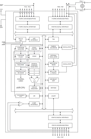
Overview
The ATmega8 is a low-power CMOS 8-bit microcontroller based on the AVR RISC architecture. By executing powerful instructions in a single clock cycle, the ATmega8 achieves throughputs approaching 1 MIPS per MHz, allowing the system designer to optimize power consumption versus processing speed.Block Diagram
Figure 1. Block DiagramINTERNAL OSCILLATOR OSCILLATOR WATCHDOG TIMER MCU CTRL. & TIMING OSCILLATOR TIMERS/ COUNTERS INTERRUPT UNIT STACK POINTER EEPROM SRAM STATUS REGISTER USART PROGRAM COUNTER PROGRAM FLASH INSTRUCTION REGISTER INSTRUCTION DECODER PROGRAMMING LOGIC SPI ADC INTERFACE COMP. INTERFACE PORTC DRIVERS/BUFFERS
PORTC DIGITAL INTERFACE
GENERAL PURPOSE REGISTERS X Y Z ALU + -PORTB DRIVERS/BUFFERS
PORTB DIGITAL INTERFACE
PORTD DIGITAL INTERFACE
PORTD DRIVERS/BUFFERS XTAL1 XTAL2 CONTROL LINES VCC GND MUX & ADC AGND AREF
PC0 - PC6 PB0 - PB7
PD0 - PD7
AVR CPU
[image:31.612.203.563.148.697.2]The AVR core combines a rich instruction set with 32 general purpose working registers. All the 32 registers are directly connected to the Arithmetic Logic Unit (ALU), allowing two independent registers to be accessed in one single instruction executed in one clock cycle. The resulting architecture is more code efficient while achieving throughputs up to ten times faster than conventional CISC microcontrollers.
The ATmega8 provides the following features: 8K bytes of In-System Programmable Flash with Read-While-Write capabilities, 512 bytes of EEPROM, 1K byte of SRAM, 23 general purpose I/O lines, 32 general purpose working registers, three flexible Timer/Counters with compare modes, internal and external interrupts, a serial program-mable USART, a byte oriented Two-wire Serial Interface, a 6-channel ADC (eight channels in TQFP and QFN/MLF packages) with 10-bit accuracy, a programmable Watchdog Timer with Internal Oscillator, an SPI serial port, and five software selectable power saving modes. The Idle mode stops the CPU while allowing the SRAM, Timer/Counters, SPI port, and interrupt system to continue functioning. The Power-down mode saves the register contents but freezes the Oscillator, disabling all other chip functions until the next Interrupt or Hardware Reset. In Power-save mode, the asynchronous timer continues to run, allowing the user to maintain a timer base while the rest of the device is sleeping. The ADC Noise Reduction mode stops the CPU and all I/O modules except asynchronous timer and ADC, to minimize switching noise during ADC conversions. In Standby mode, the crystal/resonator Oscillator is running while the rest of the device is sleeping. This allows very fast start-up combined with low-power consumption.
The device is manufactured using Atmel’s high density non-volatile memory technology. The Flash Program memory can be reprogrammed In-System through an SPI serial interface, by a conventional non-volatile memory programmer, or by an On-chip boot program running on the AVR core. The boot program can use any interface to download the application program in the Application Flash memory. Software in the Boot Flash Section will continue to run while the Application Flash Section is updated, providing true Read-While-Write operation. By combining an 8-bit RISC CPU with In-System Self-Programmable Flash on a monolithic chip, the Atmel ATmega8 is a powerful microcon-troller that provides a highly-flexible and cost-effective solution to many embedded control applications.
The ATmega8 AVR is supported with a full suite of program and system development tools, including C compilers, macro assemblers, program debugger/simulators, In-Cir-cuit Emulators, and evaluation kits.
Pin Descriptions
VCC Digital supply voltage.
GND Ground.
Port B (PB7..PB0)
XTAL1/XTAL2/TOSC1/TOSC2
Port B is an 8-bit bi-directional I/O port with internal pull-up resistors (selected for each bit). The Port B output buffers have symmetrical drive characteristics with both high sink and source capability. As inputs, Port B pins that are externally pulled low will source current if the pull-up resistors are activated. The Port B pins are tri-stated when a reset condition becomes active, even if the clock is not running.
Depending on the clock selection fuse settings, PB6 can be used as input to the invert-ing Oscillator amplifier and input to the internal clock operatinvert-ing circuit.
Depending on the clock selection fuse settings, PB7 can be used as output from the inverting Oscillator amplifier.
If the Internal Calibrated RC Oscillator is used as chip clock source, PB7..6 is used as TOSC2..1 input for the Asynchronous Timer/Counter2 if the AS2 bit in ASSR is set.
The various special features of Port B are elaborated in “Alternate Functions of Port B” on page 58 and “System Clock and Clock Options” on page 25.
Port C (PC5..PC0) Port C is an 7-bit bi-directional I/O port with internal pull-up resistors (selected for each bit). The Port C output buffers have symmetrical drive characteristics with both high sink and source capability. As inputs, Port C pins that are externally pulled low will source current if the pull-up resistors are activated. The Port C pins are tri-stated when a reset condition becomes active, even if the clock is not running.
PC6/RESET If the RSTDISBL Fuse is programmed, PC6 is used as an I/O pin. Note that the
electri-cal characteristics of PC6 differ from those of the other pins of Port C.
If the RSTDISBL Fuse is unprogrammed, PC6 is used as a Reset input. A low level on this pin for longer than the minimum pulse length will generate a Reset, even if the clock is not running. The minimum pulse length is given in Table 15 on page 38. Shorter pulses are not guaranteed to generate a Reset.
The various special features of Port C are elaborated on page 61.
Port D (PD7..PD0) Port D is an 8-bit bi-directional I/O port with internal pull-up resistors (selected for each bit). The Port D output buffers have symmetrical drive characteristics with both high sink and source capability. As inputs, Port D pins that are externally pulled low will source current if the pull-up resistors are activated. The Port D pins are tri-stated when a reset condition becomes active, even if the clock is not running.
Port D also serves the functions of various special features of the ATmega8 as listed on page 63.
RESET Reset input. A low level on this pin for longer than the minimum pulse length will
AVCC AVCC is the supply voltage pin for the A/D Converter, Port C (3..0), and ADC (7..6). It should be externally connected to VCC, even if the ADC is not used. If the ADC is used, it should be connected to VCC through a low-pass filter. Note that Port C (5..4) use digital supply voltage, VCC.
AREF AREF is the analog reference pin for the A/D Converter.
ADC7..6 (TQFP and QFN/MLF Package Only)
About Code
Examples
AVR CPU Core
Introduction
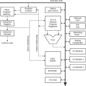
This section discusses the AVR core architecture in general. The main function of the CPU core is to ensure correct program execution. The CPU must therefore be able to access memories, perform calculations, control peripherals, and handle interrupts.Architectural Overview
Figure 2. Block Diagram of the AVR MCU ArchitectureIn order to maximize performance and parallelism, the AVR uses a Harvard architecture – with separate memories and buses for program and data. Instructions in the Program memory are executed with a single level pipelining. While one instruction is being exe-cuted, the next instruction is pre-fetched from the Program memory. This concept enables instructions to be executed in every clock cycle. The Program memory is In-System Reprogrammable Flash memory.
The fast-access Register File contains 32 x 8-bit general purpose working registers with a single clock cycle access time. This allows single-cycle Arithmetic Logic Unit (ALU) operation. In a typical ALU operation, two operands are output from the Register File, the operation is executed, and the result is stored back in the Register File – in one clock cycle.
Flash Program
Memory
Instruction Register
Instruction Decoder
Program Counter
Control Lines
32 x 8 General Purpose Registrers
ALU Status and Control
I/O Lines EEPROM
Data Bus 8-bit
Data SRAM
Direct Addressing Indirect Addressing
Interrupt Unit
SPI Unit
Watchdog Timer
Analog Comparator
i/O Module 2 i/O Module1
[image:37.612.220.571.188.540.2]Six of the 32 registers can be used as three 16-bit indirect address register pointers for Data Space addressing – enabling efficient address calculations. One of the these address pointers can also be used as an address pointer for look up tables in Flash Pro-gram memory. These added function registers are the 16-bit X-, Y-, and Z-register, described later in this section.
The ALU supports arithmetic and logic operations between registers or between a con-stant and a register. Single register operations can also be executed in the ALU. After an arithmetic operation, the Status Register is updated to reflect information about the result of the operation.
The Program flow is provided by conditional and unconditional jump and call instruc-tions, able to directly address the whole address space. Most AVR instructions have a single 16-bit word format. Every Program memory address contains a 16- or 32-bit instruction.
Program Flash memory space is divided in two sections, the Boot program section and the Application program section. Both sections have dedicated Lock Bits for write and read/write protection. The SPM instruction that writes into the Application Flash memory section must reside in the Boot program section.
During interrupts and subroutine calls, the return address Program Counter (PC) is stored on the Stack. The Stack is effectively allocated in the general data SRAM, and consequently the Stack size is only limited by the total SRAM size and the usage of the SRAM. All user programs must initialize the SP in the reset routine (before subroutines or interrupts are executed). The Stack Pointer SP is read/write accessible in the I/O space. The data SRAM can easily be accessed through the five different addressing modes supported in the AVR architecture.
The memory spaces in the AVRarchitecture are all linear and regular memory maps.
A flexible interrupt module has its control registers in the I/O space with an additional global interrupt enable bit in the Status Register. All interrupts have a separate Interrupt Vector in the Interrupt Vector table. The interrupts have priority in accordance with their Interrupt Vector position. The lower the Interrupt Vector address, the higher the priority.
Arithmetic Logic Unit –
ALU
The high-performance AVR ALU operates in direct connection with all the 32 general purpose working registers. Within a single clock cycle, arithmetic operations between general purpose registers or between a register and an immediate are executed. The ALU operations are divided into three main categories – arithmetic, logical, and bit-func-tions. Some implementations of the architecture also provide a powerful multiplier supporting both signed/unsigned multiplication and fractional format. See the “Instruc-tion Set” sec“Instruc-tion for a detailed descrip“Instruc-tion.
Status Register
The Status Register contains information about the result of the most recently executed arithmetic instruction. This information can be used for altering program flow in order to perform conditional operations. Note that the Status Register is updated after all ALU operations, as specified in the Instruction Set Reference. This will in many cases remove the need for using the dedicated compare instructions, resulting in faster and more compact code.The Status Register is not automatically stored when entering an interrupt routine and restored when returning from an interrupt. This must be handled by software.
The AVR Status Register – SREG – is defined as:
• Bit 7 – I: Global Interrupt Enable
The Global Interrupt Enable bit must be set for the interrupts to be enabled. The individ-ual interrupt enable control is then performed in separate control registers. If the Global Interrupt Enable Register is cleared, none of the interrupts are enabled independent of the individual interrupt enable settings. The I-bit is cleared by hardware after an interrupt has occurred, and is set by the RETI instruction to enable subsequent interrupts. The I-bit can also be set and cleared by the application with the SEI and CLI instructions, as described in the Instruction Set Reference.
• Bit 6 – T: Bit Copy Storage
The Bit Copy instructions BLD (Bit LoaD) and BST (Bit STore) use the T-bit as source or destination for the operated bit. A bit from a register in the Register File can be copied into T by the BST instruction, and a bit in T can be copied into a bit in a register in the Register File by the BLD instruction.
• Bit 5 – H: Half Carry Flag
The Half Carry Flag H indicates a Half Carry in some arithmetic operations. Half Carry is useful in BCD arithmetic. See the “Instruction Set Description” for detailed information. • Bit 4 – S: Sign Bit, S = N
⊕
VThe S-bit is always an exclusive or between the Negative Flag N and the Two’s Comple-ment Overflow Flag V. See the “Instruction Set Description” for detailed information. • Bit 3 – V: Two’s Complement Overflow Flag
The Two’s Complement Overflow Flag V supports two’s complement arithmetics. See the “Instruction Set Description” for detailed information.
• Bit 2 – N: Negative Flag
The Negative Flag N indicates a negative result in an arithmetic or logic operation. See the “Instruction Set Description” for detailed information.
• Bit 1 – Z: Zero Flag
Bit 7 6 5 4 3 2 1 0
I T H S V N Z C SREG
Read/Write R/W R/W R/W R/W R/W R/W R/W R/W
The Zero Flag Z indicates a zero result in an arithmetic or logic operation. See the “Instruction Set Description” for detailed information.
• Bit 0 – C: Carry Flag
The Carry Flag C indicates a Carry in an arithmetic or logic operation. See the “Instruc-tion Set Descrip“Instruc-tion” for detailed informa“Instruc-tion.
General Purpose
Register File
The Register File is optimized for the AVR Enhanced RISC instruction set. In order to achieve the required performance and flexibility, the following input/output schemes are supported by the Register File:
• One 8-bit output operand and one 8-bit result input. • Two 8-bit output operands and one 8-bit result input. • Two 8-bit output operands and one 16-bit result input. • One 16-bit output operand and one 16-bit result input.
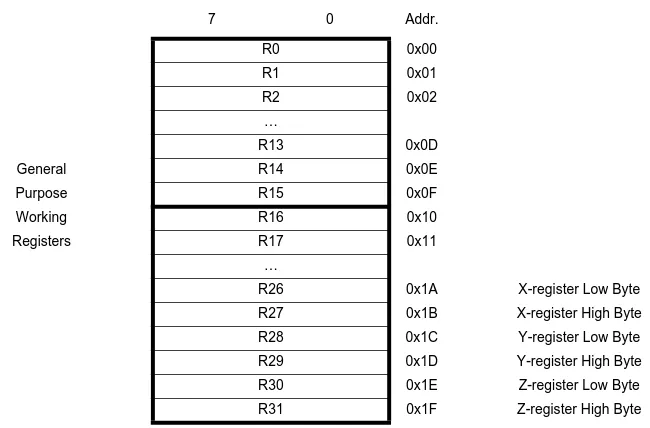
[image:40.612.224.549.300.514.2]Figure 3 shows the structure of the 32 general purpose working registers in the CPU.
Figure 3. AVR CPU General Purpose Working Registers
Most of the instructions operating on the Register File have direct access to all registers, and most of them are single cycle instructions.
As shown in Figure 3, each register is also assigned a Data memory address, mapping them directly into the first 32 locations of the user Data Space. Although not being phys-ically implemented as SRAM locations, this memory organization provides great flexibility in access of the registers, as the X-, Y-, and Z-pointer Registers can be set to
7 0 Addr.
R0 0x00
R1 0x01
R2 0x02
…
R13 0x0D
General R14 0x0E
Purpose R15 0x0F
Working R16 0x10
Registers R17 0x11
…
R26 0x1A X-register Low Byte
R27 0x1B X-register High Byte
R28 0x1C Y-register Low Byte
R29 0x1D Y-register High Byte
R30 0x1E Z-register Low Byte
The X-register, Y-register and Z-register
The registers R26..R31 have some added functions to their general purpose usage. These registers are 16-bit address pointers for indirect addressing of the Data Space. The three indirect address registers X, Y and Z are defined as described in Figure 4.
Figure 4. The X-, Y- and Z-Registers
In the different addressing modes these address registers have functions as fixed dis-placement, automatic increment, and automatic decrement (see the Instruction Set Reference for details).
Stack Pointer
The Stack is mainly used for storing temporary data, for storing local variables and for storing return addresses after interrupts and subroutine calls. The Stack Pointer Regis-ter always points to the top of the Stack. Note that the Stack is implemented as growing from higher memory locations to lower memory locations. This implies that a Stack PUSH command decreases the Stack Pointer.The Stack Pointer points to the data SRAM Stack area where the Subroutine and Inter-rupt Stacks are located. This Stack space in the data SRAM must be defined by the program before any subroutine calls are executed or interrupts are enabled. The Stack Pointer must be set to point above 0x60. The Stack Pointer is decremented by one when data is pushed onto the Stack with the PUSH instruction, and it is decremented by two when the return address is pushed onto the Stack with subroutine call or interrupt. The Stack Pointer is incremented by one when data is popped from the Stack with the POP instruction, and it is incremented by two when address is popped from the Stack with return from subroutine RET or return from interrupt RETI.
The AVR Stack Pointer is implemented as two 8-bit registers in the I/O space. The num-ber of bits actually used is implementation dependent. Note that the data space in some implementations of the AVR architecture is so small that only SPL is needed. In this case, the SPH Register will not be present.
15 XH XL 0
X-register 7 0 7 0
R27 (0x1B) R26 (0x1A)
15 YH YL 0
Y-register 7 0 7 0
R29 (0x1D) R28 (0x1C)
15 ZH ZL 0
Z-register 7 0 7 0
R31 (0x1F) R30 (0x1E)
Bit 15 14 13 12 11 10 9 8
SP15 SP14 SP13 SP12 SP11 SP10 SP9 SP8 SPH SP7 SP6 SP5 SP4 SP3 SP2 SP1 SP0 SPL
7 6 5 4 3 2 1 0
Read/Write R/W R/W R/W R/W R/W R/W R/W R/W
R/W R/W R/W R/W R/W R/W R/W R/W
Initial Value 0 0 0 0 0 0 0 0
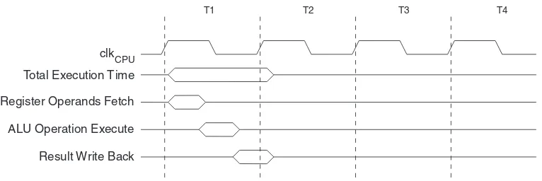
Instruction Execution
Timing
This section describes the general access timing concepts for instruction execution. The AVR CPU is driven by the CPU clock clkCPU, directly generated from the selected clock source for the chip. No internal clock division is used.
Figure 5 shows the parallel instruction fetches and instruction executions enabled by the Harvard architecture and the fast-access Register File concept. This is the basic pipelin-ing concept to obtain up to 1 MIPS per MHz with the correspondpipelin-ing unique results for functions per cost, functions per clocks, and functions per power-unit.
Figure 5. The Parallel Instruction Fetches and Instruction Executions
[image:42.612.193.576.409.537.2]Figure 6 shows the internal timing concept for the Register File. In a single clock cycle an ALU operation using two register operands is executed, and the result is stored back to the destination register.
Figure 6. Single Cycle ALU Operation
Reset and Interrupt
Handling
The AVR provides several different interrupt sources. These interrupts and the separate Reset Vector each have a separate Program Vector in the Program memory space. All interrupts are assigned individual enable bits which must be written logic one together
clk 1st Instruction Fetch 1st Instruction Execute 2nd Instruction Fetch 2nd Instruction Execute 3rd Instruction Fetch 3rd Instruction Execute 4th Instruction Fetch
T1 T2 T3 T4
CPU
Total Execution Time Register Operands Fetch ALU Operation Execute Result Write Back
T1 T2 T3 T4
of the boot Flash section by setting the Interrupt Vector Select (IVSEL) bit in the General Interrupt Control Register (GICR). Refer to “Interrupts” on page 46 for more information. The Reset Vector can also be moved to the start of the boot Flash section by program-ming the BOOTRST Fuse, see “Boot Loader Support – Read-While-Write Self-Programming” on page 209.
When an interrupt occurs, the Global Interrupt Enable I-bit is cleared and all interrupts are disabled. The user software can write logic one to the I-bit to enable nested inter-rupts. All enabled interrupts can then interrupt the current interrupt routine. The I-bit is automatically set when a Return from Interrupt instruction – RETI – is executed.
There are basically two types of interrupts. The first type is triggered by an event that sets the Interrupt Flag. For these interrupts, the Program Counter is vectored to the actual Interrupt Vector in order to execute the interrupt handling routine, and hardware clears the corresponding Interrupt Flag. Interrupt Flags can also be cleared by writing a logic one to the flag bit position(s) to be cleared. If an interrupt condition occurs while the corresponding interrupt enable bit is cleared, the Interrupt Flag will be set and remem-bered until the interrupt is enabled, or the flag is cleared by software. Similarly, if one or more interrupt conditions occur while the global interrupt enable bit is cleared, the corre-sponding Interrupt Flag(s) will be set and remembered until the global interrupt enable bit is set, and will then be executed by order of priority.
The second type of interrupts will trigger as long as the interrupt condition is present. These interrupts do not necessarily have Interrupt Flags. If the interrupt condition disap-pears before the interrupt is enabled, the interrupt will not be triggered.
When the AVR exits from an interrupt, it will always return to the main program and exe-cute one more instruction before any pending interrupt is served.
Note that the Status Register is not automatically stored when entering an interrupt rou-tine, nor restored when returning from an interrupt routine. This must be handled by software.
When using the CLI instruction to disable interrupts, the interrupts will be immediately disabled. No interrupt will be executed after the CLI instruction, even if it occurs simulta-neously with the CLI instruction. The following example shows how this can be used to avoid interrupts during the timed EEPROM write sequence.
Assembly Code Example
in r16, SREG ; store SREG value
cli ; disable interrupts during timed sequence
sbiEECR, EEMWE ; start EEPROM write
sbiEECR, EEWE
outSREG, r16 ; restore SREG value (I-bit)
C Code Example
char cSREG;
cSREG = SREG;/* store SREG value */
/* disable interrupts during timed sequence */ _CLI();
EECR |= (1<<EEMWE); /* start EEPROM write */ EECR |= (1<<EEWE);
When using the SEI instruction to enable interrupts, the instruction following SEI will be executed before any pending interrupts, as shown in the following example.
Interrupt Response Time The interrupt execution response for all the enabled AVR interrupts is four clock cycles minimum. After four clock cycles, the Program Vector address for the actual interrupt handling routine is executed. During this 4-clock cycle period, the Program Counter is pushed onto the Stack. The Vector is normally a jump to the interrupt routine, and this jump takes three clock cycles. If an interrupt occurs during execution of a multi-cycle instruction, this instruction is completed before the interrupt is served. If an interrupt occurs when the MCU is in sleep mode, the interrupt execution response time is increased by four clock cycles. This increase comes in addition to the start-up time from the selected sleep mode.
A return from an interrupt handling routine takes four clock cycles. During these four clock cycles, the Program Counter (2 bytes) is popped back from the Stack, the Stack Pointer is incremented by 2, and the I-bit in SREG is set.
Assembly Code Example
sei ; set global interrupt enable
sleep; enter sleep, waiting for interrupt
; note: will enter sleep before any pending ; interrupt(s)
C Code Example
_SEI(); /* set global interrupt enable */
_SLEEP(); /* enter sleep, waiting for interrupt */
AVR ATmega8
Memories
This section describes the different memories in the ATmega8. The AVR architecture has two main memory spaces, the Data memory and the Program Memory space. In addition, the ATmega8 features an EEPROM Memory for data storage. All three mem-ory spaces are linear and regular.
In-System
Reprogrammable Flash
Program Memory
The ATmega8 contains 8K bytes On-chip In-System Reprogrammable Flash memory for program storage. Since all AVR instructions are 16- or 32-bits wide, the Flash is organized as 4K x 16 bits. For software security, the Flash Program memory space is divided into two sections, Boot Program section and Application Program section.
The Flash memory has an endurance of at least 10,000 write/erase cycles. The ATmega8 Program Counter (PC) is 12 bits wide, thus addressing the 4K Program mem-ory locations. The operation of Boot Program section and associated Boot Lock Bits for software protection are described in detail in “Boot Loader Support – Read-While-Write Self-Programming” on page 209. “Memory Programming” on page 222 contains a detailed description on Flash Programming in SPI- or Parallel Programming mode.
Constant tables can be allocated within the entire Program memory address space (see the LPM – Load Program memory instruction description).
[image:45.612.278.492.372.680.2]Timing diagrams for instruction fetch and execution are presented in “Instruction Execu-tion Timing” on page 14.
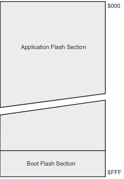
Figure 7. Program Memory Map
$000
$FFF Application Flash Section
SRAM Data Memory
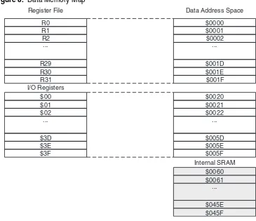
Figure 8 shows how the ATmega8 SRAM Memory is organized.The lower 1120 Data memory locations address the Register File, the I/O Memory, and the internal data SRAM. The first 96 locations address the Register File and I/O Mem-ory, and the next 1024 locations address the internal data SRAM.
The five different addressing modes for the Data memory cover: Direct, Indirect with Displacement, Indirect, Indirect with Pre-decrement, and Indirect with Post-increment. In the Register File, registers R26 to R31 feature the indirect addressing pointer registers.
The direct addressing reaches the entire data space.
The Indirect with Displacement mode reaches 63 address locations from the base address given by the Y- or Z-register.
When using register indirect addressing modes with automatic pre-decrement and post-increment, the address registers X, Y and Z are decremented or incremented.
[image:46.612.197.562.305.620.2]The 32 general purpose working registers, 64 I/O Registers, and the 1024 bytes of inter-nal data SRAM in the ATmega8 are all accessible through all these addressing modes. The Register File is described in “General Purpose Register File” on page 12.
Figure 8. Data Memory Map
Register File
R0 R1 R2
R29 R30 R31 I/O Registers
$00 $01 $02 ...
$3D $3E $3F ...
$0000 $0001 $0002
$001D $001E $001F
$0020 $0021 $0022
...
$005D $005E $005F
...
Data Address Space
$0060 $0061
Data Memory Access
Times
This section describes the general access timing concepts for internal memory access. The internal data SRAM access is performed in two clkCPU cycles as described in Figure 9.
Figure 9. On-chip Data SRAM Access Cycles
EEPROM Data Memory
The ATmega8 contains 512 bytes of data EEPROM memory. It is organized as a sepa-rate data space, in which single bytes can be read and written. The EEPROM has an endurance of at least 100,000 write/erase cycles. The access between the EEPROM and the CPU is described bellow, specifying the EEPROM Address Registers, the EEPROM Data Register, and the EEPROM Control Register.“Memory Programming” on page 222 contains a detailed description on EEPROM Pro-gramming in SPI- or Parallel ProPro-gramming mode.
EEPROM Read/Write Access The EEPROM Access Registers are accessible in the I/O space.
The write access time for the EEPROM is given in Table 1 on page 21. A self-timing function, however, lets the user software detect when the next byte can be written. If the user code contains instructions that write the EEPROM, some precautions must be taken. In heavily filtered power supplies, VCC is likely to rise or fall slowly on Power-up/down. This causes the device for some period of time to run at a voltage lower than specified as minimum for the clock frequency used. See “Preventing EEPROM Corrup-tion” on page 23. for details on how to avoid problems in these situations.
In order to prevent unintentional EEPROM writes, a specific write procedure must be fol-lowed. Refer to the description of the EEPROM Control Register for details on this.
When the EEPROM is read, the CPU is halted for four clock cycles before the next instruction is executed. When the EEPROM is written, the CPU is halted for two clock cycles before the next instruction is executed.
clk
WR
RD Data
Data
Address Address Valid
T1 T2 T3
Compute Address
Read
Wr
ite
CPU
The EEPROM Address
Register – EEARH and EEARL
• Bits 15..9 – Res: Reserved Bits
These bits are reserved bits in the ATmega8 and will always read as zero. • Bits 8..0 – EEAR8..0: EEPROM Address
The EEPROM Address Registers – EEARH and EEARL – specify the EEPROM address in the 512 bytes EEPROM space. The EEPROM data bytes are addressed lin-early between 0 and 511. The initial value of EEAR is undefined. A proper value must be written before the EEPROM may be accessed.
The EEPROM Data Register – EEDR
• Bits 7..0 – EEDR7..0: EEPROM Data
For the EEPROM write operation, the EEDR Register contains the data to be written to the EEPROM in the address given by the EEAR Register. For the EEPROM read oper-ation, the EEDR contains the data read out from the EEPROM at the address given by EEAR.
The EEPROM Control Register – EECR
• Bits 7..4 – Res: Reserved Bits
These bits are reserved bits in the ATmega8 and will always read as zero. • Bit 3 – EERIE: EEPROM Ready Interrupt Enable
Writing EERIE to one enables the EEPROM Ready Interrupt if the I bit in SREG is set. Writing EERIE to zero disables the interrupt. The EEPROM Ready interrupt generates a constant interrupt when EEWE is cleared.
• Bit 2 – EEMWE: EEPROM Master Write Enable
Bit 15 14 13 12 11 10 9 8
– – – – – – – EEAR8 EEARH EEAR7 EEAR6 EEAR5 EEAR4 EEAR3 EEAR2 EEAR1 EEAR0 EEARL
7 6 5 4 3 2 1 0
Read/Write R R R R R R R R/W
R/W R/W R/W R/W R/W R/W R/W R/W
Initial Value 0 0 0 0 0 0 0 X
X X X X X X X X
Bit 7 6 5 4 3 2 1 0
MSB LSB EEDR
Read/Write R/W R/W R/W R/W R/W R/W R/W R/W
Initial Value 0 0 0 0 0 0 0 0
Bit 7 6 5 4 3 2 1 0
– – – – EERIE EEMWE EEWE EERE EECR
Read/Write R R R R R/W R/W R/W R/W
value into the EEPROM. The EEMWE bit must be written to one before a logical one is written to EEWE, otherwise no EEPROM write takes place. The following procedure should be followed when writing the EEPROM (the order of steps 3 and 4 is not essential):
1. Wait until EEWE becomes zero.
2. Wait until SPMEN in SPMCR becomes zero. 3. Write new EEPROM address to EEAR (optional). 4. Write new EEPROM data to EEDR (optional).
5. Write a logical one to the EEMWE bit while writing a zero to EEWE in EECR. 6. Within four clock cycles after setting EEMWE, write a logical one to EEWE.
The EEPROM can not be programmed during a CPU write to the Flash memory. The software must check that the Flash programming is completed before initiating a new EEPROM write. Step 2 is only relevant if the software contains a boot loader allowing the CPU to program the Flash. If the Flash is never being updated by the CPU, step 2 can be omitted. See “Boot Loader Support – Read-While-Write Self-Programming” on page 209 for details about boot programming.
Caution: An interrupt between step 5 and step 6 will make the write cycle fail, since the EEPROM Master Write Enable will time-out. If an interrupt routine accessing the EEPROM is interrupting another EEPROM access, the EEAR or EEDR Register will be modified, causing the interrupted EEPROM access to fail. It is recommended to have the Global Interrupt Flag cleared during all the steps to avoid these problems.
When the write access time has elapsed, the EEWE bit is cleared by hardware. The user software can poll this bit and wait for a zero before writing the next byte. When EEWE has been set, the CPU is halted for two cycles before the next instruction is executed.
• Bit 0 – EERE: EEPROM Read Enable
The EEPROM Read Enable Signal EERE is the read strobe to the EEPROM. When the correct address is set up in the EEAR Register, the EERE bit must be written to a logic one to trigger the EEPROM read. The EEPROM read access takes one instruction, and the requested data is available immediately. When the EEPROM is read, the CPU is halted for four cycles before the next instruction is executed.
The user should poll the EEWE bit before starting the read operation. If a write operation is in progress, it is neither possible to read the EEPROM, nor to change the EEAR Register.
The calibrated Oscillator is used to time the EEPROM accesses. Table 1 lists the typical programming time for EEPROM access from the CPU.
Note: 1. Uses 1 MHz clock, independent of CKSEL Fuse settings.
Table 1. EEPROM Programming Time
Symbol
Number of Calibrated RC
Oscillator Cycles(1) Typ Programming Time
The following code examples show one assembly and one C function for writing to the EEPROM. The examples assume that interrupts are controlled (for example by dis-abling interrupts globally) so that no interrupts will occur during execution of these functions. The examples also assume that no Flash boot loader is present in the soft-ware. If such code is present, the EEPROM write function must also wait for any ongoing SPM command to finish.
Assembly Code Example
EEPROM_write:
; Wait for completion of previous write
sbic EECR,EEWE
rjmp EEPROM_write
; Set up address (r18:r17) in address register
out EEARH, r18
out EEARL, r17
; Write data (r16) to data register
out EEDR,r16
; Write logical one to EEMWE
sbi EECR,EEMWE
; Start eeprom write by setting EEWE
sbi EECR,EEWE
ret
C Code Example
void EEPROM_write(unsigned int uiAddress, unsigned char ucData)
{
/* Wait for completion of previous write */ while(EECR & (1<<EEWE))
;
/* Set up address and data registers */ EEAR = uiAddress;
EEDR = ucData;
/* Write logical one to EEMWE */ EECR |= (1<<EEMWE);
/* Start eeprom write by setting EEWE */
The next code examples show assembly and C functions for reading the EEPROM. The examples assume that interrupts are controlled so that no interrupts will occur during execution of these functions.
EEPROM Write during Power-down Sleep Mode
When entering Power-down sleep mode while an EEPROM write operation is active, the EEPROM write operation will continue, and will complete before the Write Access time has passed. However, when the write operation is completed, the Oscillator continues running, and as a consequence, the device does not enter Power-down entirely. It is therefore recommended to verify that the EEPROM write operation is completed before entering Power-down.
Preventing EEPROM Corruption
During periods of low VCC, the EEPROM data can be corrupted because the supply volt-age is too low for the CPU and the EEPROM to operate properly. These issues are the same as for board level systems using EEPROM, and the same design solutions should be applied.
An EEPROM data corruption can be caused by two situations when the voltage is too low. First, a regular write sequence to the EEPROM requires a minimum voltage to operate correctly. Second, the CPU itself can execute instructions incorrectly, if the sup-ply voltage is too low.
E E P R O M d a t a c o r r u p t i o n c a n e a s i l y b e a v o i d e d b y f o l l o w i n g t h i s d e s i g n recommendation:
Assembly Code Example
EEPROM_read:
; Wait for completion of previous write
sbic EECR,EEWE
rjmp EEPROM_read
; Set up address (r18:r17) in address register
out EEARH, r18
out EEARL, r17
; Start eeprom read by writing EERE
sbi EECR,EERE
; Read data from data register
in r16,EEDR
ret
C Code Example
unsigned char EEPROM_read(unsigned int uiAddress)
{
/* Wait for completion of previous write */
while(EECR & (1<<EEWE)) ;
/* Set up address register */ EEAR = uiAddress;
/* Start eeprom read by writing EERE */ EECR |= (1<<EERE);
/* Return data from data register */
Keep the AVR RESET active (low) during periods of insufficient power supply volt-age. This can be done by enabling the internal Brown-out Detector (BOD). If the detection level of the internal BOD does not match the needed detection level, an external low VCC Reset Protection circuit can be used. If a reset occurs while a write operation is in progress, the write operation will be completed provided that the power supply voltage is sufficient.
I/O Memory
The I/O space definition of the ATmega8 is shown in “” on page 287.All ATmega8 I/Os and peripherals are placed in the I/O space. The I/O locations are accessed by the IN and OUT instructions, transferring data between the 32 general purpose working registers and the I/O space. I/O Registers within the address range 0x00 -0x1F are directly bit-accessible using the SBI and CBI instructions. In these registers, the value of single bits can be checked by using the SBIS and SBIC instructions. Refer to the instruction set section for more details. When using the I/O specific commands IN and OUT, the I/O addresses 0x00 - 0x3F must be used. When addressing I/O Registers as data space using LD and ST instructions, 0x20 must be added to these addresses.
For compatibility with future devices, reserved bits should be written to zero if accessed. Reserved I/O memory addresses should never be written.
Some of the Status Flags are cleared by writing a logical one to them. Note that the CBI and SBI instructions will operate on all bits in the I/O Register, writing a one back into any flag read as set, thus clearing the flag. The CBI and SBI instructions work with reg-isters 0x00 to 0x1F only.
System Clock and
Clock Options
Clock Systems and their
Distribution
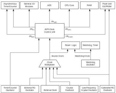
Figure 10 presents the principal clock systems in the AVR and their distribution. All of the clocks need not be active at a given time. In order to reduce power consumption, the clocks to modules not being used can be halted by using different sleep modes, as described in “Power Management and Sleep Modes” on page 33. The clock systems are detailed Figure 10.
Figure 10. Clock Distribution
CPU Clock – clkCPU The CPU clock is routed to parts of the system concerned with operation of the AVR core. Examples of such modules are the General Purpose Register File, the Status Reg-ister and the Data memory holding the Stack Pointer. Halting the CPU clock inhibits the core from performing general operations and calculations.
I/O Clock – clkI/O The I/O clock is used by the majority of the I/O modules, like Timer/Counters, SPI, and USART. The I/O clock is also used by the External Interrupt module, but note that some external interrupts are detected by asynchronous logic, allowing such interrupts to be detected even if the I/O clock is halted. Also note that address recognition in the TWI module is carried out asynchronously when clkI/O is halted, enabling TWI address recep-tion in all sleep modes.
Flash Clock – clkFLASH The Flash clock controls operation of the Flash interface. The Flash clock is usually active simultaneously with the CPU clock.
General I/O Modules Asynchronous
Timer/Counter ADC CPU Core RAM
clkI/O
clkASY
AVR Clock Control Unit
clkCPU
Flash and EEPROM
clkFLASH clkADC
Source Clock
Watchdog Timer
Watchdog Oscillator Reset Logic
Clock Multiplexer
Watchdog Clock
Calibrated RC Oscillator Timer/Counter
Oscillator
Crystal Oscillator
Low-Frequency Crystal Oscillator External RC
[image:53.612.189.576.205.515.2]Asynchronous Timer Clock – clkASY
The Asynchronous Timer clock allows the Asynchronous Timer/Counter to be clocked directly from an external 32 kHz clock crystal. The dedicated clock domain allows using this Timer/Counter as a real-time counter even when the device is in sleep mode. The Asynchronous Timer/Counter uses the same XTAL pins as the CPU main clock but requires a CPU main clock frequency of more than four times the Oscillator frequency. Thus, asynchronous operation is only available while the chip is clocked on the Internal Oscillator.
ADC Clock – clkADC The ADC is provided with a dedicated clock domain. This allows halting the CPU and I/O clocks in order to reduce noise generated by digital circuitry. This gives more accu-rate ADC conversion results.
Clock Sources
The device has the following clock source options, selectable by Flash Fuse Bits as shown below. The clock from the selected source is input to the AVR clock generator, and routed to the appropriate modules.Note: 1. For all fuses “1” means unprogrammed while “0” means programmed.
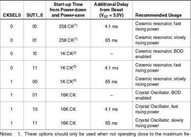
The various choices for each clocking option is given in the following sections. When the CPU wakes up from Power-down or Power-save, the selected clock source is used to time the start-up, ensuring stable Oscillator operation before instruction execution starts. When the CPU starts from reset, there is as an additional delay allowing the power to reach a stable level before commencing normal operation. The Watchdog Oscillator is used for timing this real-time part of the start-up time. The number of WDT Oscillator cycles used for each time-out is shown in Table 3. The frequency of the Watchdog Oscil-lator is voltage dependent as shown in “ATmega8 Typical Characteristics”. The device is shipped with CKSEL = “0001” and SUT = “10” (1 MHz Internal RC Oscillator, slowly ris-ing power).
Table 2. Device Clocking Options Select(1)
Device Clocking Option CKSEL3..0
External Crystal/Ceramic Resonator 1111