FUZZY LOGIC BASED CONTROLLER FOR BUCK CONVERTER
Habibullah1, Irma Husnaini2 and Asnil3
1,2,3 Fakultas Teknik, Universitas Negeri Padang, Padang
ABSTRACT: This research aims to make buck converter prototype for PLTS system by using fuzzy logic controller. Buck converter is required in the PLTS system if the required unidirectional voltage is smaller than the output voltage of the solar cell. Buck converter used to convert 24 Volt dc voltage to 12 Volt dc with 60 watt capability. While fuzzy logic controller is used to improve buck converter performance based on pulse generation technique for switching. The application of fuzzy logic method is expected to improve the performance of the system by maintaining the stability of buck converter output voltage of 12 volts and reduce the output ripple value. Atmega8535 microcontroller is used to generate PWM pulses for switching on power circuits.
Keywords: Buck converter, fuzzy logic, Atmega8535
1. INTRODUCTION
The solar cell is a semiconductor diode that can convert light into electricity and is a major component in a Solar Power System (PLTS). Electrical energy generated by the PLTS in the form of direct current while the load used by consumers can be alternating and direct current. To convert electrical energy from direct current to alternating current an inverter is used, whereas for converting direct current to another level of current is used dc-dc converter. If the required directional voltage is greater than the output voltage of the solar cell then used dc-dc converter type step up or also known as a boost converter. if the unidirectional voltage required is smaller than the output voltage of the solar cell then used dc converter type step down or also known as buck.
Configuration buck on PLTS system can be used for charging battery system which later can be used as source of inverter to convert to voltage back and forth. In addition, buck configurations are also widely used as drivers for LED lights for lighting systems. In PLTS systems, some of the most important dynamic performance criteria to consider are the ripple, the output voltage, and the recovery time.
Buck converter that many in the market still have a high enough ripple rate which consequently reduces the efficiency so that the extent of waste of electric energy is still happening. Therefore, this research focuses on the design of Buck converter for PLTS system using Atmega8535 microcontroller as pulse generator for switching by using fuzzy logic method. The advantages of this buck configuration are better efficiency, simpler circuit, ripple at lower output voltage so that the filter or filter needed is relatively small.
2. LITERATURE REVIEW
2.1 Buck converter
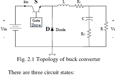
Buck converter shown in Figure 2.1, the output voltage of the buck converter is always lower than the input voltage. Buck converter consists of one active switch (mosfet) and one passive switch (diode). For low working voltage, the passive switch is often replaced by an active switch so that the shrinkage of power that occurs can be reduced. Both of these switches work alternately. At any time there is only one switch that closes. The average value of the converter output voltage is proportional to the ratio between the time of switching of the active switch to its switching period (work factor) [3] [4][5][6]
Fig. 2.1 Topology of buck converter
There are three circuit states: a. Switch S on, Diode D off; b. Switch S off, Diode D on; c. Switch S off, Diode D off.
Switch S is controlled using pulse width modulation (PWM) technique. In this circumstance the sawtooth voltage is compared to the DC voltage. If the sawtooth voltage is lower than the DC voltage then the S switch is closed, otherwise the S switch
S
will open. When the switch is ON, the dynamic current on the inductor IL (t) and the voltage of the capacitor VC (t) can be obtained from the following equation; because the science of modern and methodical fuzzy logic was discovered only a few years ago, when in fact the concept of fuzzy logic itself has been in us for a long time. Fuzzy logic is an appropriate way to map an input space into an output space. The word "Fuzzy" means "vague, vague" and can also mean "fuzzy or impure ideas". Fuzzy logic takes from the second definition, where it starts from an impure idea, then transforms the idea into something pure. This impurity often occurs in a plant system where disturbances from the environment make its variable inputs uncertain. The basic scheme of fuzzy logic can be seen in Figure 2.2. The fuzzy input is a crisp number (declared) expressed in the input set. [8] [9] [10]
Fig. 2.2 The basic scheme of fuzzy
Fuzzy membership functions there are several kinds:
a. Triangle membership function
Fig. 2.3 The set of triangular membership functions
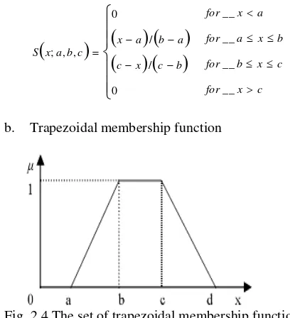
b. Trapezoidal membership function
Fig. 2.4 The set of trapezoidal membership functions
Fuzzy Inference System Knowledge Base
Fuzzyfication Defuzzification
The fuzzy logic control mechanism is shown in Figure 2.5
Fig. 2.5 The mechanism of the closed loop fuzzy logic control calculated using the following equation [1] [10] [11]
)
Fuzzy inference system
Fuzzy inference system is part of the conclusion (reasoning) and decision. Knowledge base contains rules. In general fuzzy rules expressed in the form of 'IF-THEN' which is the essence of fuzzy relation, expressed by R, also called fuzzy implications in basic knowledge can be defined as the set of fuzzy implication phases. If -Then rules consist of two main parts, namely:
a. The antecedent part (premise) is the word between if and then which is the fuzzy input. b. The consequent part (conclusion) is the word
after then which is the fuzzy output.
Thus fuzzy if then rules is the link between the antecedent (fuzzy input) with the corresponding consequent (output fuzzy). So If then rules can be written with:
IF ... (antecedent) THEN ... (Consequent)
The basic rules of fuzzy are in a general form: R: IFx1 is F11 AND ... AND ... Xn is Fn1, THEN
A collection of if-then rules can be made into a table connecting fuzzy input and fuzzy output called Fuzzy Associative Memories (FAM's). The mapping mechanism of fuzzy input to fuzzy output can be mathematically connected with various inference engine methods.
Mamdani Method
In this model the fuzzy rule is defined as: IF x1 is A1 AND ... AND .... Xn is An, THEN y is B
Where A1 ..., An and B are linguistic values (or fuzzy sets) and X1 is A1 states that the variable value of x1 fuzzy member set A1
B2
Fig. 2.6 Inference Engine method of Mamdani model
2.3. Atmega16 Microcontroller
Microcontroller is a programmable IC repeatedly, either written or deleted. Usually used for automatic and manual controls on electronic devices. AVR Atmega 16 microcontroller has a fairly complete feature. ATmega16 AVR microcontroller has been equipped with internal ADC, internal EEPROM, Timer / Counter, PWM, analog comparator, etc. The features possessed by the ATmega16 microcontroller are as follows [12]: a. I / O channels of 32 pieces, namely port A, port
B, port C, and port D. b. Internal ADC of 8 channels.
c. Three Timer / Counter with benchmarking capability.
d. The CPU consists of 32 registers. e. SRAM of 512 bytes.
f. Flash memory of 8 kb with Read Write Write capability.
g. SPI interface port
h. EEPROM of 512 bytes that can be programmed during operation.
i. The analog comparator interface. j. USART port for serial communication.
k. 8-bit microprocessor system based on RISC with a maximum speed of 16 MHz.
Fig. 2.7 Configuration pin ATmega16
From Figure 2.7 can be explained the function of each pin Atmega16 as follows:
a. VCC is a pin that serves as a power supply input.
b. GND embeds the Ground pin.
c. Port A (PortA0 ... PortA7) is a two-way input / output pin and an ADC input pin.
d. Port B (PortB0 ... PortB7) is a two-way input / output pin and and a special function pins Table 1. Special Function of Port B Pin Special function
PB7 SCK (SPI Bus Serial Clock)
PB6 MISO (SPI Bus Master Input/ Slave Output) PB5 MOSI (SPI Bus Master Output/ Slave Input) PB4 SS (SPI Slave Select Input)
PB3 AIN1 (Analog Comparator Negative Input) OC0 (Timer/Counter0 Output Compare Match Output)
PB2 AIN0 (Analog Comparator Positive Input) INT2 (External Interrupt 2 Input)
PB1 T1 (Timer/ Counter1 External Counter Input) PB0 T0 T1 (Timer/Counter External Counter Input)
XCK (USART External Clock Input/Output)
e. Port C (PortC0 ... PortC7) is a two-way input / output pin and a special function pin
Table 2. Special Function of Port C Pin Special function
PC7 TOSC2 ( Timer Oscillator Pin2) PC6 TOSC1 ( Timer Oscillator Pin1) PC5 Input/Output
PC4 Input/Output PC3 Input/Output PC2 Input/Output
PC1 SDA ( Two-wire Serial Buas Data Input/Output Line)
PC0 SCL ( Two-wire Serial Buas Clock Line)
f. Port D (PortD0 ... PortD7) is a two-way input / output pin and a special function pin
Table 3. Special Function of Port D Pin Special function
PD7 OC2 (Timer/Counter Output Compare Match Output)
Pin Fungsi khusus
PD7 OC2 (Timer/Counter Output Compare Match Output)
PD6 ICP (Timer/Counter1 Input Capture Pin) PD5 OC1A (Timer/Counter1 Output Compare A
Match Output)
PD4 OC1B (Timer/Counter1 Output Compare B Match Output)
PD3 INT1 (External Interrupt 1 Input) PD2 INT0 (External Interrupt 0 Input) PD1 TXD (USART Output Pin) PD0 RXD (USART Input Pin)
g. RESET is the pin that is used to reset the microcontroller.
h. XTAL1 and XTAL2 are external clock input pins.
i. AVCC is the input voltage pin for ADC. j. AREFF is the input pin of the ADC reference
voltage
3. RESEARCH METHODS
This research activity is planned to produce a prototype of Buck converter with 60 VA capability. Stages of activities undertaken to conduct this research can be described as follows
Use at most three levels of headings that correspond to chapters, sections and subsections. The first level headings for chapter titles should be in 10pt, bold, justified, and upper case font. Leave one-blank line before and after the first level headings, respectively.
3.1 Buck converter simulation
In the early stages of this research, Buck converter simulation was performed with the intention to get a good performance in accordance with the desired prototype
3.2 Component Selection
The next stage is to select the design components based on simulations that have been done in the early stages. At this stage a list of required components and their specifications will be obtained.
3.3 Purchase of Parts / Equipment
3.4. Assembling
At this stage the assembly is based on the tested development model and the selected components. The results to be achieved at this stage is the assembly of Buck converter prototypes
3.5 Testing
In this stage, the feasibility test of the technical results of the assembly. If the test results do not provide the expected performance, then its required the improvement of the design system. The results to be achieved at this stage is the operation of Buck converter prototypes that can optimize the use of solar energy
3.6 Reporting
At this stage conducted reporting of research results. Reporting of results is made in the form of a report book
4. RESULTS AND DISCUSSION
4.1 Buck Converter Simulation
Before making a prototype buck converter with 60A capability, then first do the design and simulate it. This simulation result is needed to see the characteristics of this type of converter buck
Fig. 4.1 Response system without a controller
Fuzzy logic control uses error e (k) and error
change Δe = e (k) - e (k-1). Errors are defined as the difference between the reference and the output measurement values
Fig. 4.2 Input variable error (e(k))
Fig. 4.3 Input variable delta error (Δe)
Fig. 4.4 Output variable of pwm
Fig. 4.5 Response system with a controller
3.2 Buck Hardware Converter generated
The following figure shows the hardware of the completed buck converter
Fig. 4.6 Buck Converter circuit
Fig. 4.7 Gate Drive circuit
0 0.5 1 1.5 2 2.5
x 10-3
0 2 4 6 8 10 12 14 16 18
Step Response
Time (sec)
V
o
lta
g
e
(
V
)
0 5 10 15 20 25 30 35 40 45 50
Fig. 4.8 Microcontroller circuit
3.3 Buck Converter Testing
Fig. 4.9 Testing circuit Buck Converter
Fig. 4.10 Open loop response output of buck converter without controller
Figure 4.10 shows the slow system response to the steady state state, although there is no ripple, because the load is too small.
Fig. 4.11 Closed loop response output buck converter with controller
Figure 4.11 shows the rapid response of the system to the steady state, although there is a ripple, but it does not result in overshoot. From the picture also seen the output voltage generated is 12.4 VDC.
5. CONCLUSION
The converted buck converter has 24 VDC input with 12 VDC output capability of 60 VA maximum. Testing a buck converter using a 100 Ohm 5 watt load shows a fairly good response with an output voltage of 12.4 VDC.
This Buck Converter circuit can be used for PLTS system with maximum ability of 60 VA
6. REFERENCES
[1] Gopal, M, 2004, Digital Control and State Variable Methods, 2nd Edition, McGraw-Hill
Publishing Company Limited.
[2] Phillips, L. Charles, 1995, Digital control System, 3rd Edition, Prentice Hall International.
Inc.
[3] Kasat, Saurabh. Analysis , Design and Modeling of DC-DC Converter Using Simulink. Bachelor of Engineering Institute of Engineering and Technology Indore, Madhya Pradesh State India. 2004
[4] Husnaini, Irma, Asnil. Perancangan Kompensator PI- Lead Pada Kestabilan Tegangan Buck converter. Jurnal Teknologi Informasi dan Pendidikan. Vol 5 No 2 Maret 2012
[5] Qiao, Michael, Parviz Parto and Reza Amirani.
Stabilize The buck converter with
Transkonduktansi Amplifier. International Rectifier. 2002.
[6] Tymerski, Richard and Frank Rytkonen:
Control System Design
Electrical Engineering, Vol. 7, No. 1,p. 57-68.May 2010.
[8] Jang, J.R, 1997,Neuro Fuzzy and Soft Computing, International Edidtion, Printice Hall.
[9] Passino, Kevin M. Passino and Stephen Yurkovich , 1998, Fuzzy Control, Addison wesley
[10]Behrouz Safarinejadian and Farzaneh Jafartabar. Hybrid Fuzzy Logic Controllers for Buck Converter. International Conference on Artificial Intelligence and Image Processing (ICAIIP'2012) Oct. 6-7, 2012 Dubai (UAE )
[11]U, Bhagyashri Patil 7 Prof. S. R. Jagtap. Design of Fuzzy Based Controlling System for Buck Converter . International Journal of Advanced Research in Computer Engineering & Technology (IJARCET) Volume 4 Issue 6, June 2015