Emerging Silicon and Non-Silicon Nanoelectronic Devices:
Opportunities and Challenges for
Future High-Performance and Low-Power Computational Applications
(Invited Paper)
Robert Chau, Justin Brask, Suman Datta, Gilbert Dewey, Mark Doczy, Brian Doyle, Jack Kavalieros, Ben Jin, Matthew Metz, Amlan Majumdar, and Marko Radosavljevic
Components Research, Logic Technology Development, Intel Corporation, Mail Stop RA3-252, 5200 NE Elam Young Parkway, Hillsboro, OR 97124, USA
Email: [email protected]
A
BSTRACTSeveral key emerging nanoelectronic devices, such as Si nanowire field-effect transistors (FETs), carbon nanotube FETs, and III-V compound semiconductor quantum-well FETs, are assessed for their potential in future high-performance, low-power computation applications. Furthermore, these devices are benchmarked against state-of-the-art Si CMOS technologies. The two fundamental transistor benchmarking metrics utilized in this study are (i) CV/I
versus LG and ii) CV/I versus ION /IOFF. While intrinsic device speed is emphasized in the first metric, the tradeoff between device speed and off-state leakage is assessed in the latter. For high-performance and low-power logic applications, low CV/I and high ION /IOFF values are both required. Based on the results obtained, the opportunities and challenges for these emerging novel devices in future logic applications are highlighted and discussed.
I.
I
NTRODUCTIONAccording to Moore’s Law, the number of transistors per integrated circuit doubles every 24 months, and it has been the guiding principle for the semiconductor industry for over 30 years. The sustaining of Moore’s Law, however, requires continued transistor scaling and performance improvements. The physical gate length LG of the Si transistors used in the 90 nm logic generation node is ~ 50 nm. It is projected that transistor LG will reach ~ 10 nm in 2011. By way of innovation in silicon technology, such as strained-Si channels [1, 2], high-κ/metal-gate stacks [3–5], and the non-planar Tri-gate CMOS transistor architecture [6], CMOS transistor scaling and performance will continue at least until the middle of the next decade. Recently, a lot of interest generated has been generated and good progress has been made in the study of novel silicon and non-silicon nanoelectronic devices, including Si-nanowire field-effect transistors (FETs) [7–11], carbon-nanotube FETs (CNTFETs) [12–18], and III-V compound semiconductor quantum-well FETs (QWFETs) [19, 20], in the capacity of future computation applications. These devices hold promise as candidates for integration with the ubiquitous silicon platform in order to enhance circuit functionality while simultaneously enabling the extension of Moore’s Law well into the next decade and beyond. In this work, two fundamental device metrics, namely (i) CV/I versus
LG and (ii) CV/I versus ION /IOFF, are used to benchmark these emerging nano-electronic devices vis-à-vis state-of-the-art Si CMOS transistors with regard to high-performance, low-power logic CMOS-like applications. These benchmarking metrics and corresponding methodologies have previously been described in great detail [21, 22]. While the first metric highlights the intrinsic
speed of devices, the latter permits an assessment of the tradeoff between device intrinsic speed and off-state leakage. Data from our own research devices and also from literature were used in this study. The merits and potential shortcomings of these emerging devices will be discussed. Figure 1 shows the images of some of the novel research transistors discussed in this work.
II.
E
MERGINGP-C
HANNELN
ANOELECTRONICD
EVICESThe room temperature CV/I versus LG comparison of conventional Si transistors, Si nanowire transistors, and CNT transistors with p-channels is shown in Figure 2. The data indicate that CNTs exhibit significant CV/I improvement when compared to conventional Si devices. This improvement is due primarily to the mobility enhancement in CNTs. By contrast, the CV/I characteristics of Si nanowire devices and conventional Si devices are similar. A recent report suggests that, fundamentally, there is no reason to expect Si nanowire transistors to have higher channel mobility than standard planar Si devices at room temperature [23]. For example, TCAD simulations have shown that phonon scattering increases, and
FIGURE 1. TEM cross-section and SEM images of research transistors. (a) Planar Si MOSFET with physical gate length LG = 10 nm, (b) non-planar Si
hence the phonon-limited mobility decreases, at room temperature for devices containing Si nanowires with diameters less than 15 nm [23]. Additionally, experimental studies reveal that while phonon scattering in Si nanostructures is suppressed at low temperatures, phonon scattering limited transport is indeed prevalent at room temperature, limiting effective channel mobility, as shown in Figure 3. Hence, at room temperature, Si nanowires with dimensions of interest for scaling do not exhibit transistor performance enhancement when compared to conventional planar Si architectures, as shown in Figure 2.
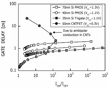
The p-channel CV/I versus ION /IOFF characteristics of the CNT-FET are shown in Figure 4. Included in this figure are data from conventional planar Si and non-planar Tri-gate Si transistors for comparison. Despite the observation that CNTFETs exhibit high intrinsic speed (CV/I) performance, as shown in Figure 2, they in fact suffer from a low ION /IOFF ratio. This low ratio is attributed to a high
IOFF for the CNTFET, as shown in Figure 5, which in turn is due to the existence of ambipolar leakage [15, 21, 22]. The ambipolar leakage is a consequence of metal-CNT Schottky contacts, which are used instead of standard implanted or diffused p-n junctions. It is
anticipated that the use of standard p-n junctions will eliminate ambipolar leakage and improve the ION /IOFF ratios of CNTFETs. It is noted, however, that for high-performance and low-power logic applications, both low CV/I and high ION /IOFF values are required.
III.
E
MERGINGN-C
HANNELN
ANOELECTRONICD
EVICESFigure 6 shows the room temperature CV/I versus LG comparison of conventional Si transistors, CNT transistors, and III-V (InSb) compound semiconductor QW transistors [19, 20] with n-channels. In comparison with conventional Si devices, InSb transistors exhibit significantly larger n-channel intrinsic speed (CV/I), a benefit of higher channel mobility and lower utilized supply voltage VCC (0.5 V). The increased channel mobility also translates to a high-frequency gain in InSb transistors, as shown in Figure 7 [20]. In this case, the dc CV/I data is directly correlated to the ac cutoff-frequency
fT data.
The n-channel CNT devices in Figure 6 all show degraded CV/I
performance compared to conventional Si n-channel devices. This
FIGURE 2.Gate delay (intrinsic device speed) CV/I versus transistor physical gate length LG of PMOS devices. The diameters of the CNTs are within the
1.0-2.5 nm range while those of the Si nanowires are within the 4-35 nm range.
FIGURE 3.Effective electron mobility µeffas a function of effective vertical
field Eeff of a Si nano-fin structure in the temperature range T = 10-290 K.
Note that the T = 10 and 50 K curves overlap each other. The primary scattering mechanisms: phonon scattering, surface-roughness scattering, and Coulomb scattering, are identified on the plot. The impact of phonon scattering becomes significant above 50 K. At effective fields of interest, the effective mobilities at higher temperatures are lower than those at lower temperatures.
FIGURE 4.Gate delay (intrinsic device speed) CV/I versus on-to-off state current ratio ION/IOFF of Si PMOS transistors with physical gate length LG= 70
nm at supply voltage VCC = 1.3 V and LG = 40 nm at VCC = 1.1 V, a Si Trigate
PMOS transistor with LG = 35 nm at VCC = 1.1 V, and a CNT PMOS
transistor with LG = 50 nm at VCC = 0.3 V [17]. The ION /IOFF ratio in
CNTFETs is limited by the ambipolar conduction.
FIGURE 5.ID-VGcharacteristics of a carbon nanotube PMOS transistor with Pd
metal source-drain at different drain biases VDS, illustrating ambipolar
phenomenon can possibly be explained by considering that a suitable n-type workfunction metal that forms a stable interface with CNTs has yet to be demonstrated. Upon resolution of this issue, a high performance n-channel CNTFET is anticipated based on the symmetry of the conduction and valence bands for CNTs [24].
In Figure 8, n-channel CV/I versus ION /IOFF characteristics are shown for CNTFETs with chemically-doped junctions [18] and for InSb QWFETs. Also shown, for the sake of direct comparison, are conventional planar Si and non-planar Tri-gate Si transistors. The use of chemically-doped junctions in CNTFETs [18], as opposed to metal-CNT Schottky junctions, suppresses the ambipolar leakage conduction and reduces IOFF, thus improving the ION /IOFF ratio. However, the resulting CV/I performance is still degraded, possibly due to increased external parasitic resistance of the doped junctions. Nevertheless, this chemically-doped junction approach is indeed a major advancement for CNTFET research [18].
Interestingly, the n-channel InSb QWFET also exhibits a low
ION/IOFF ratio, as shown in Figure 8. This phenomenon is a consequence of high gate leakage, as exhibited in Figure 9, due to the low barrier height at the Schottky metal-semiconductor junction. The low barrier height arises from (a) Fermi-level pinning at the
metal-semiconductor interface and (b) the use of a narrow-bandgap semiconductor. It is predicted that the use of a gate dielectric between the metal gate and the III-V device layers will eliminate such Schottky gate leakages and improve the ION /IOFF ratio [20].
IV.
C
ONCLUSIONSIn this paper, we have identified the merits and potential shortcomings of various emerging nanoelectronic devices with respect to future logic applications. Specifically, we have shown that (a) Si nanowires offer no transistor CV/I performance advantage over conventional Si transistors at room temperature, likely due to the significant role played by phonon scattering at room temperature, and that (b) both p-channel CNTFETs and n-channel QWFETs exhibit impressive CV/I gain when compared against conventional Si transistors, but they suffer from degraded ION/IOFF ratios, a result of ambipolar conduction and Schottky gate leakage, respectively. Based
FIGURE 6.Gate delay (intrinsic device speed) CV/I versus transistor physical gate length LG of NMOS devices. The diameters of the CNTs are within the
1.0-2.5 nm range.
FIGURE 7.Cutoff frequency fT versus dynamic power dissipation of an
n-channel InSb QWFET with gate length LG = 200 nm and a Si NMOS with LG
= 80 nm at different values of drain bias VDS. fT is obtained from
high-frequency measurement of transistor s-parameters [20].
FIGURE 8.Gate delay (intrinsic device speed) CV/I versus on-to-off state current ratio ION /IOFFof Si NMOS transistors with physical gate length LG=
70 nm at supply voltage VCC= 1.3 V and LG= 40 nm at VCC= 1.1 V, a Si
Trigate NMOS transistor with LG = 35 nm at VCC = 1.1 V, an InSb n-type
quantum-well FET (QWFET) with LG= 200 nm at VCC= 0.5 V [20], and a
CNT NMOS transistor with LG = 80 nm at VCC = 0.5 V [18]. The use of
chemically-doped junctions [18] delays the ambipolar conduction in the CNTFET, despite poor gate delay performance. Nevertheless, this represents a major breakthrough in CNTFET research [18]. The ION /IOFFratio of the
InSb QWFET is limited by Schottky gate leakage [20].
FIGURE 9.Drain current IDS and gate leakage current IGversus gate voltage VGSof an InSb n-type quantum-well FET (QWFET) with physical gate length LG = 200 nm. Inset: Schematic of device layers in III-V material-based
QWFETs with Schottky metal gates. IG is the Schottky gate leakage due to
on this study, we anticipate that upon solving the off-state leakage problems, high-mobility devices such as CNTFETs and III-V QWFETs have the potential to enable high-performance logic applications with very low supply voltage VCC (e.g. below 0.5 V).
R
EFERENCES[1] S. E. Thompson, M. Armstrong, C. Auth, S. Cea, R. Chau, G. Glass, T. Hoffman, J. Klaus, Z. Ma, B. McIntyre, A. Murthy, B. Obradovic, L. Shifren, S. Sivakumar, S. Tyagi, T. Ghani, K. Mistry, M. Bohr, and Y. El-Mansy, “A logic nanotechnology featuring strained-silicon”, IEEE Electron Device Letters, vol. 25, pp. 191–193, 2004.
[2] S. Datta, G. Dewey, M. Doczy, B. S. Doyle, B. Jin, J. Kavalieros, R. Kotlyar, M. Metz, N. Zelick, and R. Chau, “High mobility Si/SiGe strained channel MOS transistors with HfO2/TiN gate stack”, IEDM Technical Digest, pp. 653–656,
2003.
[3] R. Chau, S. Datta, M. Doczy, J. Kavalieros, and M. Metz, “Gate dielectric scaling for high-performance CMOS: from SiO2 to
high-κ”, Extended Abstract of International Workshop on Gate Insulator, Tokyo, Japan, pp. 124–126, 2003.
[4] R. Chau, “Advanced metal gate/high-κ dielectric stacks for high-performance CMOS transistors”, AVS 5th International
Conference on Microelectronics and Interfaces, Santa Clara, CA, USA, pp. 3–5, 2004.
[5] R. Chau, S. Datta, M. Doczy, B. Doyle, J. Kavalieros, and M. Metz, “High-κ/metal-gate stack and its MOSFET characteristics”, IEEE Electron Device Letters, vol. 25, pp. 408– 409, 2004.
[6] R. Chau, B. Doyle, J. Kavalieros, D. Barlage, A. Murthy, M. Doczy, R. Arghavani, and S. Datta, “Advanced depleted-substrate transistors: single-gate, double-gate and tri-Gate”,
Extended Abstracts of International Conference on Solid State Devices and Materials, Nagoya, Japan, pp. 68-69, 2002. [7] Y. Cui, X. Duan, J. Hu, and C. M. Lieber, “Doping and
electrical transport in silicon nanowires”, Journal of Physical Chemistry B, vol. 104, pp. 5213–5216, 2000.
[8] L. J. Lauhon, M. S. Gudiksen, D. Wang, and C. M. Lieber, “Epitaxial core-shell and core-multishell nanowire heterostructures”, Nature, vol. 420, pp. 57–61, 2002.
[9] Y. Cui, Z. Zhong, D. Wang, W. U. Wang, and C. M. Lieber, “High performance silicon nanowire field effect transistors”,
Nano Letters, vol. 3, p. 149–152, 2003.
[10]M. C. McAlpine, R. S. Friedman, S. Jin, K. Lin, W. U. Wang, and C. M. Lieber, “High-performance nanowire electronic and photonics on glass and plastic substrates”, Nano Letters, vol. 3, pp. 1531–1535, 2003.
[11]S. Jin, D. Whang, M. C. McAlpine, R. S. Friedman, Y. Wu, and C. M. Lieber, “Scalable interconnection and integration of nanowire devices without registration”, Nano Letters, vol. 4, pp. 915–919, 2004.
[12]A. Javey, H. Kim, M. Brink, Q. Wang, A. Ural, J. Guo, P. McIntyre, P. McEuen, M. Lundstrom, and H. Dai, “High-κ dielectrics for advanced carbon nanotube transistors and logic gates”, Nature Materials, vol. 1, pp. 241–246, 2002.
[13]S. J. Wind, J. Appenzeller, R. Martel, V. Derycke, and Ph. Avouris, “Vertical scaling of carbon nanotube field-effect transistors using top gate electrodes”, Applied Physics Letters, vol. 80, pp. 3817–3819, 2002.
[14]S. Rosenblatt, Y. Yaish, J. Park, J. Gore, V. Sazonova, and P. L. McEuen, “High performance electrolyte gated carbon nanotube transistors”, Nano Letters, vol. 2, pp. 869–872, 2002. [15]M. Radosavljevic, S. Heinze, J. Tersoff, and Ph. Avouris,
“Drain voltage scaling in carbon nanotube transistors”, Applied Physics Letters, vol. 83, pp. 2435–2437, 2003.
[16]A. Javey, J. Guo, D. B. Farmer, Q. Wang, D. Wang, R. G. Gordon, M. Lundstrom, and H. Dai, “Carbon nanotube field-effect transistors with integrated ohmic contacts and high-κ gate dielectrics”, Nano Letters, vol. 4, pp. 447–450, 2004.
[17]A. Javey, J. Guo, D. B. Farmer, Q. Wang, E. Yenilmez, R. G. Gordon, M. Lundstrom, and H. Dai, “Self-aligned ballistic molecular transistors and electrically parallel nanotube arrays”,
Nano Letters, vol. 4, pp. 1319–1322, 2004.
[18]A. Javey, R. Tu, D. B. Farmer, J. Guo, R. G. Gordon, and H. Dai, “High performance n-type carbon nanotube field-effect transistors with chemically doped contacts”, Nano Letters, vol. 5, pp. 345–348, 2005.
[19]T. Ashley, A. B. Dean, C. T. Elliott, R. Jefferies, F. Khaleque, and T. J. Phillips, “High-speed low-power InSb transistors”,
IEDM Technical Digest, pp. 751–754, 1997.
[20]T. Ashley, A. Barnes, L. Buckle, S. Datta, A. Dean, M. Emeny, M. Fearn, D. Hayes, K. Hilton, R. Jefferies, T. Martin, K. Nash, T. Philips, W. Tang, P. Wilding, and R. Chau, “Novel InSb-based quantum well transistors for ultra-high speed, low power logic applications”, Proceedings of 7th International Conference
on Solid-State and Integrated Circuits Technology, Beijing, China, pp. 2253-2256, 2004.
[21]R. Chau, “Benchmarking nanotechnology for high-performance and low-power logic transistor applications”, Proceedings of 4th
IEEE Conference on Nanotechnology, Munich, Germany, 2004. [22]R. Chau S. Datta, M. Doczy, B. Doyle, B. Jin, J. Kavalieros, A.
Majumdar, M. Metz, and M. Radosavljevic, “Benchmarking nanotechnology for high-performance and low-power logic transistor applications”, IEEE Transactions on Nanotechnology, vol. 4, March 2005.
[23]R. Kotlyar, B. Obradovic, P. Matagne, M. Stettler, and M. D. Giles, “Assessment of room-temperature phonon-limited mobility in gated silicon nanowires”, Applied Physics Letters, vol. 84, pp. 5270–5272, 2004.