II
Architecture and
Organization
Computer architecture is the design and organization of efficient and effective computer hardware at all levels — from the most fundamental aspects of logic and circuit design to the broadest concerns of RISC, parallel, and high-performance computing. Individual chapters cover the design of the CPU, memory systems, buses, disk storage, and computer arithmetic devices. Other chapters treat important subjects such as parallel architectures, the interaction between computers and networks, and the design of computers that tolerate unanticipated interruptions and failures.
16 Digital Logic Miriam Leeser
Introduction • Overview of Logic • Concept and Realization of a Digital Gate
• Rules and Objectives in Combinational Design • Frequently Used Digital Components • Sequential Circuits • ASICs and FPGAs — Faster, Cheaper, More Reliable Logic 17 Digital Computer Architecture David R. Kaeli
Introduction • The Instruction Set • Memory • Addressing • Instruction Execution • Execution Hazards • Superscalar Design • Very Long Instruction Word
Computers • Summary
18 Memory Systems Douglas C. Burger, James R. Goodman, and Gurindar S. Sohi Introduction • Memory Hierarchies • Cache Memories • Parallel and Interleaved
Main Memories • Virtual Memory • Research Issues • Summary
19 Buses Windsor W. Hsu and Jih-Kwon Peir
Introduction • Bus Physics • Bus Arbitration • Bus Protocol • Issues in SMP System
Buses • Putting It All Together --- CCL-XMP System Bus • Historical Perspective and
Research Issues
20 Input/Output Devices and Interaction Techniques Ken Hinckley, Robert J. K. Jacob, and Colin Ware
Introduction • Interaction Tasks, Techniques, and Devices • The Composition of
Interaction Tasks • Properties of Input Devices • Discussion of Common Pointing
Devices • Feedback and Perception — Action Coupling • Keyboards, Text Entry, and
Command Input • Modalities of Interaction • Displays and Perception • Color Vision
and Color Displays • Luminance, Color Specification, and Color Gamut • Information
Visualization • Scale in Displays • Force and Tactile Displays • Auditory
Displays • Future Directions
21 Secondary Storage Systems Alexander Thomasian
Introduction • Single Disk Organization and Performance • RAID Disk Arrays • RAID1 or Mirrored Disks • RAID5 Disk Arrays • Performance Evaluation
22 High-Speed Computer Arithmetic Earl E. Swartzlander Jr. Introduction • Fixed Point Number Systems • Fixed Point Arithmetic
Algorithms • Floating Point Arithmetic • Conclusion
23 Parallel Architectures Michael J. Flynn and Kevin W. Rudd Introduction • The Stream Model • SISD • SIMD • MISD • MIMD • Network Interconnections • Afterword
24 Architecture and Networks Robert S. Roos
Introduction • Underlying Principles • Best Practices: Physical Layer Examples • Best Practices: Data-Link Layer Examples • Best Practices: Network Layer
Examples • Research Issues and Summary
25 Fault Tolerance Edward J. McCluskey and Subhasish Mitra
Introduction • Failures, Errors, and Faults • Metrics and Evaluation • System Failure
Response • System Recovery • Repair Techniques • Common-Mode Failures and Design
16
Digital Logic
Miriam Leeser Northeastern University
16.1 Introduction 16.2 Overview of Logic
16.3 Concept and Realization of a Digital Gate
CMOS Binary Logic Is Low Power • CMOS Switching Model for NOT, NAND, and NOR •Multiple Inputs and Our Basic Primitives• Doing It All with NAND
16.4 Rules and Objectives in Combinational Design
Boolean Realization: Half Adders, Full Adders, and Logic Minimization • Axioms and Theorems of Boolean Logic •Design, Gate-Count Reduction, and SOP/POS Conversions
•Minimizing with Don’t Cares •Adder/Subtractor
•Representing Negative Binary Numbers
16.5 Frequently Used Digital Components
Elementary Digital Devices: ENC, DEC, MUX, DEMUX •The Calculator Arithmetic and Logical Unit
16.6 Sequential Circuits
Concept of a Sequential Device• The Data Flip-Flop and the Register• From DFF to Data Register,
Shift Register, and Stack• Datapath for a 4-bit Calculator
16.7 ASICs and FPGAs --- Faster, Cheaper, More Reliable Logic
FPGA Architecture • Higher Levels of Complexity
16.1 Introduction
zero one
0 volts (v) .8v 1.7v 2.5v
FIGURE 16.1 The states zero and one as defined in 2.5V CMOS logic.
16.2 Overview of Logic
Logic has been a favorite academic subject, certainly since the Middle Ages and arguably since the days of the greatness of Athens. That use oflogicconnoted the pursuit of orderly methods for defining theorems and proving their consistency with certain accepted propositions. In the middle of the 19th century, George Boole put the whole subject on a sound mathematical basis and spread “logic” from the Philosophy Department into Engineering and Mathematics. (Boole’s original writings have recently been reissued [Boole 1998].) Specifically, what Boole did was to create an algebra of two-valued (binary) variables. Initially designated astrueorfalse, these two values can represent any parameter that has two clearly defined states. Boolean algebras of more than two values have been explored, but the original binary variable of Boole dominates the design of circuitry for reasons that we will explore. This chapter presents some of the rules and methods of binary Boolean algebra and shows how it is used to design digital hardware to meet specific engineering applications.
One of the first things that must strike a reader who seestrueorfalseproposed as the two identifiable, discrete states is that we live in a world with many half-truths, with hung juries that end somewhere betweenguiltyandnot guilty, and with “not bad” being a response that does not necessarily mean “good.” The answer to the question: “Does a two-state variable really describe anything?” is properly: “Yes and no.” This apparent conflict between the continuum that appears to represent life and the underlying reality of atomic physics, which is inherently and absolutely discrete, never quite goes away at any level. We use the words “quantum leap” to describe a transition between two states with no apparent state between them. Yet we know that the leaper spends some time between the two states.
A system that is well adapted to digital (discrete) representation is one that spends little time in a state of ambiguity. All digital systems spend some time in indeterminate states. One very common definition of the two states is made for systems operating between 2.5 volts (V) and ground. It is shown in Figure 16.1. One state, usually calledone, is defined as any voltage greater than 1.7V. The other state, usually called zero, is defined as any voltage less than 0.8V.
The gray area in the middle isambiguous. When an input signal is between 0.8 and 1.7V in a 2.5V CMOS (complementary metal–oxide–semiconductor) digital circuit, you cannot predict the output value. Most of what you will read in this chapter assumes that input variables are clearly assigned to the stateoneor the statezero. In real designs, there are always moments when the inputs are ambiguous. A good design is one in which the system never makes decisions based on ambiguous data. Such requirements limit the speed of response of real systems; they must wait for the ambiguities to settle out.
16.3 Concept and Realization of a Digital Gate
Agateis the basic building block of digital circuits. A gate is a circuit with one or more inputs and a single output. From a logical perspective in a binary system, any input or output can take on only the valuesone andzero. From an analog perspective (a perspective that will vanish for most of this chapter), the gates make transitions through the ambiguous region with great rapidity and quickly achieve an unambiguous state ofonenessorzeroness.
TABLE 16.1 The Boolean Operators of Two Input Variables
TABLE 16.2 The Boolean Operators Extended to More than Two Inputs
Operation Input Variables Operator Symbol Output = 1 if
NOT A A A=0
FIGURE 16.2 Commonly used graphical symbols for seven of the gates defined in Table 16.1.
“inclusive or” function because it includes the case whereAandBare both true. There is another Boolean operator,exclusive or, that is true when eitherAorB, but not both, is true. In fact, there are 16 Boolean functions of two variables. The more useful functions are shown in truth table form in Table 16.1. These functions can be generalized to more than one variable, as is shown in Table 16.2.
AND, OR, and NOT are sufficient to describe all Boolean logic functions. Why do we need all these other operators?
Logic gates are themselves an abstraction. The actual physical realization of logic gates is with tran-sistors. Most digital designs are implemented in CMOS technology. In CMOS and most other transistor technologies, logic gates are naturally inverting. In other words, it is very natural to build NOT, NAND, and NOR gates, even if it is more natural to think about positive logic: AND and OR. Neither XOR nor XNOR are natural building blocks of CMOS technology. They are included for completeness. AND and OR gates are implemented with NAND and NOR gates as we shall see.
One question that arises is: How many different gates do we really need? The answer is one. We normally admit three or four to our algebra, but one is sufficient. If we pick the right gate, we can build all the others. Later we will explore the minimal set.
B
C D A
AB + CD
B A
A XOR B
FIGURE 16.3 Two constructs built from the gates in column 1 ofFigure 16.2.The first is a common construct in which if either of two paired propositions is TRUE, the output is TRUE. The second is XOR constructed from the more primitive gates, AND, OR, and NOT.
circle). Often, the inversion operation alone is used, as seen in the outputs of NAND, NOR, and XNOR. In writing Boolean operations we use the symbolsAfor NOT A,A+Bfor A OR B, andA·Bfor A AND B. A+Bis called the sum ofAandBandA·Bis called the product. The operator for AND is often omitted, and the operation is implied by adjacency, just like in multiplication. To illustrate the use of these symbols and operators and to see how well these definitions fit common speech, Figure 16.3 shows two constructs made from the gates of Figure 16.2. These two examples show how to build the expressionAB+C Dand how to construct an XOR from the basic gates AND, OR, and NOT.
The first construct of Figure 16.3 would fit the logic of the sentence: “I will be content if my federal and state taxes are lowered (Aand B, respectively), or if the money that I send is spent on reasonable things and spent effectively (CandD, respectively).” You would certainly expect the speaker to be content if either pair is TRUE and most definitely content if both are TRUE. The output on the right side of the construct is TRUE if either or both of the inputs to the OR is TRUE. The outputs of the AND gates are TRUE when both of their inputs are TRUE. In other words, both state and federal taxes must be reduced to make the top AND’s output TRUE.
The right construct in Figure 16.3 gives an example of how one can build one of the basic logic gates, in this case the XOR gate, from several of the others. Let us consider the relationship of this construct to common speech. The sentence: “With the time remaining, we should eat dinner or go to a movie.” The implication is that one cannot do both. The circuit on the right of Figure 16.3 would indicate an acceptable decision (TRUE if acceptable) if either movie or dinner were selected (assertedor made TRUE) but an unacceptable decision if both or neither were asserted.
What makes logic gates so very useful is their speed and remarkably low cost. On-chip logic gates today can respond in less than a nanosecond and can cost less than 0.0001 cent each. Furthermore, a rather sophisticated decision-making apparatus can be designed by combining many simple-minded binary decisions. The fact that it takes many gates to build a useful apparatus leads us back directly to one of the reasons why binary logic is so popular. First we will look at the underlying technology of logic gates. Then we will use them to build some useful circuits.
16.3.1 CMOS Binary Logic Is Low Power
A modern microcomputer chip contains more than 10 million logic gates. If all of those gates were generating heat at all times, the chip would melt. Keeping them cool is one of the most critical issues in computer design. Good thermal designs were significant parts of the success of Cray, IBM, Intel, and Sun. One of the principal advantages of CMOS binary logic is that it can be made to expend much less energy to generate the same amount of calculation as other forms of circuitry.
gate. When you start with more than 1 million gates per chip, small reductions in power dissipation make the difference between usable and unusable chips.
Saturated logic issaturatedbecause it is driven hard enough to ensure that it is in a minimum-dissipation state. Because it takes some effort to bring such logic out of saturation, it is a little slower than active logic. Active logic, on the other hand, is always dissipative. It is very fast, but it is always getting hot. Although it has often been the choice for the most active circuits in the fastest computers, active logic has never been a major player, and it owns a diminishing role in today’s designs. This chapter focuses on today’s dominant family of binary, saturated logic, which is CMOS: Complementary Metal Oxide Semiconductor.
16.3.2 CMOS Switching Model for NOT, NAND, and NOR
The metal–oxide–semiconductor (MOS) transistor is the oldest transistor in concept and still the best in one particular aspect: its control electrode — also called agatebut in a different meaning of that word fromlogic gate— is a purely capacitive load. Holding it at constant voltage takes no energy whatsoever. These MOS transistors, like most transistors, come in two types. One turns on with a positive voltage; the other turns off with a positive voltage. This pairing allows one to buildcomplementarygates, which have the property that they dissipate no energy except when switching. Given the large number of logic gates and the criticality of energy dissipation, zero dissipation in the static state is enormously compelling. It is small wonder that the complementary metal–oxide–semiconductor (CMOS) gate dominates today’s digital technology.
Consider how we can construct a set of primitive gates in the CMOS family. The basic element is a pair of switches in series, the NOT gate. This basic building block is shown inFigure 16.4.The switching operation is shown in the two drawings to the right. If the input is low, the upper switch is closed and the lower one is open — complementary operation. This connects the output to the high side. Apart from voltage drops across the switch itself, the output voltage becomes the voltage of the high bus. If the input now goes high, both switches flip and the output is connected, through the resistance of the switch, to the ground bus. High–in, low–out, and vice versa. We have an inverter. Only while the switches are switching is there significant current flowing from one bus to the other. Furthermore, if the loads are other CMOS switches, only while the gates are charging is any current flowing from bus to load. Current flows when charging or discharging a load. Thus, in the static state, these devices dissipate almost no power at all. Once one has the CMOS switch concept, it is easy to show how to build NAND and NOR gates with multiple inputs.
low high high
low
n-channel +5V
p-channel
Vout Vin
low high
low high
high
ABC
3-input NAND A
B
C
high
A+B+C
3-input NOR A
B
C
FIGURE 16.5 Three pairs of CMOS switches arranged on the left to execute the three-input NAND function and on the right the three-input NOR. The switches are shown with all the inputs high, putting the output in the low state.
16.3.3 Multiple Inputs and Our Basic Primitives
Let us look at the switching structure of a 3-input NAND and 3-input NOR, just to show how multiple-input gates are created. The basic inverter, or NOT gate ofFigure 16.4is our paradigm; if the lower switch is closed, the upper one is open, and vice versa. To go from NOT to anN-input NAND, make the single lower switch in the NOT a series ofNswitches, so only one of these need be open to open the circuit. Then change the upper complementary switch in the NOT intoNparallel switches. With these, only one switch need be closed to connect the circuit. Such an arrangement withN =3 is shown on the left in Figure 16.5. On the left, if any input is low, the output is high. On the right is the construction for NOR. All three inputs must be low to drive the output high.
An interesting question at this point is: How many inputs can such a circuit support? The answer is called thefan-inof the circuit. The fan-in depends mostly on the resistance of each switch in the series string. That series of switches must be able tosinka certain amount of current to ground and still hold the output voltage at 0.8V or less over the entire temperature range specified for the particular class of gate. In most cases, six or seven inputs would be considered a reasonable limit. The analogous question at the output is: How many gates can this one gate drive? This is thefan-outof the gate. It too needs to sink a certain amount of current through the series string. This minimum sink current represents a central design parameter. Logic gates can be designed with a considerably higher fan-out than fan-in.
16.3.4 Doing It All with NAND
We think of the basic logic operators as being NOT, AND, and OR, because these seem to be the most natural. When it comes to building logic gates out of CMOS transistor technology, as we have just seen, the “natural” logic gates are NOTs, NANDs, and NORs.
=
=
FIGURE 16.6 On the left, the two forms of De Morgan’s theorem in logic gates. On the right, the two forms of the circuit on the left ofFigure 16.3.In the upper form, we have replaced the lines between the ANDs and OR with two inverters in series. Then, we have used the lower form of De Morgan’s theorem to replace the OR and its two inverters with a NAND. The resulting circuit is all-NAND and is simpler to implement than the construction from AND and OR in Figure 16.3.
and unnecessary heat are two of the most important objectives of logic design. Instead of using an inverter after each NAND or NOR gate, most designs use the inverting gates directly. We will see how Boolean logic helps us do this. Consider the declaration: “Fred and Jack will come over this afternoon.” This is equivalent to saying: “Fred will stay away or Jack will stay away, NOT.” This strange construct in English is an exact formulation of one of two relationships in Boolean logic known asDe Morgan’s theorems. More formally:
A·B=A+B A+B=A·B
In other words, the NAND ofAandBis equivalent to the OR of (notA) and (notB). Similarly, the NOR ofAandBis equivalent to the AND of (notA) and (notB). These two statements can be represented at the gate level as shown in Figure 16.6.
De Morgan’s theorems show that a NAND can be used to implement a NOR if we have inverters. It turns out that a NAND gate is the only gate required. Next we will show that a NOT gate (inverter) can be constructed from a NAND. Once we have shown that NORs and NOTs can be constructed out of NANDs, only NAND gates are required. An AND gate is a NAND followed by a NOT and an OR gate is a NOR followed by a NOT. Thus, all other logic gates can be implemented from NANDs. The same is true of NOR gates; all other logic gates can be implemented from NORs.
Take a NAND gate and connect both inputs to the same input A. The output is the function (A·A). SinceAANDAis TRUE only ifAis TRUE (A A=A), we have just constructed our inverter. If we actually wanted an inverter, we would not use a two-input gate where a one-input gate would do. But we could. This exercise shows that the minimal number of logic gates required to implement all Boolean logic functions is one. In reality, we use AND, OR, and NOT when using positive logic, and NAND, NOR, and NOT when using negative logic or thinking about how logic gates are implemented with transistors.
16.4 Rules and Objectives in Combinational Design
Once the concept of a logic gate is established, the next natural question is: What useful devices can you build with them? We will look at a few basic building blocks and show how you can put them together to build a simple calculator.
previous state(s). Because such circuits go through a sequence of states, they are calledsequential. These will be discussed inSection 16.6.
The two principal objectives in digital design are functionality and minimum cost. Functionality requires not only that the circuit generates the correct outputs for any possible inputs, but also that those outputs be available quickly enough to serve the application. Minimum cost must include both the design effort and the cost of production and operation. For very small production runs (<10, 000), one wants to “program” off-the-shelf devices. For very large runs, costs focus mostly on manufacture and operation. Theoperationcosts are dominated by cooling or battery drain, where these necessary peripherals add weight and complexity to the finished product. To fit in off-the-shelf devices, to reduce delays between input and output, and to reduce the gate count and thus the dissipation for a given functionality, designs must be realized with the smallest number of gates possible. Many design tools have been developed for achieving designs with minimum gate count. In this section and the next, we will develop the basis for such minimization in a way that assures the design achieves logical functionality.
16.4.1 Boolean Realization: Half Adders, Full Adders,
and Logic Minimization
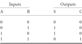
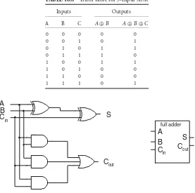
One of the basic units central to a calculator or microprocessor is a binary adder. We will consider how an adder is implemented from logic gates. A straightforward way to specify a Boolean logic function is by using a truth table. This table enumerates the output for every possible combinations of inputs. Truth tables were used inTable 16.1to specify different Boolean functions of two variables.Table 16.3shows the truth table for a Boolean operation that adds two one bit numbersAandB and produces two outputs: the sum bitSand the carry-outC. Because binary numbers can only have the values 1 or 0, adding two binary numbers each of value 1 will result in there being a carry-out. This operation is called ahalf adder. To implement the half adder with logic gates, we need to write Boolean logic equations that are equivalent to the truth table. A separate Boolean logic equation is required for each output. The most straightforward way to write an equation from the truth table is to use Sum of Products (SOP) form to specify the outputs as a function of the inputs. An SOP expression is a set of “products” (ANDs) that are “summed” (ORed) together. Note that any Boolean formula can be expressed in SOP or POS (Product of Sums) form.
Let’s consider outputS. Every line in the truth table that has a 1 value for an output corresponds to a term that is ORed with other terms in SOP form. This term is formed by ANDing together all of the input variables. If the input variable is a 1 to make the output 1, the variable appears as is in the AND term. If the input is a zero to make the output 1, the variable appears negated in the AND term. Let’s apply these rules to the half adder. TheSoutput has two combinations of inputs that result in its output being 1; therefore, its SOP form has two terms ORed together. TheCoutput only has one AND or product term, because only one combination of inputs results in a 1 output. The entire truth table can be summarized as:
S=A·B+A·B C=A·B
Note that we are implicitly using the fact that A and B are Boolean inputs. The equation for C can be read “Cis 1 whenAandBare both 1.” We are assuming thatCis zero in all other cases. From the Boolean
TABLE 16.3 Truth Table for a Half Adder
Inputs Outputs
A B S C
0 0 0 0
0 1 1 0
1 0 1 0
A
B S
C
FIGURE 16.7 The gate level implementation of a half adder.
TABLE 16.4 Binary Representation of Decimal Numbers
Decimal Binary
0 000
1 001
2 010
3 011
4 100
5 101
6 110
7 111
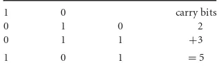
TABLE 16.5 Adding 3-Bit Binary Numbers
1 0 carry bits
0 1 0 2
0 1 1 +3
1 0 1 =5
logic equations, it is straightforward to implementSandCwith logic gates, as shown as in Figure 16.7. The logical function forSis that of an XOR gate, so we showSas an XOR gate in the figure.
The half adder is a building block in an n-bit binary adder. An n-bit binary adder adds n-bit numbers represented in base 2. Table 16.4 shows the representation of 3-bit, unsigned binary numbers. The leftmost bit is the most significant bit. It is in the 4’s place. The middle bit represents the 2’s place and the rightmost bit represents the 1’s place. The largest representable number, 1112represents 4+2+1 or 7 in decimal.
Let’s examine adding two binary numbers. Table 16.5 shows the operation 2+3=5 in binary. The top row is the carry-out from the addition in the previous bit location. Notice that there is a carry-out bit with value 1 from the second position to the third (leftmost) bit position.
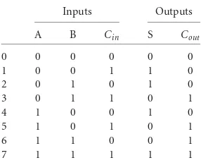
The half adder described above has two inputs:AandB. This can be used for the rightmost bit where there is no carry-in bit. For other bit positions we use afull adderwith inputsA,B, andCinand outputs
S andCout. The truth table for the full adder is given inTable 16.6.Note that a full adder adds one bit
position; it isnotan n-bit adder.
To realize the full adder as a circuit we need to design it using logic gates. We do this in the same manner as with the half adder, by writing a logic equation for each of the outputs separately. For each 1 in the truth table on the output of the function, there is an AND term in the Sum of Products representation. Thus, there are four AND terms for the S equation and four AND terms for theCoutequation. These equations
are given below:
S=A·B·Cin+A·B·Cin+A·B·Cin+ABCin Cout=A·BCin+A·B·Cin+AB·Cin+ABCin
These equations forSandCoutare logically correct, but we would also like to use the minimum number
TABLE 16.6 Truth Table for a Full Adder
Inputs Outputs
A B Cin S Cout
0 0 0 0 0 0
1 0 0 1 1 0
2 0 1 0 1 0
3 0 1 1 0 1
4 1 0 0 1 0
5 1 0 1 0 1
6 1 1 0 0 1
7 1 1 1 1 1
hence the smaller amount of power that is dissipated. Next, we will look at applying the rules of Boolean logic to minimize our logic equations.
16.4.2 Axioms and Theorems of Boolean Logic
Our goal is to use the minimum number of logic gates to implement a design. We use logic rules or axioms. These were first described by George Boole, hence the term Boolean algebra. Many of the axioms and theorems of Boolean algebra will seem familiar because they are similar to the rules you learned in algebra in high school. Let us be formal here and state the axioms:
1. Variables are binary. This means that every variable in the algebra can take on one of two values and these two values are not the same. Usually, we will choose to call the two values 1 and 0, but other binary pairs, such as TRUE and FALSE, and HIGH and LOW, are widely used and often more descriptive. Two binary operators, AND (·) and OR (+), and one unary operator, NOT, can transform variables into other variables. These operators were defined inTable 16.2.
2. Closure: The AND or OR of any two variables is also a binary variable. 3. Commutativity:A·B=B·AandA+B =B+A.
4. Associativity: (A·B)·C = A·(B·C) and (A+B)+C =A+(B+C). 5. Identity elements:A·1=1·A= AandA+0=0+A=A.
6. Distributivity:A·(B+C)= A·B+A·C andA+(B·C)=(A+B)·(A+C). (The usual rules of algebraic hierarchy are used here where·is done before+.)
7. Complementary pairs:A·A=0 andA+A=1.
These are the axioms of this algebra. They are used to prove further theorems. Each algebraic relationship in Boolean algebra has adual. To get the dual of an axiom or a theorem, one simply interchanges AND and OR as well as 0 and 1. Because of this principle ofduality, Boolean algebra axioms and theorems come in pairs. The principle of duality tells us that if a theorem is true, then its dual is also true.
In general, one can prove a Boolean theorem by exhaustion — that is, by listing all of the possible cases — although more abstract algebraic reasoning may be more efficient. Here is an example of a pair of theorems based on the axioms given above:
Theorem 16.1 (Idempotency). A·A=A and A+A= A.
Proof 16.1 The definition of AND inTable 16.1can be used with exhaustion to complete the proof for the first form.
Cout
Cout
A B Cin
A
B
C
FIGURE 16.8 The direct and reduced circuits for computing the carry-out from the three inputs to the full adder.
Now let us consider reducing the expression from the previous section:
Cout=A·BCin+A·B·Cin+AB·Cin+ABCin
First we apply idempotency twice to triplicate the last term on the right and put the extra terms after the first and second terms by repeated application of axiom 3:
Cout= A·BCin+ABCin+A·B·Cin+ABCin+AB·Cin+ABCin
Now we apply axioms 4, 3, and 6 to obtain:
Cout=(A+A)BCin+A(B+B)Cin+AB(C+C)
And finally, we apply axioms 7 and 5 to obtain:
Cout=AB+ACin+BCin
The reduced equation certainly looks simpler; let’s consider the gate representation of the two equations. This is shown inFigure 16.8.From four 3-input ANDs to three 2-input ANDs and from a 4-input OR to a 3-input OR is a major saving in a basically simple circuit.
The reduction is clear. The savings in a chip containing more than a million gates should build some enthusiasm for gate simplification. What is probably not so clear is how you could know that the key to all of this saving was knowing to make two extra copies of the fourth term in the direct expression. It turns out that there is a fairly direct way to see what you have to do, one that takes advantage of the eye’s remarkable ability to see a pattern. This tool, theKarnaugh map, is the topic of the next section. ✷
16.4.3 Design, Gate-Count Reduction, and SOP/POS Conversions
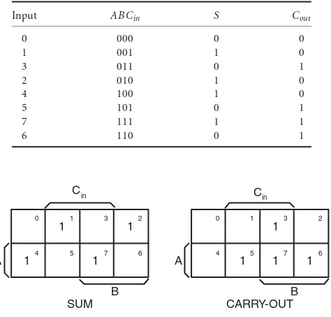
Thetruth tablefor the full adder was given isTable 16.6.All possible combinations of the three input bits appear in the second through fourth columns. Note that the first column is thenumerical valueif I interpret those three bits as an unsigned binary number. So, 000 is the value 0, 101 is the value 5, etc.
Let’s rearrange the rows of the truth table so that rather than being in increasing numerical order, the truth table values are listed in a way that each row differs from its neighbors by only one bit value. (Note that the fourth and fifth rows (entries for 2 and 4) differ by more than one bit value.) It should become apparent soon why you would want to do this. The result will beTable 16.7.
Consider the last two lines in Table 16.7, corresponding to 6 and 7. Both haveCout=1. On the input
TABLE 16.7 Truth Table for Full Adder with Rows Rearranged
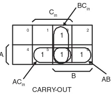
FIGURE 16.9 Karnaugh maps for SUM and CARRY-OUT. The numbers in the cell corners give the bit patterns of ABCin. The cells whose outputs are 1 are marked; those whose outputs are 0 are left blank.
The algebraic reduction operation shows up as adjacency in the table. In the same way, the 5,7 pair can be reduced. The two are adjacent and bothCoutoutputs are 1. It is less obvious in the truth table,
but notice that 3,7 also forms just such a pair. In other words, all of the steps proposed in algebra are “visible” in this truth table. To make adjacency even clearer, we arrange the groups of four, one above the other, in a table called a Karnaugh map after its inventor, M. Karnaugh [1953]. In this map, each possible combination of inputs is represented by a box. The contents of the box are the output for that combination of inputs. Adjacent boxes all have numerical values exactly one bit different from their neighbors on any side. It is customary to mark the asserted outputs (the 1’s) but to leave the unasserted cells blank (for improved readability). The tables forSandCoutare shown in Figure 16.9. The two rows are just the first
and second group of four from the truth table with the output values of the appropriate column. First convince yourself that each and every cell differs from any of its neighbors (no diagonals) by precisely one bit. The neighbors of an outside cell include the opposite outside cell. That is, they wrap around. Thus, 2 and 0 or 4 and 6 are neighbors. The Karnaugh map (or K-map) simply shows the relationships of the outputs of conjugate pairs, which are sets of inputs that differ in exactly one bit location. The item that most people find difficult about K-maps is the meaning and arrangement of the input variables around the map. If you think of these input variables as the bits in a binary number, the arrangement is more logical. The difference between the first four rows of the truth table and the second four is thatAhas the value 0 in the first four and the value 1 in the second four. In the map, this is shown by havingAindicated as asserted in the second row. In other words, where the input parameter is placed, it is asserted. Where it is not placed, it is unasserted. Accordingly, the middle two columns are those cells that haveCinasserted.
The right two columns haveBasserted. Column 3 has bothBandCinasserted.
Let us look at how the carry-out map implies gate reduction while sum’s K-map shows that no reduction is possible. Because we are looking for conjugate pairs of asserted cells, we simply look for adjacent pairs of 1’s. The carry-out map has three such pairs; sum has none. We take pairs, pairs of pairs, or pairs of pairs of pairs — any rectangular grouping of 2n cells with all 1’s. With carry-out, this gives us the groupings
A
B Cin
0 1 3 2
4 5 7 6
1
1 1
1
CARRY-OUT BCin
ACin AB
FIGURE 16.10 The groupings of conjugate pairs in CARRY-OUT.
The three groupings do the three things that we must always achieve:
1. The groups must cover all of the 1’s (and none of the 0’s).
2. Each group must include at least one cell not included in any other group. 3. Each group must be as large a rectangular box of 2ncells as can be drawn.
The last rule says that in Figure 16.10 none of these groups can cover only one cell. Once we fulfill these three rules, we are assured of a minimal set, which is our goal. Although there is no ambiguity in the application of these rules in this example, there are other examples where more than one set of groups results in a correct, minimal set. K-maps can be used for functions of up to six input variables, and are useful aids for humans to minimize logic functions. Computer-aided design programs use different techniques to accomplish the same goal.
Writing down the solution once you have done the groupings is done by reading the specification of the groups. The vertical pair in Figure 16.10 isBCin. In other words, that pair of cells is uniquely defined as
havingBandCinboth 1. The other two groups are indicated in the figure. The sum of those three (where
“+” is OR) is the very function we derived algebraically in the last section. Notice how you could know to twice replicate cell 7. It occurs in three different groups. It is important to keep in mind that the Karnaugh map simply represents the algebraic steps in a highly visual way. It is not magical or intrinsically different from the algebra.
We have used the word “cell” to refer to a single box in the K-map. The formal name for a cell whose value is 1 is themintermof the function. Its counterpart, themaxterm, comprises all the cells that represent an output value of 0. Note that all cells are both possible minterms and possible maxterms.
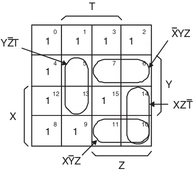
Two more examples will complete our coverage of K-maps. One way to specify a function is to list the minterms in the form of a summation. For example,Cout = (2, 5, 6, 7). Consider the arbitrary
four-input functionF(X,Y,Z,T) =
(0, 1, 2, 3, 4, 8, 9, 12, 15). With four input variables, there are 16 possible input states, and every minterm must contact four neighbors. That can be accomplished in a 4×4 array of cells as shown inFigure 16.11.Convince yourself that each cell is properly adjacent to its neighbors. For example, 1110(1011) is adjacent to 15 (1111), 9 (1001), 1010(1010), and 3 (0011) with each neighbor differing by one bit. Now consider the groupings. Minterm 15 has no neighbors whose value is 1. Hence, it forms a group on its own, represented by the AND of all four inputs. The top row and first columns can each be grouped as a pair of pairs. It takes only two variables to specify such a group. For example, the top row includes all terms of the form 00x x, and the first column includes all the terms of the formx x00. This leaves us but one uncovered cell, 9. You might be tempted to group it with its neighbor, 8, but rule 3 demands that we make as large a covering as possible. We can make a group of four by including the neighbors 0 and 1 on top. Had we not done that, the bottom pair would beX·Y·Z; but by increasing the coverage, we get that down toY·Z, a 2-input AND vs. a 3-input AND. The final expression is
0 1 3 2
FIGURE 16.12 The K-map for the complement ofFfrom Figure 16.11.
The above function is in Sum of Products (SOP) form because it is a set of products that are summed together. It is just as easy to generate the function with a Product of Sums (POS) where several OR gates are joined by a single AND. To get to that expression, we findF, the complement ofF, and then convert toF using De Morgan’s theorem.F is obtained by grouping the cells whereF is not asserted — the zero cells. This is shown in Figure 16.12, where we get the expressionF =XY Z+X Z T+XY Z+Y ZT.
Let us convert fromF toF using De Morgan’s theorem to get the POS form:
F =(XY Z+X Z T+XY Z+Y ZT)
=(X+Y+Z)(X+Z+T)(X+Y+Z)(Y+Z+T)
FIGURE 16.13 Segmente of the seven-segment display whose decoder we are going to minimize.
FIGURE 16.14 Minimization of Se without and with deliberate assignment of thedon’t cares.
16.4.4 Minimizing with Don’t Cares
Sometimes, we can guarantee that some combination of inputs will never occur. I don’t care what the output value is for that particular combination of inputs because I know that the output can never occur. This is known as an “output” don’t care. I can set these outputs to any value I want. The best way to do this is to set these outputs to values that will minimize the gate count of the entire circuit.
An example is the classic seven-segment numerical display that is common in watches, calculators, and other digital displays. The input to a seven-segment display is a number coded in binary-coded-decimal (BCD), a 4-bit representation with 16 possible input combinations, but only the 10 numbers 0,. . ., 9 ever occur. The states 10,. . ., 15 are calleddon’t cares. One can assign them to achieve minimum gate count. Consider the entire number set that one can display using seven line segments. We will consider the one line segment indicated by the arrows in Figure 16.13. It is generally referred to as “segmente,” and it is asserted only for the numbers 0, 2, 6, and 8.
Now we will minimize Se(A,B,C,D) with and without the use of thedon’t cares. We put an “X” wherever thedon’t caresmay lie in the K-map and then treat each one as either 0 or 1 in such a way as to minimize the gate count. This is shown in Figure 16.14.
We are not doing something intrinsically different on the right and left. On the left, all of thedon’t cares are assigned to 0. In other words, if someone enters a 14 into this 0 : 9 decoder, it will not light up segment e. But because this is adon’t careevent, we examine the map to see if letting it light up on 14 will help. The grouping with the choice ofdon’t carevalues is decidedly better. We choose to asserteonly fordon’t cares10 and 14, but those assignments reduce the gates required from two 3-input ANDs to two 2-input ANDs. For this little circuit, that is a substantial reduction.
16.4.5 Adder/Subtractor
Let’s return to the design of the full adder. A full (one-bit) adder can be implemented out of logic gates by implementing the equations forCandS. As we have seen, the simplified version forCis:
TABLE 16.8 Truth Table for 3-Input XOR
FIGURE 16.15 Implementation of full adder from logic gates on the left. Symbol of full adder on the right.
A B
FIGURE 16.16 Implementation of ann-bit adder from full adders.
Scannot be simplified using K-maps. Instead, we will simplifySby inspection of the truth table for the full-adder given inTable 16.6.Note thatSis high when exactly one of the three inputs is high, or when all the inputs are high. This is the same functionality as a 3-input XOR gate, as shown inTable 16.8.Thus we can implementSwith the equation:
S=A⊕B⊕ Cin
TABLE 16.9 Binary Representation of Negative Numbers
Decimal Sign-Magnitude 1’s Complement 2’s Complement
7 0111 0111 0111
6 0110 0110 0110
5 0101 0101 0101
4 0100 0100 0100
3 0011 0011 0011
2 0010 0010 0010
1 0001 0001 0001
0 0000 0000 0000
−0 1000 1111
−1 1001 1110 1111
−2 1010 1101 1110
−3 1011 1100 1101
−4 1100 1011 1100
−5 1101 1010 1011
−6 1110 1001 1010
−7 1111 1000 1001
−8 1000
16.4.6 Representing Negative Binary Numbers
We would like to add negative numbers as well as positive numbers, and we would like to subtract numbers as well as add them. To do this we need a way of representing negative numbers in base 2. Two common methods are used:sign-magnitudeand2’s complement. A third method,1’s complementwill also be described to aid in the explanation of 2’s complement.
In Table 16.9, four bits are used to represent the values 7 to 0. The three different methods, for repre-senting negative numbers are shown. Note that forallthree methods, the positive numbers have the same representation. Also, the leftmost bit is always the sign bit. It is 0 for a positive number and 1 for a negative number. It is important to note that all these representations are different ways that ahumaninterprets the bit patterns. The bit patterns are not what is changing; the interpretations are. Given a bit pattern, you cannot tell which system is being used unless someone tells you. This discussion can be extended to numbers represented with any number of bits.
The sign-magnitude method is the closest to the method we use for representing positive and negative numbers in decimal. The sign bit indicates whether it is positive or negative, and the remaining bits represent the magnitude or value of the number. So, for example, to get the binary value of negative 3, you take the positive value 0011 and flip the sign bit to get 1011. While this is the most intuitive for humans to understand, it is not the easiest representation for computers to manipulate. This is true for several reasons. One is that there are two representations for 0:+0 and−0. A very common operation to perform is to compare a number to 0. With two representations of zero, this operation becomes more complex.
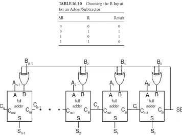
TABLE 16.10 Choosing the B Input
FIGURE 16.17 Connection of n full adders to form anN-bit ripple-carry adder/subtractor. At the rightmost adder, the subtract line (SB) is connected to Cin0.
with 4 bits, this leaves me with a non-symmetric range. In other words, I can represent one more negative number 1000 than positive number. This number is−8. Its positive value cannot be represented in 4 bits. What happens if I take the 2’s complement of−8 ? The 1’s complement is 0111. When I add 1 to form the 2’s complement, I get 1000. What is really happening is that the true value,+8, cannot be represented in the number of bits I have available. It overflows the range for the representation I am using.
Representing numbers in 2’s complement makes it easy to do subtraction. To subtract two n-bit numbers A−B, you simply invert the bits ofBand add 1 when you are summingA+B.
We are now ready to expand our n-bit ripple carry adder to an n-bit adder/subtractor. Just as we do addition one digit at a time, the adder circuit handles two input bits,AiandBi, plus a carry-inCini. We can arrange as many of these circuits in parallel as we have bits. Theith circuit gets theith bits of two operands plus the carry-out of the previous stage. It is straightforward to modify the full-adder to be a one-bit adder/subtractor. A one-bit adder/subtractor performs the following tasks:
1. ChooseBior the complement ofBias theBinput.
2. Form the sum of the three input bits,Si =Ai+Bi+Cini. 3. Form the carry-out of the three bits,Couti = f(Ai,Bi,Ci ni).
On a bit-by-bit basis, the complement of Bi is justBi. For an n-bit number, the 2’s complement is
formed by taking the bit-by-bit complement and adding 1. I can add 1 to an n-bit subtraction by setting the carry-in bitCi n0to 1. In other words, I wantCi n0 =1 when subtract is true, andCi n0=0 when subtract
is false. This is accomplished by connecting the control signal for subtracting (SB) toCi n0. Similarly when
SB = 0, I want to use Bi as the input to my full adder. When SB = 1, I want to useBi as input. This is
summarized inTable 16.10.By inspection, the desired B input bit to theith full adder is the XOR ofS B andBi. If I put all the components together —nfull adders, the carry-in of the LSB set toS B, and the XOR
TABLE 16.11 Truth Table for a 4-to-2 Encoder
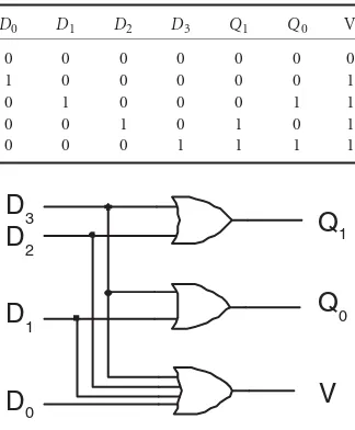
D0 D1 D2 D3 Q1 Q0 V
0 0 0 0 0 0 0
1 0 0 0 0 0 1
0 1 0 0 0 1 1
0 0 1 0 1 0 1
0 0 0 1 1 1 1
V
Q
1Q
0D
3D
2D
1D
0FIGURE 16.18 A 4-to-2 encoder with outputsQ0andQ1and valid signal.
16.5 Frequently Used Digital Components
Many components such as full adders, half adders, 4-bit adders, 8-bit adders, etc., are used over and over again in digital logic design. These are usually stored in a design library to be used by designers. In some libraries these components are parameterized. For example, a generator for creating ann-bit adder may be stored. When the designer wants a 6-bit adder, he or she must instantiate the specific bit width for the component.
Many other, more complex components are stored in these libraries as well. This allows components to be designed efficiently once and reused many times. These include encoders, multiplexers, demultiplexers, and decoders. Such designs are described in more detail below. Later, we will use them in the design of a calculator datapath.
16.5.1 Elementary Digital Devices: ENC, DEC, MUX, DEMUX
16.5.1.1 ENC
An ENCODER circuit has 2ninput lines and
noutput lines. The output is the number of the input line that is asserted. Such a circuitencodesthe asserted line. The truth table of a 4-to-2 encoder is shown in
Table 16.11.The inputs areD0,D1,D2, andD3, and the outputs areQ0andQ1. Note that we assume at most one input can be high at any given time. More complicated encoders, such as priority encoders, that allow more than one input to be high at a time, are described below.
An encoder, like all other components, is built out of basic logic gates. The equations for theQoutputs can be determined by inspection.Q0is 1 ifD1is 1 orD3is 1.Q1is 1 ifD2is 1 orD3is 1.
Note that there is no difference in the outputs of this circuit ifnoinput is asserted, or if inputD0is asserted. To distinguish between these two cases, an output that indicates theQ outputs are valid,V is added.Vis 1 if any of the inputs are 1, and 0 otherwise.V is considered a control output rather than a data output. A logic diagram of an encoder is shown in Figure 16.18.
16.5.1.2 DEC
TABLE 16.12 Truth Table for a 2-to-4 Decoder with Enable
EN A B Q0 Q1 Q2 Q3
0 X X 0 0 0 0
1 0 0 1 0 0 0
1 1 0 0 1 0 0
1 0 1 0 0 1 0
1 1 1 0 0 0 1
the enable input (EN) is 0, the circuit is disabled, and all outputs are 0. The truth table of a 2-to-4 decoder is given in Table 16.12.
Note the use of X values for inputs in the first line of the truth table. Here, X stands for “don’t care.” In other words, I don’t care what the value of the inputs A and B are. IfEN=0, the outputs will always have the value 0. I am using thedon’t caresymbol, X, as a shorthand for the four combinations of input values for A and B. We have already useddon’t caresfor minimizing circuits with K-maps above. In that case, the don’t careswere “output”don’t cares. Thedon’t caresin the truth table for the encoder are “input”don’t cares. They are shorthand for several combinations of inputs.
16.5.1.3 MUX
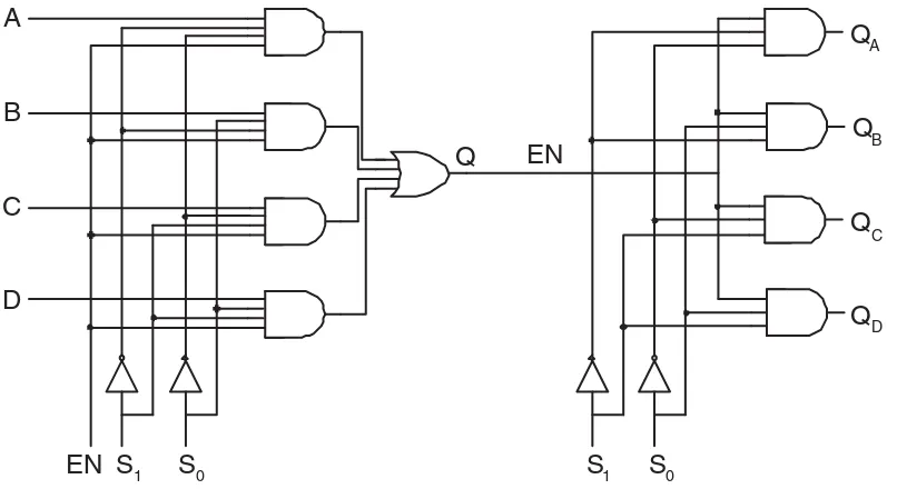
Many systems have multiple inputs which are handled one at a time.Call waitingis an example. You are talking on one connection when a clicking noise signals that someone else is calling. You switch to the other, talk briefly, and then switch back. You can toggle between calls as often as you like. Because you are using one phone to talk on two different circuits, you need amultiplexeror MUX to choose between the two. There is also an inverse MUX gate called either a DEMUX or a DECODER. Again, a telephone example is the selection of an available line among, say, eight lines between two exchanges. That is, you have one line in and eight possible out, but only one output line is connected at any time. An algorithm based on which lines are currently free determines the choice. Let us design these two devices, beginning with a 2-to-1 MUX.
What we want in a two-input MUX is a circuit with one output. The value of that output should be the same as the input that we select. We will call the two inputsAandBand the outputQ. The select input Schooses which input to steer to the output.
Logically I can think ofQbeing equal toAwhenS =0, andQbeing equal toBwhenS =1. I can write this as the Boolean equation:Q=(A·S)+(B·S). You can use a truth table to convince yourself that this equation captures the behavior of a two-input MUX. Note that we now have a new dichotomy of inputs. We call some of them inputsand the otherscontrols. They are not inherently different, but from the human perspective, we would like to separate them. In logic circuit drawings,inputscome in from the left and outputs go out to the right.Controlsare brought in from top or bottom. The select input for our multiplexer is a control input. Note that, although I talk about S being a control, in the logic equation it is treated the same as an input. An enable is another kind of control input. A valid signal can be viewed as a control output. A realization of a 2-to-1 multiplexer with enable is shown in Figure 16.19.
The 2-to-1 MUX circuit is quite useful and is found in many design libraries. Other similar circuits are the 4-to-1 MUX and the 8-to-1 MUX. In general, you can design n-to-1 MUX circuits, where n is a power of 2. The number of select bits needed for an n-to-1 MUX isl og2(n).
A
B
S
Q
EN
FIGURE 16.19 A 2-to-1 MUX with enable. If the enable is asserted, this circuit delivers at its output,Q, the value of Aor the value ofB, depending on the value ofS. In this sense, the output is “connected” to one of the input lines. If the enable is not asserted, the outputQis low.
A
B
S
1Q
EN
C
D
S
0EN
S
1S
0Q
AQ
BQ
CQ
DFIGURE 16.20 A 4-to-1 MUX feeding a 1-to-4 DEMUX. The value on MUX select lines S1:S0 determines the input connected toQ.EN, in turn, is connected to the output of choice by S1:S0 on the DEMUX.
16.5.1.4 DEMUX/DECODER
The inverse circuit to a multiplexer is a demultiplexer, or DEMUX. A DEMUX has one line in, which it switches to one of n possible output lines. A 1-to-4 DEMUX, used in conjunction with the 4-to-1 MUX, is shown on the right in Figure 16.20.
Note that theQoutput line on the multiplexer is labeled as theENinput line on the DEMUX. If I treat this line as anenable, the DEMUX becomes a DECODER, in the sense that, whenENis asserted, one and only one of the four outputs is asserted, that being the output selected by the number on S1:S0. So a decoder and a demux are the same circuit. You usually do not find a demux in a design library. Rather, what you find is called a decoder, or sometimes a demux/decoder.
TABLE 16.13 Truth Table for a 4-to-2 Priority Encoder
D0 D1 D2 D3 Q0 Q1 V
0 0 0 0 0 0 0
1 0 0 0 0 0 1
X 1 0 0 1 0 1
X X 1 0 0 1 1
X X X 1 1 1 1
TABLE 16.14 ALU Instructions for Calculator
I1 I0 Result
0 0 AANDB
0 1 AORB
1 0 A+B
1 1 A−B
instructions are numbers that must be decoded to assert the lines which enable the specific hardware that each instruction requires.
16.5.1.5 Priority Encoder
The encoder we started this section with assumed that exactly one input was asserted at any given time. An encoder that could deal with more than one asserted input would be even more useful, but how would we define the output if more than one line were asserted? One simple choice is to have the encoder deliver the value of the highest-ranking line that is asserted. Thus, it is apriority encoder.
The truth table for the priority encoder is given in Table 16.13. This truth table has a lot of similarities to the simple encoder we started this section with. The valid outputVtells us if any input is asserted. The outputQ0is true if the only input asserted isD1. The circuit differs in that more than one input may be asserted. In this case, the output encodes the value of the highest input that is asserted. So, for example, ifD0andD1are both asserted, the outputQ0is asserted. I don’t care if the D0input is asserted or not, because theD1input has higher priority. Here, once again, thedon’t caresare used as shorthand to cover several different inputs. If I listed all possible combinations of inputs in the truth table, my truth table would have 24=16 lines. Usingdon’t caresmakes the truth table more compact and readable.
16.5.2 The Calculator Arithmetic and Logical Unit
Let’s look at putting some of these components together to do useful work. The core of a calculator or microprocessor is its Arithmetic and Logic Unit (ALU). This is the part of the calculator that implements the arithmetic functions, such as addition, subtraction, and multiplication. In addition, logic functions are also implemented such as ANDing inputs and ORing inputs. A microprocessor may have several, sophisticated ALUs. We will examine the design of a very simple ALU for a 4-bit calculator. Our ALU will perform four different operations: AND, OR, addition, and subtraction on two 4-bit inputs,AandB. Two input control signals,I1andI0, will be used to choose between the operations, as shown inTable 16.14.
We will call the 4-bit resultR.
ADD/SUB
A3A2A1A0 B3B2B1B0
S3 S2 S1 S0
ANDs
A3A2A1A0 B3B2B1B0
T3 T2 T1 T0 A3 -0
B3-0
MUX
R3
MUX
R2
MUX
R0
MUX
R1 I1
I0
ORs
A3A2A1A0 B3B2B1B0
U3 U2 U1 U0
SB
A3 A2 A1 A0
FIGURE 16.21 Implementation of an ALU from other components.
ALU
B3B2B1I0
A3A2A1A0
R3 R2 R1 R0
I1 B0
FIGURE 16.22 Symbol of an ALU component.
there are no 3-to-1 muxes. We will use the fourth input to pass theAinput to the outputR. The reason for doing this will become apparent when we use the ALU in a calculator datapath. To keep the diagram readable, we use the convention that signals with the same name are wired together. The resulting ALU implementation is shown in Figure 16.21. The symbol for this ALU is shown in Figure 16.22. We will use this symbol when we incorporate the ALU into a calculator datapath.
16.6 Sequential Circuits
16.6.1 Concept of a Sequential Device
One of the oldest and most familiar sequential devices is a clock. In its mechanical implementation, ticks from a mechanical oscillator — pendulum or spring and balance wheel — are tallied in a complex, base-12 counter. Typically, the counter recycles every 12 hours. All the states are specifiable, and they form an orderly sequence. Except during transitions from one state to its successor, the clock is always in a discrete state. To be in a discrete state requires some form of memory. I can only know the current output of my clock if I know what its previous output was.
One of the most ubiquitous and essential memory elements in the digital world is the latch, or flip-flop. It snaps from one position to the other (storing a 1 or storing a 0) and retains memory of its current position. We shall see how to build such a latch out of logic gates.
Like clocks, computers and calculators arefinite-state machines. All of the states of a computer can be enumerated. Saying this does not in any way restrict what you can compute anymore than saying you can completely describe the states of a clock limits the life of the universe. The states of a finite-state machine capture the history of the behavior of the circuit up to the current state.
By linking memory elements together, we can build predictable sequential machines that do important and interesting tasks. Only the electronic “latch” and the datapath of our simple calculator are included in this short chapter; but from the sequential elements presented here, complex machines can be built. There are two kinds of sequential circuits, calledclockedor synchronous circuits andasynchronouscircuits. The clocked circuits are built from components such as the flip-flop, which are synchronized to a common clock signal. In asynchronous circuits, the “memory” is the intrinsic delay between input and output. To maintain an orderly sequence of events, they depend on knowing precisely how long it takes for a signal to get from input to output. Although that sounds difficult to manage in a very complex device, it turns out that keeping a common clock synchronized over a large and complex circuit is nontrivial as well. We will limit our discussion to clocked sequential circuits. They are more common, but as computer speeds become faster, the asynchronous approach is receiving greater attention.
16.6.2 The Data Flip-Flop and the Register
16.6.2.1 TheSRLatch: Set, Reset, Hold, and Muddle
In all the circuits we have looked at so far, there was a clear distinction between inputs and outputs. Now we will erase this distinction by introducing positive feedback; we willfeed backthe outputs of a circuit to the inputs of the same circuit. In an electronic circuit, positive feedback can be used to force the circuit into a “stable state.” Because saturated logic goes into such states quite normally, it is a very small step to generate an electronic latching circuit from a pair of NAND or NOR gates. The simplest such circuit is shown in Figure 16.23.
Analyzing Figure 16.23 requires walking through the behavior of the circuit. Let’s assume thatQhas the value 1 andQhas the value 0. Start with bothSand Rdeasserted. In other words, both have value 1 because they are active low signals. The inputs toBwill be high, soQwill be low. This is a “steady state”
S
R
Q
Q
A
B
A
B
NAND
0
0
1
0
1
1
1
0
1
1
1
0
of this circuit; the circuit will stay in this state for some time. This state is called “storing 1,” or sometimes just “1” becauseQhas the value 1. You could toggleS(i.e., change its value to 0 and then back to 1) and no other change would take place in the circuit.
Now, withShigh, let’s assertRby setting it to 0. First,Qwill go high becauseRis one of the inputs to B, and the NAND of 0 with anything is 1. This makes both of the inputs toAhigh, soQgoes low. Now the upper input toBis low, so deassertingR(setting it to 1) will have no effect. Thus, assertingRhas reset the latch. The latch is in the other steady state, “storing 0” or “0.”
At this point, assertingSwill set the latch, or put it back into the state “1.” For this reason, theSinput is the “set” input to the latch, and theRinput is the “reset” input.
What happens if bothSandRare asserted at the same time? The initial result is to have bothQandQ go high simultaneously. Now, deassert both inputs simultaneously. What happens? You cannot tell. It may go into either the set or the reset state. Occasionally, the circuit may even oscillate, although this behavior is rare. For this reason, it is usually understood that the designer isnot allowedto assert bothSand Rat the same time. This means that, if the designer asserts bothSandRat the same time, the future behavior of the circuit cannot be guaranteed, until it is set or reset again into a known state.
There is another problem with this circuit. To hold its value, both S and R must be continuously deasserted. Glitches and other noise in a circuit might cause the state to flip when it should not.
With a little extra logic, we can improve upon this basic latch to build circuits less likely to go into an unknown state, oscillate, or switch inadvertently. These better designs eliminate the muddle state.
16.6.2.2 The TransparentD-Latch
A simple way to avoid having someone press two buttons at once is to provide them with a toggle switch. You can push it only one way at one time. We can also provide a single line to enable the latch. This enable control signal is usually called theclock. We will modify the SR latch above. First we will combine the S and R inputs into one input called the data, orDinput. When theDline is a 1, we will set the latch. When theDline is a 0, we will reset the latch. Second, we will add a clock signal (CLK) to control when the latch updates. With the addition of two NANDs and an inverter, we can accomplish both purposes, as shown inFigure 16.24.
Note that we tie the data line,D, to the top NAND gate, and the inverse orDto the bottom NAND gate. This assures that only one of the two NAND outputs can be low at one time. The CLK signal allows us to open the latch (let data through) or latch the data at will. This device is called a transparent D-latch, and is found in many digital design libraries. This latch is calledtransparentbecause the current value of D appears at Q if the CLK signal is high. If CLK is low, then the latch retains the last valueDhad when CLK was high.
Has this device solved all the problems we described for theSRlatch? No. Consider what might happen ifDchanges from low to high just as the clock changes from high to low. For the brief period before the change has propagated through theD-inverter, both NANDs see both inputs high. Thus, at least briefly,
S
R
Q
Q
D
CLK
Q D
CLK
Q Q D
S1 S2
R2 R1
FIGURE 16.25 The master–slave data flip-flop constructed of two D-latches in series.
bothRandSare asserted. This is the very situation we wanted to avoid. This muddle situation would last only for the propagation time of the inverter, but then the CLK signal arrives and drives bothSand R high. The latch might oscillate or flip either way. In any case, it will be unpredictable.
There is another problem with this circuit. It is indeed transparent during the high clock signal. This means thatQwill mirrorDwhile CLK is high. IfDchanges rapidly, so willQ. Sometimes you may want transparency. However, frequently you want to be able to guarantee when the output will change and to only allow one transition on the output per clock cycle. In that case, you do not want transparency; what you really want is a different circuit: a flip-flop (FF).
16.6.2.3 Master--Slave DFF to Eliminate Transparency
The problem with transparent gates is not a new one. A solution that first appeared in King Solomon’s time (9th century B.C.E.) will work here as well. The Solomonic gate was a series pair of two quite ordinary city gates. They were arranged so that both were never open at the same time. You entered the first and it was shut behind you. While you were stuck between the two gates, a well-armed, suspicious soldier asked your business. Only if you satisfied him was the second gate opened. The solution of putting out-of-phase transparent latches between input and output is certainly one obvious solution to generating a data flip-flop(DFF). Such an arrangement of twoD-latches is shown inFigure 16.25.
The latch on the left is called themaster; that on the right is called theslave. This master–slave (MS) DFF solves the transparency problem but does nothing to ameliorate the timing problems. While timing problems are not entirely solvable in any FF, accommodating the number of delays in this circuit tends to make the MSFF a slow device and thus a less attractive solution. Why should it be slow? The issue is that to be sure that you do not put either of these devices into a metastable or oscillatory state, you must hold Dconstant for a relatively long setup time (before the clock edge) and continue it past the clock transition for a sufficient hold time. This accommodation limits the speed with which the whole system can switch. Can we do better? Yes, not perfect, but better. The device of choice is the edge-triggered DFF. We will not go into the details of the implementation of an edge-triggered flip-flop as it is considerably more complicated than the circuits considered so far. An edge-triggered flip-flop is designed to pass the input datum to the output during a very short amount of time defined by a clock edge. Edge-triggered flip-flops can either berising edgetriggered orfalling edgetriggered. A rising edge triggered flip-flop will only change its output on the rising edge of a clock. There is still a setup time and a hold time; a small amount of time right around the clock edge during which the input datum must be stable in order to avoid the flip-flop becoming metastable. The advantage of the edge-triggered design is that there is only one brief moment when any critical changes take place. This improves synchronization and leads to faster circuits.