ECE 304 Spring ’05 Lab 1
Measuring transistor
β
DC, Early voltage V
AF, and scale current I
SObjective
When we design a circuit using bipolar transistors, we use idealized equations and an idealized
transistor. PS
PICEdescribes this ideal NPN transistor using the dot-model statement in Figure 1.
.model Qidealn NPN (Bf={B_F} Vaf={V_AF} Is={I_S})
FIGURE 1
PSPICE dot-model statement for the ideal bipolar transistor: β = Bf, Early voltage Vaf, and scale current Is; as shown by curly braces {}, these values are set using variables B_F, V_AF and I_S from a PARAMETER box
However, real circuits use real transistors. An example is the Q2N2222, approximated in PS
PICEusing the dot-model statement of Figure 2.
.model Q2N2222 NPN(Is=14.34f Xti=3 Eg=1.11 Vaf=74.03Bf=255.9 Ne=1.307 + Ise=14.34f Ikf=.2847 Xtb=1.5 Br=6.092 Nc=2 Isc=0 Ikr=0 Rc=1
+ Cjc=7.306p Mjc=.3416 Vjc=.75 Fc=.5 Cje=22.01p Mje=.377 Vje=.75 + Tr=46.91n Tf=411.1p Itf=.6 Vtf=1.7 Xtf=3 Rb=10)
FIGURE 2
Dot-model statement of the Q2N2222 found by highlighting the device, right clicking, and selecting EDIT PSPICE MODEL
If we design using the ideal transistor, and build using, for example, the Q2N2222, can we expect
the built circuit to behave anything like the designed circuit? To have hope of success, our ideal
transistor should have parameter values selected to match the Q2N2222 as closely as possible.
In this lab we will determine the values of Bf, Vaf and Is that make an ideal transistor approximate
the Q2N2222.
We compare the PS
PICEresults for a Q2N2222 with an ideal transistor using the setup of
Figure 3 below.
698.5mV 0 Qidealn Q1 44.07uA 9.956mA Q2 Q2N2222 44.47uA 9.956mA 22.73V PARAMETERS:
I_E = 10mA R_B = 500k
0
DOT-MODEL
V_AF = 74.03V B_F = 174.11 I_S = 14.34fA
0 I1 {I_E} 10.00mA I2 {I_E} 10.00mA + R2 {R_B} 22.94V
.model Qidealn NPN (Bf={B_F} Vaf={V_AF} Is={I_S})
0 699.6mV + R1 {R_B} B C
FIGURE 3
Circuits for comparison of ideal transistor with shown dot-model statement with the Q2N2222; parameters IS and VAF are taken from the Q2N2222 dot-model statement, and
βDC(VCB=0V) is taken from βDC for the Q2N2222 in the PSPICE output file for this value of IE
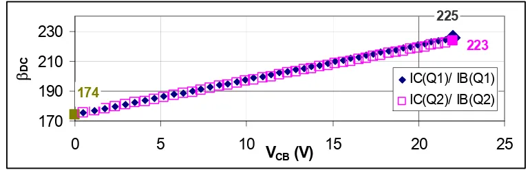
The results of the comparison are shown in Figure 4. It is clear that the two curves agree
closely as to value and slope. That is, the ideal transistor with the appropriate values of
parameters B
Fand V
AFclosely approximates the V
CBdependence of the DC
β
of the Q2N2222.
11
However, in the ideal transistor, the DC beta and AC beta values are the same, and
225
223
174
170
190
210
230
0
5
10
15
20
25
V
CB(V)
β
DC
IC(Q1)/ IB(Q1) IC(Q2)/ IB(Q2)
FIGURE 4
Comparison of βDC vs. VCB for the ideal and the Q2N2222 transistors with IE = 10 mA
Because
β
DCdepends on current in the Q2N2222 (but does not depend on current in the ideal
transistor) the value of
β
DC(V
CB= 0V) used for Bf in the ideal transistor has to be set to agree with
the PS
PICEoutput file BetaDC for the Q2N2222 at V
CB= 0V and the appropriate current. (For
example, we force fitted the point at V
CB= 0V in Figure 4). Agreement is not perfect in Figure 4
because the dot-model statement of the Q2N2222 is much more complicated than that for the
ideal transistor, as shown above in Figure 2.
To summarize, in this lab we:
1. Learn how to measure values for Bf, Vaf and Is,
2. Learn a bit about the current mirror as an approximation to an ideal current source,
3. Learn a bit about the variability of device parameters,
4. Learn that circuit design is necessarily approximate because our models aren’t perfect, and
5. Learn how to use some features of E
XCELand PS
PICEBasic idea for finding parameter values
0
0
Q2N2222
+
-{V_CB}
{I_E}
FIGURE 5
Idealized circuit for measuring DC beta and Early voltage
Figure 5 shows the basic idea behind the measurement of
β
DCand V
AF. A known emitter current
I
Eis driven into the transistor and a known collector-to-base voltage V
CBis applied. The value of
β
DCis then
EQ. 1
1 B I
E I
DC = −
β .
The value of
β
DCis plotted against V
CBand fitted to the formula of EQ. 2 below:
EQ. 2
+ = =
AF V
CB V 1 ) 0 CB V ( DC
DC β
The slope and intercept of the plot determine
β
DCat V
CB= 0V and the value of the Early voltage
V
AF.To implement EQ. 1 we need the value of the base current I
B. Therefore, we modify the
circuit as shown in Figure 6, and determine the base current from the known value of resistor R
Band the measured collector and base voltages as given in EQ. 3 below.
B C
B
0
+{R_B}
0
Q2N2222 {I_E}
FIGURE 6
Circuit of Figure 5 modified to allow measurement of base current
EQ. 3
B R
B V C V B
I = − .
Implementation of current source I
ETo apply a known current I
Eas shown in Figure 3 we build an approximate current source using
the circuit of Figure 7.
Q2 Q2N2907A
-56.96uA -12.81mA
0
+
R3
{R_R}
12.92mA +
- OUTPUT
{V_A} 12.92V
0 +
-V1
{V_CC} 25.73mA
15.00V
+
R2 {R_E}
12.86mA
13.71V
PARAMETERS:
R_E = 100
V_A = 12.92V V_CC = 15V R_R = 1k
0
12.92V
Q1 Q2N2907A
-56.96uA -12.81mA
+
R1 {R_E}
12.86mA
13.71V
FIGURE 7
Circuit for a current mirror approximating an ideal current source
The applied bias V
Ain Figure 7 has been chosen to equal the base voltage of the two transistors,
V_A
0V 5V 10V 15V
I(OUTPUT) -20mA
0A 20mA
(0.00,12.85mA) (12.92,12.81mA)
(14.37,0.00A)
FIGURE 8
I-V behavior of the current mirror of Figure 7
Examining the
I-V
behavior of Figure 7, the current is nearly constant for V
Abelow about V
B=
12.92V. As V
Agoes above this value, the current drops rapidly, because the transistor Q1
saturates, leaving the active mode. Thus, the circuit of Figure 7 is a pretty good approximation to
an ideal current source delivering 12.81mA - 12.85 mA for voltages below about V
A= V
B=
12.92V. The current level delivered by the mirror is adjusted using the resistor R
R, as is
suggested because the current in R
Ris I
R= V
B/R
Rand is nearly the same as the output current.
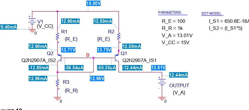
Calibration of the mirror
We cannot assume that both transistors in the mirror will be matched in the lab circuit, so we do a
calibration run to find what current we actually get for a given bias condition. For example,
suppose the two transistors have different scale currents I
Sas shown in the dot-model statements
of Figure 9 below.
.model Q2N2907A_IS1 PNP(Is={I_S1} Xti=3 Eg=1.11 Vaf=115.7 Bf=231.7 Ne=1.829 + Ise=54.81f Ikf=1.079 Xtb=1.5 Br=3.563 Nc=2 Isc=0 Ikr=0 Rc=.715
+ Cjc=14.76p Mjc=.5383 Vjc=.75 Fc=.5 Cje=19.82p Mje=.3357 Vje=.75 + Tr=111.3n Tf=603.7p Itf=.65 Vtf=5 Xtf=1.7 Rb=10)
.model Q2N2907A_IS2 PNP(Is={I_S2} Xti=3 Eg=1.11 Vaf=115.7 Bf=231.7 Ne=1.829 + Ise=54.81f Ikf=1.079 Xtb=1.5 Br=3.563 Nc=2 Isc=0 Ikr=0 Rc=.715 + Cjc=14.76p Mjc=.5383 Vjc=.75 Fc=.5 Cje=19.82p Mje=.3357 Vje=.75 + Tr=111.3n Tf=603.7p Itf=.65 Vtf=5 Xtf=1.7 Rb=10)
FIGURE 9
+ R2 {R_E} 12.50mA 13.71V DOT-MODEL
I_S1 = 650.6E-18A I_S2 = {I_S1*5}
Q2N2907A_IS2 Q2 -56.54uA -12.85mA 12.90mA 0 13.75V + R1 {R_E} 12.90mA 0 15.00V 12.96V PARAMETERS:
R_E = 100
V_A = 13.01V V_CC = 15V R_R = 1k
0 Q2N2907A_IS1 Q1 -55.35uA -12.44mA 12.50mA + -V1 {V_CC} 25.40mA + - OUTPUT {V_A} 12.44mA + R3 {R_R} 12.96mA 13.01V B
FIGURE 10
Current mirror with mismatched transistors: IS2 = 5IS1
Figure 10 shows the current mirror with mismatched transistors: the currents in the two transistors
are not the same, and the output current differs quite a bit from the current in R
R. We run an
I-V
curve like Figure 8 so we can determine exactly what current is provided to our test Q2N2222.
An example is shown in Figure 11. Using this plot we can find exactly what current is delivered if
we know the voltage V
A.
V_A
0V 5V 10V 15V
I(OUTPUT) -20mA 0A 20mA (5.000,12.46mA) (0.00,12.48mA) (13.01,12.44mA)
FIGURE 11
Calibration run for the mirror in Figure 10
Fitting procedure
We first build a mirror like Figure 10, and make an
I-V
calibration run. Then we hook up the
Q2N2222 as shown in Figure 3, using the mirror in place of the current source to provide I
E. Then
we measure V
C, V
B, R
Band determine the value of I
Efor various V
CBvalues, and put this data into
an E
XCELspreadsheet. We make a best fit to this plot using the T
RENDLINEfeature of E
XCEL, as
explained next.
DATA ENTRY
FIGURE 12
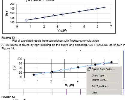
Data entered on spreadsheet and calculation made of IB, IE, VCB and βDC FITTING THE DATA
A plot is made of
β
DCvs. V
CBas shown in Figure 13.
y = 2.4023x + 180.69
180 185 190 195 200
0 1 2 3 4 5 6 7
VCB(V)
β
DC
FIGURE 13
Plot of calculated results from spreadsheet with TRENDLINE formula at top
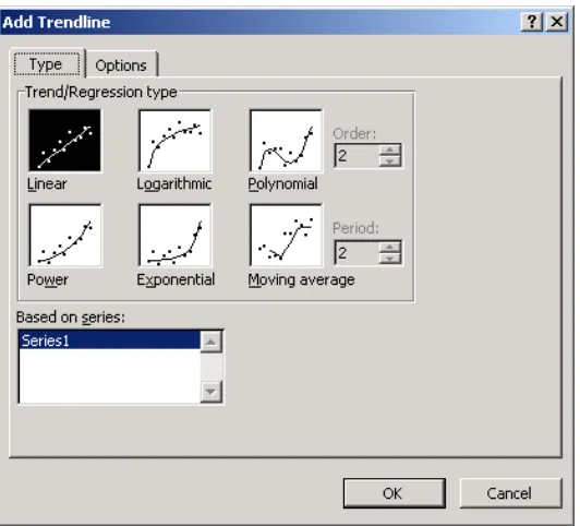
A T
RENDLINEis found by right clicking on the curve and selecting A
DDT
RENDLINE, as shown in
Figure 14.
FIGURE 14
Adding a TRENDLINE
FIGURE 15
Choosing the LINEAR trend line
FIGURE 16
Choosing to DISPLAY EQUATION on chart
With the slope and intercept from the trend line equation in the form
y = mx + b
we find the value
of
β
DC(V
CB= 0V) and V
AFusing the equations
EQ. 4
βDC(VCB = 0V) = b and VAF = b/m.
Formula Box
FIGURE 17
Calculation of βDC and VAF; the formula box shows EQ. 4
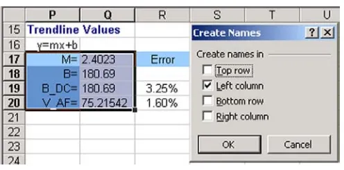
To obtain a formula in the formula box in Figure 17, we must name the variables M and B by
highlighting P17:Q20 and using the menu I
NSERT/N
AME/C
REATE. See
Figure 18
below.
FIGURE 18
Naming variables to obtain formulas in the FORMULA BOX
Another example of this procedure is shown in the
Appendix
.
The values in Figure 17 can be compared to the PS
PICEoutput file
β
DC(V
CB=0V) = 175
and V
AF= 74.03V. Accuracy is as shown in Figure 17.
This procedure should be followed for three current levels near the values 100
µ
A, 1 mA
and 10 mA, for two different Q2N2222 transistors. The results should be compared with each
other and with the manufacturer’s data sheet and the differences summarized.
Precautions
The temperature will change as the transistor heats up – allow the transistor to cool between data
points.
Finding the scale current
The base voltage of the Q2N2222 is given by
EQ. 5
= + = = = = ) E I , V 0 CB V ( 1 1 S I ) V 0 CB V ( E I n TH V S I ) V 0 CB V ( C I n TH V BE V β l l ,where V
THis the thermal voltage, 25.864mV at 27
°
C. Your transistor may be at a different
temperature: for one thing, it heats when drawing current. In EQ. 5, I
Sis the scale current. If there
is no Early effect, the current does not depend on collector-base bias V
CB, but in our ideal
transistor there is an Early effect and the current is given by EQ. 6 below. (The Q2N2222 uses a
more complex equation, approximated by EQ. 6.
2)
2
EQ. 6
+ = = AF V CB V 1 ) V 0 CB V ( C I C I .Because I
Cdepends on V
CB, using a current corresponding to V
CB> 0 in EQ. 5 will lead to an
incorrect V
BE. Also, note that in EQ. 5, the value of
β
varies with current level I
E; that is,
β
=
β
(V
CB, I
E).
According to EQ. 5, a plot of base voltage of the Q2N2222 vs.
l
n(I
E) will have a slope of
V
TH, and by doing a best fit we can find the best value of I
S. If
β
>> 1, the error in neglecting
variation of
β
with I
Ewhen plotting will not have much effect upon the value obtained for I
S. Doing
the fit with the largest and smallest
β
-value is a check on this particular error.
ENTERING THE DATA
An example worksheet for finding V
THand I
Sis shown in Figure 19 below. The measured
data is for the case V
CB= 0 V, or R
B=0
Ω
.
6 7 8 9 10 11 12 13 14 15
B C D E F G H I J K L M
Calculated Calculated Calculated Percent Percent
Fitted Values R_R I_E V_B V_TH_Q3 I_S_Q3 V_BE Error Trendline Error
V_TH 0.025868 100 0.0697 0.766 0.026100 9.7221E-15 0.7587046 0.89 0.762844 0.35 I_S 1.2678E-14 215 0.0441 0.750 0.025978 1.1193E-14 0.7468559 0.42 0.750023 0.00 B_DC 162.6 464 0.0245 0.732 0.025882 1.2458E-14 0.7316679 0.05 0.733589 0.21 B_DC(min) 148.9 1000 0.0124 0.713 0.025820 1.3320E-14 0.7140578 0.19 0.714534 0.25 B_DC(max) 176.3 2154 0.0059 0.692 0.025784 1.3806E-14 0.6947137 0.33 0.693602 0.17 4642 0.0026 0.671 0.025763 1.4061E-14 0.6738291 0.41 0.671004 0.01 10000 0.0011 0.648 0.025751 1.4186E-14 0.6508884 0.46 0.646181 0.27 Averages 0.025868 1.2678E-14 Total Error 2.74 1.26
FIGURE 19
Worksheet for finding VTH and IS; the TRENDLINE predictions also are shown
FITTING THE DATA
Measured data is in columns R
R, I
Eand V
B. V
BEin Column J is calculated using EQ. 5 and the
values of V
TH, I
Sand
β
DCin cells C8-C10. Then V
TH(Q3) is found by making the calculated V
BEof
Column J agree with the measured value of V
BEin Column G. To find this value of V
TH(Q3),
E
XCELtool G
OALS
EEKis used. For example, we set the cursor in cell J8 and use the menu
T
OOLS/G
OALS
EEKto obtain the G
OALS
EEKmenu in Figure 20. The S
ET CELLis V
BEand the V
ALUEis the measured V
B. The C
HANGING CELLis the thermal voltage V
TH. Hitting OK, V
THis changed to
the value that makes V
BE= V
B. We copy this value and paste it into the column V
TH(Q3). This
procedure is followed for all the entries. At the bottom of the V
TH(Q3) column, the average value
of V
TH(Q3) is found using E
XCELfunction A
VERAGE(). Then this value is copied into V
TH, cell C8.
FIGURE 20
GOAL SEEK menu for finding the value of VTH (cell C8) that makes VBE (cell J8) equal VB (value .766 V for Row 8)
After the average V
THis found, the values of I
S(Q3) are found the same way, and the average
ALTERNATIVE METHOD USING TRENDLINE
As a simpler alternative method, we might think to use the T
RENDLINEfeature of E
XCELas
shown in Figure 21. Once the slope and intercept are found, they can be converted to values of
V
THand I
S, as shown in Figure 22.
y = 0.027991Ln(x) + 0.837392
0.600 0.650 0.700 0.750 0.800
0.0010 0.0100 0.1000
IE (A)
VBE
(V)
V_B Calculated
Log. (V_B)
FIGURE 21
Using the TRENDLINE feature of EXCEL to find VTH and IS.
FIGURE 22
Converting the slope and intercept to VTH and IS.
The T
RENDLINEapproach gives a lower error of fitting (see Figure 19) than the more tedious
approach using G
OALS
EEK, but it does not give values as close to the true values. Therefore, the
G
OALS
EEKmethod, which fits V
THfirst and I
Ssecond,
is preferred.
Prelab requirements
Decide what resistor values you will use in the lab. They should be standard values, but you will
have to measure them to get accurate values.
Construct your spreadsheet using the standard resistor values you selected. Use one
worksheet for I
Sand V
THdetermination, and a second worksheet for
β
DCand V
AFdetermination.
Both worksheets are in the
same
spreadsheet.
Make PS
PICEsimulations of the procedures you will follow to measure the transistor
parameters and generate the plots you are going to use.
Test the spreadsheet using “imitation” data generated by PS
PICEto see how close your
fitting procedure comes to the values of the transistor parameters actually used in generating
your “imitation” data.
In the lab
Here’s a brief summary of the things to be done in the lab that are discussed in this document.
1. Do parameter measurements for two Q2N2222 transistors at three current levels, levels near
100
µ
A, 1mA and 10mA. Put your data on worksheets like Figure 12 and Figure 19, and make
graphs like Figure 13 and Figure 21 showing both your data and your fits.
2. Plot
your
β
DCvs. I
Efor both devices and from PS
PICE3. Compare the results for all parameters with manufacturer’s data sheets
4. Summarize the differences and discuss whether they are within the range of values
suggested by the manufacturer
Appendix
Pasting PSPICE data into EXCEL
The PS
PICEdata from a P
ROBEplot are copied to the spreadsheet from P
ROBEby highlighting the
curve label in the caption of the P
ROBEplot. Then use the P
ROBEtoolbar E
DIT/C
OPYto copy the
curve. Next the cursor is placed on the worksheet and the E
XCELmenu P
ASTEis selected.
Remove the unnecessary spaces in the column headings.
Using Visual Basic for Applications
Instead of repeating the sequence of operations to use G
OALS
EEKfor each row of the worksheet,
you can use a M
ACRObased on VBA. For example, to set V
THusing the procedure outlined
above, the macro in Figure 23 can be used.
Sub Set_VTH()
' Set_VTH Macro
' Macro recorded 1/5/2005 by John Brews
'
' Keyboard Shortcut: Ctrl+t
'
Dim J As Integer
For J = 1 To 7
Range("V_BE").Cells(J).GoalSeek Goal:=Range("V_B").Cells(J).Value, _
ChangingCell:=Range("V_TH")
Range("V_TH").Select
Selection.Copy
Range("V_TH_Q3").Cells(J).Select
Selection.PasteSpecial Paste:=xlValues, Operation:=xlNone, SkipBlanks:= _
False, Transpose:=False
Range("V_BE").Cells(J + 1).Select
Next J
Range("H15").Select
Selection.Copy
Range("V_TH").Select
Selection.PasteSpecial Paste:=xlValues, Operation:=xlNone, SkipBlanks:= _
False, Transpose:=False
End Sub
FIGURE 23
For the macro to work, N
AMEDranges have to be set up. For example, with the rows and columns
highlighted as shown in Figure 24, the menu I
NSERT/N
AME/C
REATEis selected to obtain the
C
REATEN
AMESmenu in Figure 24. Click OK.
FIGURE 24
With the columns and their names highlighted, INSERT/NAME/CREATE names the columns: for example, column E8:E14 is named R_R
In the macro of Figure 23, the language Range(“V_BE”)
•
Cells(J) then refers to the J-th cell of
column variable V
BE. The macro is easily invoked using the keyboard shortcut Ctrl+t. To set up
the shortcut, use the menu T
OOLS/M
ACRO/M
ACROS/O
PTIONSto obtain the menus of Figure 25.
FIGURE 25
Setting up a keyboard shortcut Ctrl+t to run the macro