FPGA IMPLEMENTATION OF THE “PYRAMIDS” BLOCK CIPHER
Abdullah AlKalbany
1, Hussein Ahmad Al Hassan
2, Magdy Saeb
1 1Arab Academy for Science, Technology and Maritime Transport, School of Engineering,
Computer Department, Alexandria
2
Dept. of Mathematics, Faculty of Science, Cairo University, Egypt.
E-mail:
[email protected]
Abstract
: The “PYRAMIDS” Block Cipher is a symmetric encryption algorithm of a 64, 128, 256-bit length, that accepts a variable key length of 128, 192, 256 bits. The algorithm is an iterated cipher consisting of repeated applications of a simple round transformation with different operations and different sequence in each round. The algorithm was previously software implemented in C++ code. In this paper, a hardware implementation of the algorithm, using Field Programmable Gate Arrays (FPGA), is presented. In this work, we discuss the algorithm, the implemented micro-architecture, and the simulation and implementation results. Moreover, we present a detailed comparison with other implemented standard algorithms. In addition, we include the floor plan as well as the circuit diagrams of the various micro-architecture modules.Keywords:
FPGA, VHDL, micro-architecture, encryption, cryptography, algorithm, data communication security.I. I
NTRODUCTIONReal-time cryptography has recently attracted attention of a number of researchers. However, classical encryption algorithms have to be adapted to hardware implementation where area and time constraints are of vital importance. In this work, we present a modified version of the “PYRAMIDS” block cipher to suit hardware implementation using FPGA. The original algorithm was modified for packet-level data security applications [1]. The implemented micro-architecture consists of two main functional blocks. These are the address control module and the encryption module. In the next few sections we discuss the algorithm, the building blocks of the micro-architecture along with details of its operation. We also provide the details of the simulation and implementation results. The particulars of the performed simulations, timing, and routing reports and the floor plan are provided in the given appendix. Moreover, we provide a comparison with other FPGA implementations of standard encryption algorithms [2], [3], [4], [5], [6].
II. T
HEA
LGORITHMIn the following few lines, we provide a summary of the PYRAMIDS block cipher algorithm [1]. The aim of the algorithm is to take a plain text message of 256 bits and divide it to four parts x0, x1, x2 and x3, then apply some operations for 8 rounds using 4 sub-keys for each round. The key generation unit in the Encryption module accepts a
128-bit user key, and schedules the sub-keys for all rounds of encryption. These sub-keys are derived from the user’s input key using the key scheduling algorithm which is the PYRAMIDS algorithm itself. The round transformation is composed of different transformations. These transformations are addition +, xor
⊕
, right rotation >>>, and ordered operation⊗
. The ordered operation⊗
differs depending on the round and it consists of AND, OR and NOT operations. Because of this, the round function is changed dynamically by considering the plaintext word W as consisting of four parts w0,w1,w2, and w3. There are k sub-keys. The algorithm can be formally described as follows:Algorithm PYRAMIDS BLOCK CIPHER
[Given a plain text message block W and user key K]
Input: W[plain text], user key K
Round ( W, k )
Begin round
w
1=
w
1+
k
i1;
w
2=
w
2+
k
i2;
w
0=
w
0⊕
((
w
2⊗
1ik
i0)
>>>
Rot
i1);
//f
i1
w
3=
w
3⊕
((
w
1⊗
i2k
i3)
>>>
Rot
i2);
//f
i2
w
1=
w
1⊕
w
0;
w
2=
w
2⊕
w
3;
w
0=
w
0>>>
Rot
i2;
w
3=
w
3>>>
Rot
i1;
(
w
0,
w
1,
w
2,
w
3)
=
(
w
2,
w
0,
w
3,
w
1);
End round;Encryption (Plaintext, Ciphertext, k,
⊗
, Rot)begin
for i = 0 to R-1
Round(Plaintext, Ciphertext, k,
⊗
, Rot); for j=0 to 4Ciphertext[ j]=Ciphertext[ j]
⊕
k
4jR+1 End.Output: encrypted file
ENCR_CORE READ COUNTER
WRITE COUNTER
available on the target FPGA device. We have modified the PYRAMIDS to suit the hardware implementation on this target device by reducing the number of input and output bits. This is accomplished by taking a 16-bit text message and dividing it into four parts. The round’s graph, shown below in Figure 1, displays the modifications to the algorithm.
Figure 1: round’s graph.
III. T
HEM
ICRO-
ARCHITECTUREIn this section, we provide a detailed description of our proposed micro-architecture for the PYRAMIDS block cipher. The micro-architecture contains two modules as shown in Figure 2. The first module is the address_control module which is used to generate and synchronize the memory address for reading the plaintext and writing the ciphertext operations. It contains two counters; one for “read-address” generation and the other for “write-address” generation. It also contains a multiplexer for synchronization between these two counters. The second module is the encryption module that performs this operation. In this design, as mentioned before, we have used a plaintext of 16 bits and a user key of 128 bits. The output ciphertext is 16-bit long. The circuit diagram of all modules is available upon request.
Clk_in
Reset Address_out (18 bits)
ADDRESS_CONTROL
Ciphertext (16 bits)
Plaintext (16 bits)
U_key ENCRYPTION (128 bits)
Figure 2: The micro-architecture
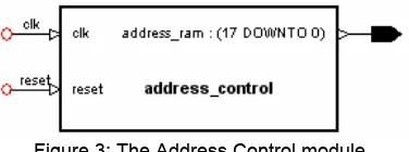
3.3 Address Control module
The function of the address control module is to generate and control addresses of the plaintext and ciphertext words to be read and stored in the memory unit respectively. This module sends the plaintext word address (read address) generated by read counter during read clock cycle. Afterwards, it sends the ciphertext address (write address) generated by write counter during the write clock cycle. The output of this module is 18-bit long because we have used in this design memory of 256 KB. The read counter generates addresses starting from Hx”00000”. The write counter generates addresses starting from location Hx”3FFF9”. The difference between the read address and the write address is 8 positions so that the ciphertext word will be stored in the same position of its plaintext. The conceptual block diagram is shown in Figure 3. The circuit diagram is shown in Figure B.3.
Figure 3: The Address Control module
3.2 The Encryption module
This module performs the encryption operation and it also generates the sub-keys from the original user key. The Encryption module consists of nine components; eight round units (round0 - round7), and the key generation unit. This module accepts plaintext word and user key of 128 bits and generates the cipher word after eight rounds. Each round is completed in one clock cycle. During this round some operations on the input with four sub-keys are carried out. These operations are addition +, xor
⊕
, right rotation >>>, and ordered operation⊗
. Each round from 0 to 6 uses four sub-keys. The last round uses eight sub-keys. The conceptual block diagram is shown in Figure 4. The circuit diagram is shown in Figure B.4.Figure 4: The Encryption Module
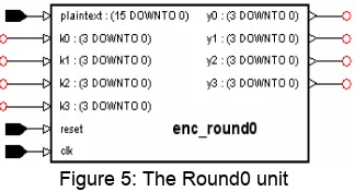
3.2.1 The Round unit
The round unit contains eight rounds (roun0 – round7). The round0 accepts the plaintext word and divide it to four parts (x0, x1, x2 and x3). Subsequently, it applies some operations with four sub-keys as described above. The block diagram of this unit is shown in Figure 5.
Figure 5: The Round0 unit
The four output buses of the enc-round0 are connected to the inputs of the enc-round1. The same connections apply to other units from round1 to round 6. This is achieved by taking four inputs from the next round and connecting them to the four outputs of the previous round as shown in Figure 6.
Figure 6: The Round1-round6 units
The round7 is the last round. It takes the four outputs of round6 as inputs and applies some operations with eight sub-keys. Finally, the four parts of the ciphertext are collected together to produce one cipher word as shown in Figure 7. All rounds have the same architecture; however their functionalities are different depending on the order of the round.
Figure 7: The Round7 unit
3.2.2 The key generation unit
The input to this unit, as shown in Figure 8, is a user key of 128-bit long. When the reset signal takes place, the unit accepts the input user key and generates the sub-keys. These sub-keys are used as inputs to the eight-round units as mentioned above. The circuit diagram is shown in Figure B.5.
Figure 8: The key generation unit
IV. S
IMULATIONAt the start when the reset signal is active, the key generation unit in the encryption module accepts the user key and generates the sub-keys. Then at each clock, the address control module generates an address to the memory unit. The read operation is performed in one clock cycle and the next clock is used for the write operation. During the read operation, one plaintext word arrives to the encryption module from the memory unit through the signal plaintext. The address control unit also produces an address position to store a cipher word at the rising edge of the write clock. Therefore, at every two clock cycles there will be one read operation and one write operation. Figure 9 shows the results of the simulation of the address control module.
Read address Write address Address_ram (one clock for read and one clock for write) Figure 9: Simulation of the address control module
Cipher text word Plain text word User Key ( 128 bits)
Addresses for read and write operations Cipher words stored in memory
Figure 10: Simulation of the encryption module
V. I
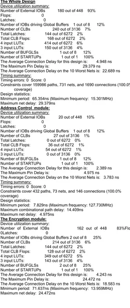
MPLEMENTATIONR
ESULTSWe have used the XC4000XLA Xilinx family to implement our design. We have used this device because the number of Input/Outputs in our design is 180 ports and this family is suitable for this design. Although we understand that there are now Xilinx families with more advanced features, however most of the standard literature on FPGA implementation of encryption algorithms was performed using this family. A comparison with these implementations, using the XC4000 FPGA family, is shown in Appendix A. With the exception of the YAEA implementation, the comparison demonstrates the pre-eminence of the discussed algorithm and our proposed micro-architecture. This is based on the data throughput, the consumed area, and the proposed functional density figure-of-merit. In appendix B we provide a summary of the details of the timing reports. These reports were taken for a 16-bit block plain text, 128 bits key and a cipher text of 16 bits. The details of these reports are as shown in the above-mentioned appendix. Moreover, the design floor plan and the circuit diagrams of all modules are also provided.
VI.
S
UMMARY ANDC
ONCLUSIONThe PYRAMIDS is an iterated cipher consisting of a repeated application of a simple round transformation with different operations and different sequences in each round. The special features of the proposed micro-architecture are summarized as follows:
• A hardware-adapted version of the encryption algorithm “PYRAMIDS” is presented in this work. This adapted version is suitable for FPGA or ASIC-type implementations due to appreciable saving in implementation area, as counted by the number of gates.
• When the round function is changed dynamically, then one can establish that the algorithm output varies for every input user’s key.
• The encryptor part of the micro-architecture can easily be integrated before the router at the sender side. The decryptor, essentially of the same design as the encryptor, is integrated after the router at the receiver side. Thus, one can realize a virtual private network VPN for security-demanding applications. On the other hand, this micro-architecture can be part of a more comprehensive security processor structure.
• As shown in Table A.1 and Figure A.1, the algorithm provides a performance that surpasses the implementations of the RC-6, TWOFISH and SERPENT. The performance metric is based on the functional density figure-of- merit. This performance edge is quite encouraging since the algorithm belongs to the same family of RC algorithms.
Based on the discussed comparison, one can conclude that the micro-architecture performance is satisfactory for packet-level high-security applications of today’s networks.
R
EFERENCES[1] H. Al Hassan, Ph.D. Thesis, Cairo University, in progress, expected 2005.
[2] M. Saeb, A. Zewail, A. Seif, “A Micro-architecture Implementation of YAEA Encryption Algorithm Utilizing VHDL and FPGA Technology,” Third International Conference on Electrical Engineering, ICEENG, Military Technical College, Egypt, 2002.
[3] S. Trimberger, R. Pang, A. Singh, “A 12 Gbps DES Encryptor/Decryptor Core in FPGA,” Lecture Notes on Computer Science, pp. 156-163, Springer-Verlag, 2000.
[4] J. Goodman, A. Chandrakasan, “Energy-Efficient
Reconfigurable Public- Key Cryptography Processor Architecture,” Lecture Notes on Computer Science, pp. 175-190, Springer-Verlag, 2000.
[5] Dandalis, V. K. Prasanna, J.D. P. Rolin, “A Comparative Study of Performance of AES Final Candidates Using FPGAs,” Lecture Notes on Computer Science, pp. 125-140, Springer-Verlag, 2000.
A
PPENDIXA
Comparison with other implementations of well-known algorithms
The following table [2], [3], [4], [5], [6] and the accompanying chart provide a comparison of various algorithm FPGA implementations. We have used a figure-of-merit that is equal to the obtained throughput divided by the area consumed in realizing this architecture. A chart is given below that demonstrates this functional density figure-of-merit for some of the standard algorithms.
Table A.1
A comparison between FPGA implementations of various algorithms Figure of merit for selected algorithms
0
Figure A.1: The Functional Density for our design and some algorithms’ FPGA implementations
APPENDIX B
Implementation reports
In this appendix, we provide the details of the implementation reports as they were made available by FPGA advantage and Xilinx software for HDL design.
Design Information
The Average Connection Delay on the 10 Worst Nets is: 22.689 ns Timing summary:
Timing errors: 0 Score: 0
Constraints cover 159986 paths, 731 nets, and 1690 connections (100.0% coverage)
Design statistics:
Minimum period: 65.354ns (Maximum frequency: 15.301MHz) Maximum net delay: 29.379ns
Address Control module:
The Average Connection Delay on the 10 Worst Nets is: 3.783 ns Timing summary:
Timing errors: 0 Score: 0
Constraints cover 432 paths, 73 nets, and 146 connections (100.0% coverage)
Design statistics:
Minimum period: 7.829ns (Maximum frequency: 127.730MHz) Maximum combinational path delay: 14.409ns
Maximum net delay: 4.975ns
The Encryption module: