Silicon photonic crystal nanocavity
modulator and receiver fabricated by
photolithography
February 2019
A thesis submitted in partial fulfilment of the requirements for the degree of Doctor of
Philosophy in Engineering
Keio University
Graduate School of Science and Technology
School of Integrated Design Engineering
ABSTRACT
i
Abstract
Silicon (Si) photonics is considered a promising candidate as a key technology with which to develop optical interconnects due to the mature state of nanofabrication, together with the unique characteristics of Si, namely a high refractive index and a low absorption loss at telecom wavelengths, thus offering the advantage of confining light in a tiny device on a chip. Today, researchers are working towards accomplishing complementary metal-oxide-semiconductor (CMOS) compatible fabrication, which will allow Si photonic devices to be commercialized.
On the other hand, Si photonic crystal (PhC) has been attracting a lot of attention since it enables us to device high-Q nanocavities with small mode volume. This feature has facilitated various functional operations at a very low power. Hence, the integration of a Si PhC with Si photonics will allow us to expand the functionality of Si photonic systems. Although it is often claimed that existing Si PhC devices are compatible with CMOS and Si photonics, several challenges need to be met before integration is achieved.
This thesis discusses the fabrication of CMOS compatible high-Q Si PhC nanocavities and studies the functionality of these devices. CMOS compatible fabrication allows the device to be easily integrated with heaters and p-i-n diode structures, and this enables us to demonstrate integrated optical modulator and receiver operation at a very low power.
Chapter 1 describes the background and the motivation of this study. It reviews the current Si photonics and Si PhC technologies.
Chapter 2 presents the theory. It describes the principle of photonic bandgap and the formation of nanocavity in a PhC. The design strategy for achieving a high-Q PhC nanocavity is described.
Chapter 3 presents the fabrication process of the PhC device with the integration of a p-i-n
diode structure. A very high Q of 2.2×10⁵ is achieved with a p-i-n integrated Si PhC nanocavity
ABSTRACT
ii
Chapter 4 reports the demonstration of a PhC nanocavity device as an electro-optic modulator by injecting a carrier into a p-i-n diode. Refractive index modulation is demonstrated via the carrier plasma dispersion effect, with modulation voltage of 1.0 V at a speed of 0.35 GHz.
Chapter 5 reports the demonstration of a PhC nanocavity device as a photoreceiver with the help of two-photon absorption. A small dark current of38 pA with a minimum detectable power of10 µWis obtained.
Chapter 6 describes a transmittance experiment using a Si PhC nanocavity modulator and receiver. This demonstration shows that an all-silicon transmission link is achievable.
LIST OF ABBREVIATIONS iii
List of abbreviations
1D One dimensional 2D Two dimensional 3D Three dimensional AC Accumulative current Al Aluminium BPF Band-pass filterCMOS Complementary metal-oxide-semiconductor
CW Continuous wave
DC Direct current
EB Electron beam
EDFA Erbium-doped fiber amplifiers
EO Electro-optic
FDTD Finite difference time domain
FWHM Full width at half maximum
GaAs Gallium arsenide
Ge Germanium
InP Indium phosphate
IR Infra-red
MZI Mach-Zehnder Interferometer
NRZ Non-return zero OE Opto-electric OSC Oscilloscope PBG Photonic bandgap PD Photo detector PhC Photonic crystal PM Power meter
LIST OF ABBREVIATIONS
iv
PRBS Pseudo-random bit sequence
PW Plane wave
RF Radio frequency
Rx Receiver
SEM Scanning electron microscopic
Si Silicon
SiO2 Silica
TE Transverse electric
TEC Thermoelectric temperature controller
TIA Transimpedance amplifier
TIR Total internal reflection
TLD Tunable laser diode
TM Transverse mode
TO Thermo-optic
TPA Two-photon absorption
Tx Transmitter
VOA Variable optical attenuator
CONTENTS
Contents
Abstract
... i
List of abbreviations ... iii
Chapter 1 Introduction ... 1
1.1 Integrated Silicon Photonics and data centers ... 2
1.2 Photonic crystal ... 4
1.2.1 One-dimensional PhC ... 5
1.2.2 Two-dimensional PhC ... 6
1.2.3 Three-dimensional PhC ... 10
1.3 Optical signal processing ... 12
1.3.1 Electro-optic modulator ... 12
1.3.2 Photoreceiver ... 14
1.3.3 Optical transmission link ... 16
1.4 Purpose of Study ... 18
1.4.1 Motivation ... 18
1.4.2 Objective ... 19
Chapter 2 Theory of Photonic Crystal ... 21
2.1 Introduction ... 21
2.2 Photonic band structure ... 22
2.2.1 Maxwell’s equation ... 22
2.2.2 Cavity formation ... 27
2.3 Fabry-Pérot Cavity ... 30
2.4 Method of analysis ... 32
2.4.1 Plane-wave (PW) method ... 32
2.4.2 Finite difference time domain (FDTD) method ... 37
2.5 PhC nanocavity design structure ... 40
2.6 Summary ... 43
Chapter 3 PhC nanocavity laterally embedded with p-i-n diode fabrication
process ... 44
3.1 Introduction ... 44
3.2 Overview of PhC fabrication process ... 45
3.3 Photolithography fabrication procedure ... 46
3.3.1 Device fabrication process ... 46
CONTENTS
3.4 Comparison with previous study’s device... 51
3.5 Summary ... 52
Chapter 4 Electro-optic modulator based on PhC nanocavity ... 53
4.1 Introduction ... 53
4.2 Motivation ... 54
4.3 Spectrum characteristics ... 55
4.3.1 DC voltage operation ... 56
4.3.2 Radio-frequency (RF) operation ... 59
4.4 Electro-optic (EO) modulations ... 61
4.5 Discussion ... 62
4.6 Summary ... 64
Chapter 5 PhC nanocavity photoreceiver ... 65
5.1 Introduction ... 65
5.2 Motivation ... 66
5.3 Photoreceiver properties ... 67
5.3.1 Dark current... 67
5.3.2 Transmission spectrum and photocurrent ... 68
5.3.3 Responsivity ... 69
5.4 Photoreceiver operation ... 70
5.5 Discussion ... 72
5.6 Summary ... 74
Chapter 6 All-Si scheme PhC nanocavity transmission link ... 75
6.1 Introduction ... 75
6.2 Challenges and motivation ... 76
6.3 Electro-optic modulator performance ... 77
6.4 Opto-electric receiver performance ... 78
6.4.1 Basic design structure ... 78
6.4.2 Design characteristics ... 80
6.4.3 Demonstration of OE receiver ... 81
6.5 Temperature dependence operation... 82
6.6 All-Si scheme PhC transmission link demonstration ... 84
6.7 Discussion ... 85
6.8 Summary ... 86
Chapter 7 Summary and outlook ... 87
CONTENTS
7.1.1 Theory of photonic crystal (Chapter 2) ... 87
7.1.2 PhC nanocavity laterally embedded with p-i-n diode fabrication process (Chapter 3) ... 88
7.1.3 Electro-optic modulator based on PhC nanocavity (Chapter 4) ... 88
7.1.4 PhC nanocavity photoreceiver (Chapter 5) ... 89
7.1.5 All-Si scheme PhC nanocavity transmission link (Chapter 6) ... 89
7.2 Conclusion and outlook of the thesis ... 89
References ... 92
Acknowledgments ... 106
List of publications ... 108
Appendix A Product values of optical equipment’s ... 111
CHAPTER 1. INTRODUCTION
1
Chapter 1
Introduction
The use of light for communication purposes has begins in early years of civilization. Reflection of light through mirrors, fire beacons or smoke signal are used to convey an information at some distance. For example, in 1084 B.C., Greeks civilization constructed a 500 km long line fire beacons to convey news of victory [1]. Through years, researchers are trying to manipulate light as medium of communication to carry information signals at distance due to its fast speed. Only in 1966, with the advancement of technology, low-losses optical fibers has been invented and become the best choice for optical communication. Since fibers are capable of guiding light in similar confinement of electrons inside copper wire, optical communication has become widely used in telecommunication technology.
Nowadays, telecommunications network has expanded the entire world. Transmitting an information signal no longer required a long time. Signal can be received within a minute although it was transmitted over a far distance. Therefore, previous decades have witnessed an explosive increasement in the volume of global network. In 2015, amount of annual global data center traffic already reached 1021 bytes and estimated to be triple by 2020 [2]. Data intensive applications such as streaming video, social network and cloud computing require data center to provide extremely high bandwidth communication. Transporting such increasing volume of data with existing technologies such as the conventional metallic interconnects, will not able to satisfy the exponentially increasing capacity demands. This is because the conventional interconnects are limited by the finite resistance and capacitance, soon will reached its limit [3]. Meanwhile, the scale expansion of data center will consume huge power. Therefore, efficient interconnection scheme with low cost, high energy efficiency and high bandwidth capacity is in a great need.
CHAPTER 1. INTRODUCTION
2 Currently, present work is concerned with monolithically integrated optics on a silicon platform, for example, silicon photonics. Fuelled by modern society’s consumption of digital electronics, silicon manufacturing technology nowadays represent an extremely mature process that has had half a century of continuous, law-like [3], exponential improvements and breakthroughs.
Photonic crystal, on the other hand, is a material where the refractive index change periodically [4], may hold the key to continue the progress towards all-optical integrated circuits. Photonic crystal is characterized by the formation of band structures with respect to energy of photon. Thus, various type of engineering focusing on band gap, band edge and photons manipulation has been investigated to broad the application of photonic crystal to optical chip and functional devices.
In this chapter, the integration of silicon photonics with electronics will be discussed in detail. Next, the introduction about photonic crystal and their characteristics will also be explained in this chapter. Then, a few examples of optical signal processing will be introduced. Finally, the purpose of this study is described.
1.1
Integrated Silicon Photonics and data centers
Nowadays, data rates have becoming a great attention in order to achieve high transmission signals. According to Moore’s Law, electronic transmission is facing a breaking point when the ability of copper wire has come to its limit. Fig. 1.1 illustrates the numbers of transistors on a chip as a function of year. The trend shows the number of transistors is increasing over year. Thus, more power is needed to carry data in high speed over a long distance. Therefore, scientist introduced the integrated photonics to transform communication industry expecting to downsizing the size, mitigate the fabrication cost and achieve better performance.
Fig. 1.1 Number of transistors as a function of time based on different processor’s company. Black, red, green and blue refer to Intel, IBM, AMD and Acorn/DEC/Apple, respectively. [https://en.wikipedia.org/wiki/Transistor_count] 1970 1980 1990 2000 2010 2020 103 104 105 106 107 108 109 1010 1011 Intel IBM AMD Acorn/DEC/Apple Transistor count Year
CHAPTER 1. INTRODUCTION
3 Instead of utilizing electrons, integrated photonics use light. It is possible to perform in wide variety application involving optical functions. The dimension of integrated photonics has been expanded due to the recent development in nanostructures and silicon technologies. This has led to the transformation in optical devices field technologies for many applications including optical networks, optical interconnects, lab on chip etc. Silicon photonic has been targeted at applications in intra-chip and inter-chip optical interconnects. It is expected to solve the bottlenecks of metal electrical interconnects at high data rates by delivering optical connectivity everywhere from the network level to chip-to-chip level.
Present work on silicon photonics focuses in data center networks. In a sense, data centers are at the core of the internet, with virtually all internet traffic ending up in data center server. With the massive popularization, within the last decade, of cloud computing, cloud storage, streaming media and mobile computing devices, data center traffic has growth rapidly. By 2015, the number of networked devices equal to two times of the global population. The number is expected to rise more with the increasing of years. Such massive growth will become a challenge for future scalability and lead to network congestion. Therefore, to help combat the rapid growth in the bandwidth demand of data center networks, all-optical networking technology is introduced, for rack-to-rack and board-to-board communications, to replace bandwidth-limiting electronic components.
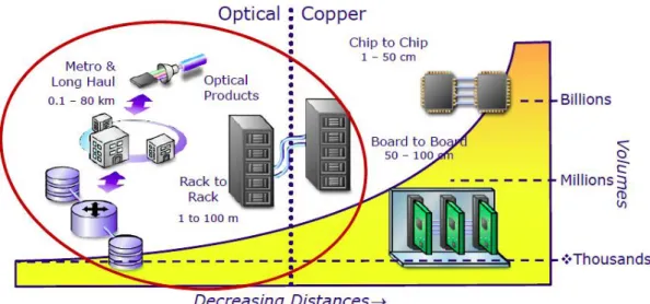
Fig. 1.2 Battle between optics and copper.
However, future data center networks are expected to scale to millions nodes [5], [6], which will require compact, energy efficient and easily manufacturable components. This poses a problem for conventional off-the-shelf optical components, which are bulky, consume many watts of power and relatively expensive to manufacture. Therefore, silicon photonics which relatively inexpensively in term of manufacture due to wafer-scale processing, becomes an obvious candidate for use in future data center networks.
CHAPTER 1. INTRODUCTION
4 Fig. 1.3 Development of optics in data center since 90’s.
1.2
Photonic crystal
Photonic crystal (PhC) is a periodic dielectric structure. PhC exist in nature, for example wings of butterfly and it also can be artificially fabricated. Although scientist from America, Yablonovitch, has become the pioneer in PhC when he claimed that spontaneous emission can be controlled through electromagnetic band gap of periodic dielectric structure [4], the study of the periodic structure has been started hundred year ago by Lord Rayleigh [7]. Rayleigh discover that band gap can be achieved in one-dimension periodic structure. However, in early year, this phenomenon was ignored by the photonics community. Then, S. John reported that Anderson localization of photon can be achieved by including certain amount of disorder in superlattice structure [8]. At that period, name of ‘photonic crystal’ has not been introduced yet until Yablonovitch and Sajeev met each other [9].
The advantage of PhC structure is not only lies on the ability to manipulate light or photon but also the miniaturization of the structure due to the small mode volume. Together with the developing fabrication technologies, it is possible to fabricate such compact PhC devices. The direction of application of PhC devices currently is towards communications filed since photons are excellent in transmitting information. Various devices of optical interconnect have been introduced and demonstrated by all PhC structures.
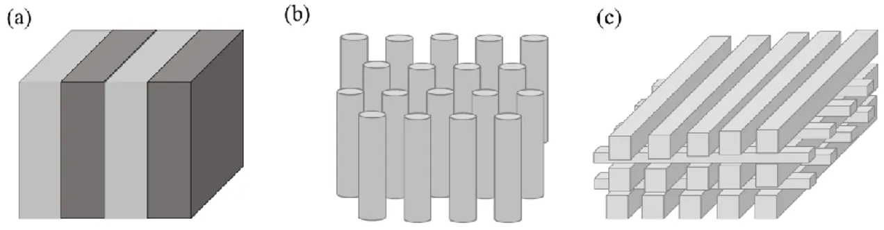
PhC structure can be formed in three different dimensions as shown in Fig. 1.4. Each dimension has different structure and application. The structure and application will be discussed in following section.
CHAPTER 1. INTRODUCTION
5 Fig. 1.4 Schematic illustration of PhC structures (a) one-dimensional (1D) (b) two-dimensional
(2D) (c) three-dimensional (3D)
1.2.1
One-dimensional PhC
One-dimensional (1D) PhC nanocavity has a simplest structure in PhC as shown in Fig. 1.4 (a). The investigation of 1D PhC structure has been done by L. Rayleigh in 1887 [7]. Compared with 2D and 3D PhC, 1D PhC easy to integrate with other existing photonic devices due to the simple structure without changing fabrication procedures. 1D PhC structure mainly used in grating couplers. Grating couplers is a device that can diffract light from propagation in the waveguide to free space. By placing an optical fiber above the chip, part of the radiated light is collected. Usually grating coupler is used as an I/O device to couple light between fiber and sub-micrometer silicon waveguides. It can be placed anywhere on the surface of the chip to enable input and outputs. Fig. 1.5 shows an illustrated of cross section view of grating coupler. The thickness of the buried oxide layer is determined by the wafer type. The study of grating coupler was first proposed in 1970 [10]. In this paper, the method of coupling light into a thin-film optical waveguide using a grating coupler was first introduced. Then, study and application of grating coupler begin to expand extensively [11]–[15].
Fig. 1.5 Schematic illustration of cross section view grating coupler. The thickness, h is normally 150– 300nm. The cladding material is usually air (n2 = 1), silicon dioxide or
index-matching liquid (n2 ~ 1.45)
Another usual application of 1D PhC structure is nanobeam structure. A feasible nanobeam structure operate at 1.55 µm wavelength was first fabricated in 1995 [16] and first reported experimental Q factor of this structure was 265 [17]. Q factor is a measured value to evaluate the ability of light confinement in a designed structure. The investigation of design,
CHAPTER 1. INTRODUCTION
6 fabrication and experimental characterization of PhC nanobeam then continue to improve the value of Q. On 2009, Q of 105 has been reported by Loncar’s group [18] and later, the same group
have reported with an optimized of nanobeam structure is possible to achieved a theoretical highest Q of >109 [19].
Fig. 1.6 (a) Schematic illustration of PhC waveguide microcavity with dimension for operation at 1.54 µm.The parameter of hole period, a, defect length, ad, hole radius, r, waveguide
width, w, silicon thickness, tSi, and total etch depth through both Si and SiO2 are described.
(b) Computation and transmission through the structure. Resonance appeared at 1547 nm with Q of 280. [Reprinted with permission J.S. Foresi et al., Nature 390, 1997] (c) and (d) Electric field (Ey) profiles of two cavity modes. Q and V are quoted for the optimal
cavity length, s. (e) SEM image of fabricated PhC nanobeam cavity with 220 nm thickness and 500 nm width. The photonic mirror pitch a=430 nm is linearly tapered over five hole section to a= 330 nm at the cavity center. The hole radius is r = 0.28a and the band gap extends from 1200-1700 nm. [Reprinted with permission P. B. Deotare et al., Appl. Phys. Lett. 94 (121106), 2009]
Although the development of 1D PhC structures later compared to two-dimensional PhC structure, due to the extraordinary ability where it allows refractive index distribution along one direction and localization of light in a small region area, makes this structure compact. Owing to the compactness, it has widely used for wide range of application with high performance [20]– [23].
1.2.2
Two-dimensional PhC
Two-dimensional (2D) PhC structure, has become more dominant in PhC structures due to the possesses periodicity of the permittivity along two-direction. Because of that, it is possible to have large variety of configuration. The study of 2D photonic band structures was first theoretically conducted by M. Plihal, who is investigating the electromagnetic waves of photonic band structure that consists of long, parallel and dielectric rods of periodic array constitute a square lattice [24] and on the same year, the same method was conducted to calculate for a
CHAPTER 1. INTRODUCTION
7 triangular lattice [25]. Later the demonstration of microwave transmission was performed to verify that light could not propagate in the 2D complete band gap structure at any polarization [26].
Since the application of 2D PhC structures are depending on the ability to control and confine light, several methods has been introduced to manipulate photons in the structure which is 1) band-gap nanocavity and 2) mode-gap nanocavity.
1) Band-gap nanocavity occurs when defect is introduced within a photonic band gap and light is confined with surrounding band-gap. This strategy has been introduced by Yablonovitch to form a high Q through donor and acceptor modes concept in 3D periodic dielectric structure [27]. Then, few years later, the donor and acceptor modes strategy has been utilized in 2D microfabricated hexagonal array PhC structure theoretically and experimentally [28], [29]. The light confinement occurs through the presence of defect by removing a single hole as shown in Fig. 1.7. Due to the total internal reflection, photons are localized vertically at the slab interface. 3D confined optical mode was achieved because of the combination of Bragg reflection from 2D PhC and total internal reflection from the low index cladding of air. The value of Q experimentally measured was 250, however, by tailoring the interhole spacing and radius holes, value of Q can be further improved to 1500. The structure has been demonstrated as microcavity laser and pulsed lasing action was observed at 1.5 µm wavelength.
Fig. 1.7 (a) SEM image of top view of a microfabricated 2D hexagonal array of air holes in a thin membrane with a missing hole at the center. The interhole spacing, a is 515 nm and the radius holes, r is ~180 nm. The two enlarged holes which radius, r’ of 240 nm, are used to split the dipole mode degeneracy. (b) Cross section through the middle of the PhC microcavity. A defect is formed by removing a single hole. [Reprinted with permission O. Painter et al., Science 284, 1999]
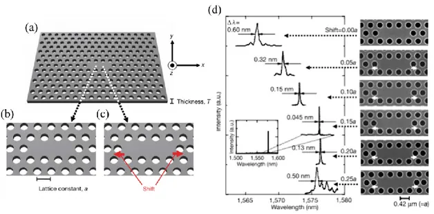
Then, the value of Q is further improved by the introduction of L3 nanocavity by Noda’s group [30]. The structure consists of three missing air holes in a line at the center as shown in Fig. 1.8 (a) of the structure so that Bragg reflection at the in-plane direction occur and light can be confined. In order to obtain high Q, they have modified the Bragg reflection condition by shifting the air holes at both cavity edge 0.15a from original position. The theory is, by the shifting of air holes position, changed the phase of partial reflections at the air holes, and thus, the phase mismatch occur which will weaken the Bragg reflection. Light then will penetrate more inside the mirror
CHAPTER 1. INTRODUCTION
8 and will reflected perfectly. Fig. 1.8 (b) shows the experiment results of various air holes distance shift and their corresponding spectrum. The highest value of Q was 45000 was obtained when the air holes was shifted by 0.15a. Thereafter, the tuning was performed not only adjacently to the nanocavity but also for those two and three points away [31] where the Q was improved to 100000. With the high Q obtained, the application of such device was studied. All-optical switching devices [32]–[34] and semiconductor laser [35] has been demonstrated.
Fig. 1.8 (a) Schematic of cavity structure of triangular lattice air holes with lattice constant, a is 0.42 µm, thickness, T of 0.25 µm and radius R of 0.12 µm. (b) Cavity structure with three missing air holes in a line. (c) Method of enlarging the Q of a donor-type defect by displacing the air holes at both edges. (d) SEM image of a nanocavity with various shifting distance and corresponding resonance spectrum. [Reprinted with permission Y. Akahane et al., Nature 425, 2003]
2) Mode-gap nanocavity is formed with different lattice constant or width of waveguide in PhC structure. Noda’s group has introduced a mode-gap nanocavity by triangular lattice double heterostructure nanocavity as shown in Fig. 1.9 [36]. The structure consists of missing row of air holes which formed a waveguide that allows propagation of photons and PhC with two different lattice constants, a1 and a2 are introduced to the structure (I and II) to differ the transmission and
mode-gap regions. Therefore, only photons with specific energy can exist in the PhC waveguide II and with the short length of waveguide in PhC II will limit the frequency of photons exists in the region and nanocavity was formed. The difference of lattice constant between PhC I and II gives a mode-gap effect. Therefore, by changing the difference of lattice-constant between two crystals, can controlled the evanescent behaviour of electric field confined. The structures achieved high Q of 600000 through experiment and theoretically 20000000 with the optimization structure.
CHAPTER 1. INTRODUCTION
9 Fig. 1.9 (a) 2D PhC slab of triangular lattice structure with line-defect waveguide formed by a missing row of air holes. (b) The calculated band structure for (a). The blue arrow indicates the transmission region where the propagation of photons is allowed through the waveguide and the red arrow indicates the mode-gap region in which the propagation is inhibited. (c) Photonic double heterostructures, constructed by connecting the basic PhC structures I and II. PhC I have a triangular lattice structure with lattice constant of a1
while PhC II has a deformed triangular lattice structure with a face-centered rectangular lattice of constant a2 (>a1) in the waveguide direction; it retains the same constant as PhC
I in the orthogonal direction to satisfy the lattice-matching conditions. (d) Schematic of the band diagram along the waveguide direction. Photons of a specific energy can exist only in the waveguide of PhC II. [Reprinted with permission B.S Song et al., Nat. Mater.
4, 2005]
Another structure of mode-gap nanocavity which has been introduced is width modulated line-defect cavity [37]. The cavity structure was created by modulating the holes parameter of line-defect waveguide to create local confinement as shown in Fig. 1.10 (a). The mode-gap in this cavity is realized by the difference of waveguide width once the holes parameter is modulated. The band diagram of the structure as shown in Fig. 1.10 (b) shows that the difference in the cut-off frequency of TE mode, between W0.98 waveguide and the cavity allow light to be confine. This structure allows local light modulation with small number of shifting holes that gives a great advantage to the cross-packed integration of PhC slab device. The study able to achieve value of
Q factor 105.
This nanocavity structure has been demonstrated as an all-optical switching in which consumed low energy consumption and fast all-optical switching [38], [39]. With the unique properties of PhC structure and together with the advancement of the fabrication technologies nowadays, researchers are now move towards the integration of PhC devices with CMOS electrical circuits.
CHAPTER 1. INTRODUCTION
10 Fig. 1.10 (a) Schematic illustration of width-modulated line defect PhC nanocavity. The center airholes was shifted to some position from their original position. d is the number of barrier region that set the strength of coupling and confinement. (b) Band diagram dispersion of the line defect with SiO2 cladding. The solid red line represents the
dispersion of the barrier W 0.98 waveguides without cavity and the dashed line represents when the waveguide width is 18 nm wider with cavity hole shifts.
1.2.3
Three-dimensional PhC
In 3D structure, photonic band gap formed in all direction. Therefore, a complete photonic band gap is formed with 3D PhC structure. The schematic of 3D PhC structures shown in Fig. 1.4(c). The photonic band structure of 3D PhC has first introduced by Yablonovitch [40]. He has proven that full 3D photonic band gap is achievable in some type of dielectric structure and the forbidden gap can be created in microstructures which agrees to practical microfabrication. Many works are donated to the design of new geometric configuration of 3D PhC, which open new possibilities of applications. Stone opal is one of the famous naturally formed of 3D PhC which has a unique optical property as shown in Fig. 1.11. Different colour will appear when the stone is turned around in which ancient people believe the stone opal have a magic power. It is consisting of a number of microspheres placed at nodes of face-centered cubic lattice where reflectance is depending on the radiation angle.
Similarly, with 1D and 2D PhC structure, 3D PhC structure also has an ability of light confinement. Recently, high Q factor was reported to achieve 93,000 [41] as shown in Fig.1.12. The high Q factor is expected to achieve less threshold less lasing oscillation for 3D light confinement. Although 3D PhC structure is an ideal structure due to the complete photonic band gap characteristics, the fabrication of the structures is difficult compared to 2D and 1D PhC. So far, there is no reliable technology to fabricate this structure at optical telecommunication wavelength. Therefore, most of 3D PhC focus on fabrication method [42], [43].
CHAPTER 1. INTRODUCTION
11 Fig. 1.11 Image of stone opal which has unique optical property. The colour of the stone will
change when the stone is turned around. [https://www.gia.edu/opal]
Fig. 1.12 (a) SEM image of stacked sample having 16 lower plates, single active plate and 16 upper plate. (b) Photoluminescence spectrum around 1231 nm for an input power of 4.35 µW, which is below threshold power of 4.59 µW. Red curved shows the fitting to evaluate the Q factor. (c) Experimentally and numerically obtained Q factor of upper plates. [Reprinted with permission S. Takahashi et al., Electronics Letters 54 (5), 2018]
CHAPTER 1. INTRODUCTION
12
1.3
Optical signal processing
Optical signal is an optical communication that utilizing light to transmit the signal instead of electrical current and signal processing is a process to analysis, synthesis and conversion of signal. So, optical signal processing is a process that utilize light to analyse and make a modulation of signal before the signal is received to the receiver. Nonlinear devices, analog and digital signals and advanced data modulations are the examples of optical signal processing fields that has been extensively study among the researchers. In this section, some of the basic optical devices is discussed – namely, electro-optic modulator and photoreceiver – to bridge the electrical circuit with photonics through electro-optic and opto-electronic conversion. Next, the combination of the transmitter and receiver in a single housing is discussed.
1.3.1
Electro-optic modulator
Electro-optic modulator (EOM) is one of main material for optical interconnect. It modulates (makes the fundamental characteristics become vary) a light beam propagating either in free space or in an optical waveguide. An optical modulator can alter different beam parameters, allowing them to be categorized as either amplitude, phase or polarization modulators. There are two types of modulator namely, electro-absorptive modulator and electro-refractive modulator. Electro-refractive modulator works when electric field is applied to the material and changed its real part of refractive index. A change of refractive index in the imaginary part is known as electro-absorptive modulator. In semiconductor material, Pockels’ effect and Kerr effect are mainly the electric field effects that usually caused electro-refractive or electro-absorptive. However, in pure silicon telecommunication wavelength, Pockels’ and Kerr effect are weak [44]. Hence, other approach is necessary for the realization of silicon modulation.
In early years, lithium niobite (LiNbO3) modulator has been proposed due to the fact that
it possesses a large electro-optic coefficient [45], enabling optical modulation via Pockels’ effect. In 1973, thin-film LiNbO3 electro-optic light modulator with maximum bandwidth of 3.2 GHz
has been proposed [46]. Then, the bandwidth performance has been improved and currently, LiNbO3 modulator has become commercialized [47]–[50]. Although performance of LiNbO3 has
been improved, the device still suffers for a large foot-print thus, which led to high power consumption.
The dominance of Si as semiconductor, eventually led to the investigation of Si photonic circuits. This is because, Si material has potential attraction of integration with electronics in a cost-effective manner. In addition, since silicon modulation is possible to achieve by the changes of refractive index as experimentally proven by Soref [44], researchers are towards silicon-based material of modulator due to the unique properties of silicon. In 1987, Si has been proven for guided-wave modulator and switches applications because its ability to exhibits electro-refraction effects and free-carrier dispersion effect [51]. Since then, research regarding Si modulator become vigorously among researchers.
However, in early years, silicon waveguide based optical modulator was generally slow. However, early 2000s, performance of optical modulator has been optimized and reported possible to operate at high-speed operation of MHz and GHz [52]. In 2012, Mach-Zehnder Interferometer (MZI)-based modulator which operate via carrier depletion technique has obtained a highest bandwidth of 50Gbit/s [53]. Carrier depletion technique manipulated free-carrier
CHAPTER 1. INTRODUCTION
13 densities in a modulator to avoid speed limitation posed by minority carrier lifetime. Device that employ this technique usually operates at reverse bias voltage. Another technique is carrier-accumulation which has been demonstrated using MZI-based modulator [54]. It has reported the operating bandwidth of the device is at 10 Gbit/s.
MZI-based silicon modulator has proven to achieve a high operating bandwidth. Although MZI-based modulator has shorter device length compared to LiNbO3modulator, but
still much shorter devices are desired. Therefore, resonant-based modulator is introduced. The resonant-based modulator usually small and compact in size. Therefore, resonant-based structure modulator is expected possible to reduce power consumption of the device. Active high-speed ring resonators were first introduced by Xu et al. in 2005 [55]. A carrier injection scheme is employed and 1.5Gbit/s initial data rate is achieved. Then, carrier-depletion technique is employed to further enhance the modulation [56].
Although significant foot-print can be reduced with resonant-based structure, this kind of modulator has a narrowband application due to the narrow modulation range of resonance wavelength. This, however, could limit their application.
Since PhC possible for large-scale integrated optics, and its ability to achieve slow group light velocity, PhC-based MZI modulator has been demonstrated [57]–[60]. On the other hand, PhC-based on resonant structure also has been demonstrated [61].
The performance of EOM device based on its modulation speed and depth, optical bandwidth, insertion loss, footprint and power consumption. However, those metrics of performance involve trade-off. For example, MZI-based modulator, is suffer from the large dimension although it shows a good performance at higher operation bandwidth. If we are towards reducing the dimension, it will be reducing the modulation depth. For ring resonator, in order to increase the optical bandwidth, cascading multiple ring is necessary, as a result it will increase the footprint and complexity in fabrication. Therefore, the performance of modulator is optimized based on its application. In case of sensing application, only moderate modulation speed is required. Fig. 1.13 shows the development of electro-optic modulator by comparing their performance.
CHAPTER 1. INTRODUCTION
14 Fig. 1.13Development of electro-optic modulator by comparing their performance between speed,
size and power consumption.
1.3.2
Photoreceiver
Photoreceiver also known as photodetector or photosensor where it used to sense light or electromagnetic radiation and converts into electrical signal. The operation of light conversion is also known as opto-electronic (OE) operation. In early years, the optical detectors are evolved in III-IV semiconductor compound due to the wide detection ability of wavelength [62]. It also shows an ability for higher speed detection operation due to the high absorption coefficient characteristics.
With the invention of integrated circuit and CMOS technology, optical devices that has a higher degree of integration and compatible with CMOS process has become a trend. In particular, the realization of high-performance silicon-based photodetector becomes a great interest among researchers [63].
Silicon photodiodes are excellent detectors at visible wavelengths, but the development of Si photodetectors operating at wavelengths of interest for telecom and datacom is not straightforward, as Si is transparent at wavelengths larger than 1.1 µm. Conventional Si-based photodetectors at telecom wavelengths utilize integration with other material systems such as III-V compound semiconductors (InGaAs, InGaAsP, InGaAlAs, etc. [64]–[66]) and Ge. However, the 8.1% lattice mismatch between InGaAs and Si makes monolithic integration with CMOS circuit difficult, so a hybrid integration approach is required.
CHAPTER 1. INTRODUCTION
15 Ge on Si photodetectors, requires growth of Ge on a Si substrate. It can operate up until 10 Gbs-1 with high responsivity. However, the devices suffer for high leak current (~ 500 nA)
[67], [68]. However, recently, J. Cui et al. has enhanced the performance of Ge on Si photodetector with optimized DBR location where the dark current can be far reduced as low as 7 nA at 1550 nm operation wavelength [69]. A limitation of Ge-based photodetector is both their incompatibility with an unmodified CMOS process flow and the requirement for a buffer layer that causes problems in both thermal budget and planarity [70].
Another method is defect mediated state photodetector. Defect is introduced into the photodetector to enhance the photon absorption. Defect can be introduced through various method. One of the method is by hyper doping implantation of chalcogens (S, Se, Te) to increase doping concentration of the photodiode [71], [72]. Another way to introduce defect is by implantation of ions [73], [74]. However, this method introduces shallow impurity levels within the Si band gap. Therefore, to overcome this matter, Si+ ion-implantation is proposed. This method allows the
device to all-Si without any integration of other impurities material [75]–[77]. However, similarly, with the Ge integration, ion-implantation method also requires complexity of fabrication. In addition, the presence of defect during the fabrication process will caused an increasement in leak current value. On the other hand, two-photon absorption (TPA) has been reported to achieve all-Si photoreceiver [78], [79] and reported to achieve a minimum leak current (~pA). TPA is a nonlinear optical process where in semiconductor, an electron can be moved into an excited state by the simultaneous absorption of two photons of identical wavelength. TPA allows carriers to be absorbed and allow the generation of photocurrents.
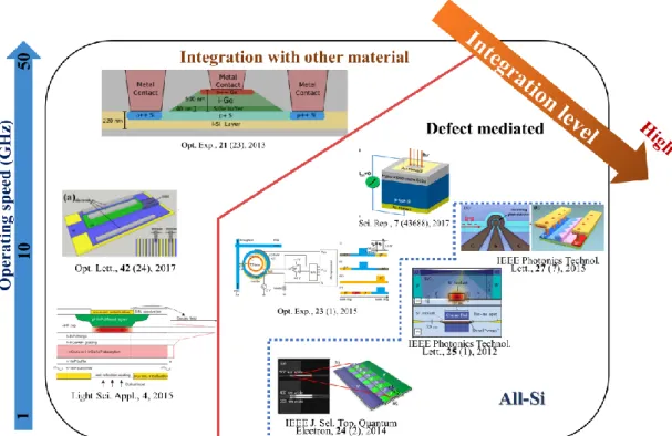
Nowadays, performance of photoreceiver is not only based on operating speed, responsivity and signal-to-noise-ratio, but most importantly based on foot-print, cost of fabrication and ease integration. This is because current silicon optical interconnect is now towards the integration of chip-to-chip or on chip level. Therefore, higher degree level of integration is required. As shown in Fig. 1.14, although integration with other material of photodetectors shows much higher of operating speed, however, all-Si photodetector shows higher degree of integration.
CHAPTER 1. INTRODUCTION
16 Fig. 1.14 Comparison of photodetector performance between integration with other material and
defect mediated.
1.3.3
Optical transmission link
Transmission link system transmits data signal from transmitter to receiver. The system link requires transmitter and receiver to complete the whole signal transmission. The beginning of transceiver introduction was early 1920s where it has been implemented in radio to transmit the electrical wave signal. Then in 1970s, mobile phone has become a complete unit of signal transmission link system. Later, with the increasement of data rates for all interconnects, copper wire in electrical signal has come to its limitations. Researchers proposed that optical data transmission will become the best candidates to overcome this matter due to the ability to carry signal on a single fiber from a few gigabits per second to over one terabit per second.
Fig. 1.15Intel silicon photonics optical transmitter. [Reprinted with permission from Intel brochure.[https://www.intel.com/content/www/us/en/architecture-and
CHAPTER 1. INTRODUCTION
17 First fully integrated optical transmission system in silicon has been demonstrated by Luxtera Inc. [80] and achieved 20 Gbs-1 optical transmission using combination of LiNbO
3
modulator and InGaAsP detector. However, besides large die dimension of the device, power consumption of the system is as large as 2.5 W. Next, the silicon optical transmission system has been commercialized by Intel Silicon Photonics groups. Research regarding Si optical transmission system has been further studied whose low power operation monolithically transceiver has been demonstrated using high-speed MZI modulators [81] by the same group. A year later, compact and even low power consumption monolithic link has been reported [82], [83]. Those devices are the combination of ring-resonator based modulator as transmitter and Ge detectors as receivers.
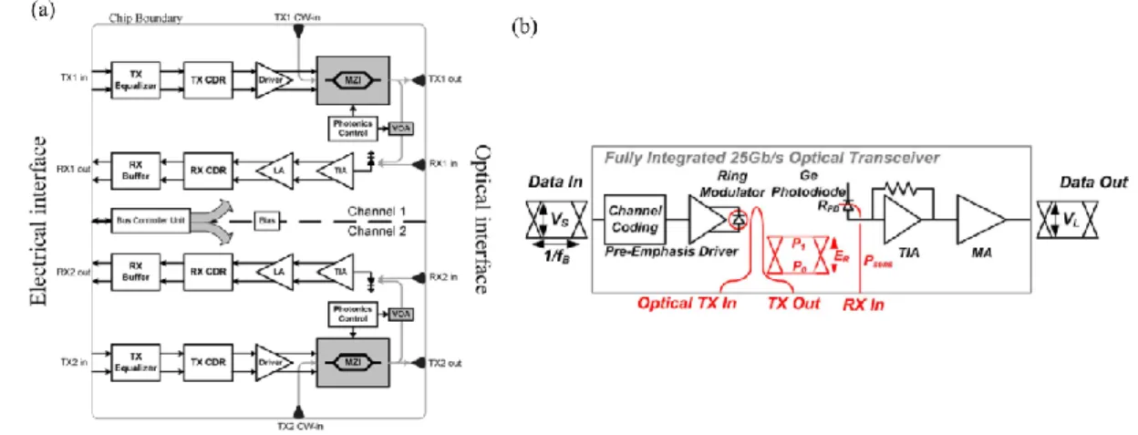
Fig. 1.16 Block diagram of optical transmission device. (a) Dual-channel 10 Gbs-1 transceiver
MZI. [Reprinted with permission B. Analui, et al., IEEE J. Solid-State Circuits 41 (12), 2006] (b) Fully integrated 25 Gbs-1 Si photonic interconnect. [Reprinted with permission
J. F. Buckwalter, et al., IEEE J. Solid-State Circuits 47 (6), 2012]
Due to plasma dispersion effect, silicon has become an excellent material for modulation. Due to that, researchers are utilizing Si-based optical modulator in optical transmission link system [82]–[84]. However, due to the transparency of Si at telecom wavelength, integration with other material of photoreceiver has been utilize in optical transmission link system. Most of the utilizing epitaxially grown Ge or heterogeneously bonded III-V photodetectors at the receiver. Although the combination of Si-based modulator and hybrid photodetector shows a significantly high operating bandwidth, it will become inadequately efficient in future optical transmission link device. This is because, those combination has a lower degree of integration which makes the device becomes difficult to integrate with other CMOS process device on a single chip. In addition, due to the high epitaxially required grown or integration of material for the photodetector, makes the fabrication cost becomes expensive. Therefore, a higher-level degree of integration and cost-effective has become attention among researchers.
Recently, Fujikura Ltd. has reported all-Si scheme optical transmission link was successfully achieved. They have proven that the scheme able to modulate and detect signal up until 10/20 km transmission link [85], thus, shows that it is possible to realize silicon photonics chip-to-chip transmission link. However, future demands in information technology and internet
CHAPTER 1. INTRODUCTION
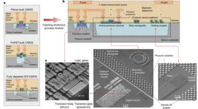
18 requires silicon photonic interconnect devices to be integrated on single chip. Although, monolithic (that is on a single chip) integration of photonic devices in close proximity to electronic circuits is crucial, recent studies has shown that it is possible to integrate photonics with silicon nanoelectronics systems on a chip [86]. The systems on chip device has successfully integrated wavelength division multiplexing (WDM) transmission link system monolithically. The study has shown that the next generation of photonic platform for computing, communications, imaging and sensing requires systems on chip.
Fig.1
.
17Photonic integration with nanoscale transistors. [Reprinted with permission A. Atabaki,et al., Nat., 556 (7701), 2018]
1.4
Purpose of Study
1.4.1
Motivation
As describe in earlier section, optical signal processing has become an attraction. Due to the high refractive index and low absorption loss of silicon, it is expected to be an outstanding candidate for replacing electrical wire. Although various silicon photonic devices have been developed, demand for a smaller footprint, lower power consumption and higher functionality remains. In addition, current optical communication is towards shorter range in which chip-to-chip also required easy monolithically integration on chip and cost effectively. This are difficult to be achieved with existing Si photonic devices.
Two-dimensional PhC structure allows strong light confinement that leads to high-Q
factor. Moreover, with the small mode volume, makes the demonstration of all-optical switching possible. Although those demonstrated devices claimed to be compatible with CMOS process, several challenges need to be overcome to integrate those devices with another Si photonic devices due to the different structure. As a result, the integration becomes more difficult.
CHAPTER 1. INTRODUCTION
19 On the other hand, PhC nanocavity requires high precision of fabrication to achieve high-Q factor. Therefore, most of the PhC nanocavity devices are fabricated by electro-beam lithography. The electro-beam lithography is an accurate fabrication process however, in term of time, the fabrication method is a time-consuming process. Hence, a stepper photolithography process, which is more commercial and widely used need to be employed. That is not all, due to the compatibility with CMOS process, this fabrication process will ease the integration of PhC device with other Si devices on the same chip.
Among various devices that has been demonstrated for optical devices, electro-optic (EO) and opto-electronic (OE) devices are the main components in order to link the electrical circuits with photonic circuits. Demonstration of EO operation is challenging because it requires low-power consumption and possible to transmit signal in fast speed. However, OE operation is more challenging because at telecom wavelength (1.55 µm), Si is transparent and photo carriers could not be generated. Therefore, complex fabrication method in which a hybrid-type photodetector such as integration of Germanium or Graphene and ion-implantation on Si has been introduced. However, it suffers for high dark current due to the presence of defect in the structure. This will lead to a disturbance of noise during data transmission.
In addition, based on Moore’s Law, there are great demand to switch from electrical circuit to optical circuit. Currently, silicon photonic based-transceiver has been commercialized by several groups. However, this device will become insufficient in the future due to the dissatisfying of optical communication demand. Since in future, the optical chip circuit are expected to be compact in size, low fabrication cost and package simplicity to extreme, researchers are start to consider for all-silicon of OE and EO scheme.
1.4.2
Objective
Recently, due to the advancement of fabrication technology process, Si PhC nanocavity has achieved high-Q factor (~105) fabricated by deep-UV photolithography fabrication process [87].
The high-Q is succeeded with the presence of SiO2 clad on the surface makes the width-modulated
line defect cavity device much stable and robust. The mode volume of the device is ~1.7 (λ/n)3.
The device was fabricated with standard CMOS process line which allowed the silicon PhC to be integrated with other devices, such as spot-size converter (SSC), heaters and p-i-n diode. This has constituted that Si PhC possible to realize integration on silicon chip and open for new possibilities for silicon photonics technology.
In this study, the application to explored high-Q photolithographically PhC nanocavity device as an optical interconnect device, namely electro-optic modulator and photoreceiver are studied. The target of the applications is towards on chip integration device with have smaller foot-print. The p-i-n diode has been embedded to the device to allow carriers injection for light modulation. Via the carrier plasma dispersion effect, the transmittance spectrum wavelength able to be modulated. Thanks to the high-Q factor, it has enabled the device to achieve large optical modulation even though the refractive index modulation is small. Thus, low power consumption is achievable. A sub-GHz modulation operation based on the carrier plasma dispersion reveals that the device has a large bandwidth modulation ability [88].
Next, the opto-electronic demonstration is demonstrated by the device. Although, it is challenging because Si is not the best candidate in term of light detection at telecom wavelength, with the high-Q factor and low leak current, it is proven that photodetection is able to be achieved.
CHAPTER 1. INTRODUCTION
20 Thus, a low-power photodetection become possible due to the all-Si device and with the help of two-photon absorption (TPA). Though similar demonstration has been done before, but with the air-clad surface, a complex fabrication process is needed specially to take care of the contact pads during the air-bridging process. Therefore, in this study, the PhC nanocavity device was cladded with silica which makes the device more stable and robust, so, the photo-detection operation demonstration becomes uncomplicated and most importantly is full CMOS compatibility [89].
Then, the combination of EO operation and OE operation as an optical transmission link is demonstrated. Since the device was made by all-Si, all-Si scheme transmission link is achievable with help of TPA effect. In addition, with the randomness structure as a detector, proved that the randomness in PhC structure possible for a practical device. The demonstration is done by detuning the resonance wavelength through temperature time dependence to match the resonance of transmitter and receiver. A sub-GHz operation was achieved. This demonstration has paved an alternative way for optical transmission as it offers small dimension and higher degree of integration with CMOS devices.
In this thesis, the contents are arranged as follows where the theory of PhC and design of the device structure will be described in Chapter 2. Next, the fabrication process of the device will be explained in Chapter 3. Then, the functionalities of the device in which as electro-optic modulator will be described in Chapter 4. The demonstration of the photoreceiver is then will be presented in Chapter 5. In Chapter 6, the demonstration of all-silicon transmission link of optical transceiver will be explained. Finally, in Chapter 7, the thesis will be summarized.
CHAPTER 2. THEORY OF PHOTONIC CRYSTAL
21
Chapter 2
Theory of Photonic Crystal
This chapter will explain the fundamental theory of PhC. The basic of PBG structure is explained which then led to the formation of cavity in the PhC. Then, the method of analysis contains of plane-wave and FDTD method which are commonly used for numerical calculation will be introduce. Later, the PhC design structure that is used in this study will be describe.
2.1
Introduction
The study of photonic crystal (PhC) had begun since 1887 by Lord Rayleigh issue of Philosopical Magazine[7]. However, no one used the term of ‘photonic crystal’. Until in 1987, American physicist who known as Eli Yablonovitch announced the name of ‘photonic crystal’ and successfully discover creation of a photonic bandgap (PBG) [4]. Then, Sajeev John has published another milestone paper on the same field by discovering photon localization in high dielectric contrast disorder superlattice microstructure which is beneficial for mechanism of non-linear application devices[8]. In this chapter, theory of PBG and cavity formation method of PhC is explained. The common method for a numerical calculation also will be described.
CHAPTER 2. THEORY OF PHOTONIC CRYSTAL
22
2.2
Photonic band structure
The existence of photonic band gap were reported in early 1990s through the solution of Maxwell’s equation [90], [91]. It has been a basis concept in understanding PhC. The utilization of PBG has been expanded by researchers. The introduction of defect in PBG structure can produce a cavity to PhC. In this section, Maxwell’s equation and the formation of cavity will be described.
2.2.1
Maxwell’s equation
The propagation of light in PhC governed by Maxwell’s equations as follows,
where E, H, D, B, ρ and J are the electric field, magnetic field, electric flux density, magnetic flux density, free charge and current density, respectively. Eq. 2.1 expresses the fact that the magnetic lines of flux form a system of closed loops. Eq. 2.2 is differential form of Faraday’s law of induction. Eq. 2.3 is differential form of Gauss’s law and Eq. 2.4 is a generalization of Ampere’s circuital law (also referred as the Biot-Savart) by the addition of 𝜕𝐃
∂𝑡, which is called the
displacement current density.
D and B can be rewrite as follows,
D (r) = ε0 ε (r) E (r) (2.5)
B
(
r
)
=
µ
0µ
(
r
)
H
(
r
)
(2.6)where ε0 and µ0 denote the electric permittivity and magnetic permeability of vacuum respectively.
However, for most dielectric material the relative magnetic permeability µ (r) is very close to unity, the Eq. 2.6 can be written as B = µ0 H.
∇ ∙ 𝐁 = 0
(2.1)∇ × 𝐄 +
𝜕𝐁
𝜕𝑡
= 0
(2.2)∇ ∙ 𝐃 = ρ
(2.3) ∇ × 𝐇 − 𝜕𝐃 𝜕𝑡 = 𝐉 (2.4)CHAPTER 2. THEORY OF PHOTONIC CRYSTAL
23
The Maxwell’s Eq. 2.1 to Eq. 2.4 become,
E and H are harmonic (oscillation) modes which can be express as,
𝐇 (𝐫, 𝑡) = 𝐇 (𝐫) 𝑒−𝑗𝜔𝑡 (2.11)
𝐄 (𝐫, 𝑡) = 𝐄 (𝐫) 𝑒−𝑗𝜔𝑡 (2.12)
Both Eq. 2.11 and Eq. 2.12 can be insert in the Eq. 2.7 and Eq. 2.9 which will describe the mode profile at the given frequency that have simple physical interpretation of there are no point sources of displacement and magnetic medium.
∇ ∙ 𝐇 (𝐫) = 0 (2.13)
∇ ∙ [𝜀(𝐫)𝐄 (𝐫)] = 0 (2.14)
The field configurations are built up of electromagnetic waves that are transverse. Therefore, if a plane wave of H (r) = a exp (jk ∙r), for some wave vector k, Eq. 2.13 and Eq. 2.14 requires that
a ∙k = 0.
For Eq. 2.8 and Eq. 2.10, the two curl equations relate E (r) to H (r)
∇ × 𝐄 (𝐫) − 𝑗𝜔𝜇0𝐇(𝐫) = 0 (2.15)
∇ × 𝐇(𝐫) + 𝑗𝜔𝜀0𝜀(𝐫)𝐄(𝐫) = 0 (2.16)
From the above equations, can be divided by ε (r) and then take the curl. The Eq. 2.15 can be used to eliminate E (r) and constants ε0 and µ0 can be combined to yield the vacuum speed of
light, c = 1
√𝜀0𝜇0. Results is express as follow,
∇ ∙ 𝐇 (𝐫, 𝑡) = 0 (2.7) ∇ × 𝐄(𝐫, 𝑡) + 𝜇0 𝜕𝐇 (𝐫, 𝑡) 𝜕𝑡 = 0 (2.8) ∇ ∙ [𝜀 (𝐫)𝐄 (𝐫, 𝑡)] = 0 (2.9) ∇ × 𝐇 (𝐫, 𝑡) − 𝜀0𝜀 (𝐫) 𝜕𝐄 (𝐫, 𝑡) 𝜕𝑡 = 0 (2.10)
CHAPTER 2. THEORY OF PHOTONIC CRYSTAL 24 ∇ × ( 1 𝜀 (𝐫)∇ × 𝐇 (𝐫)) = ( 𝜔 𝑐) 2 𝐇 (𝐫) (2.17)
From the Eq. 2.16, E (r) is obtained,
𝐄 (𝐫) = 𝑗
𝜔𝜀0𝜀 (𝐫)
𝛁 × 𝐇(𝐫) (2.18)
and for value H (r),
𝐇 (𝐫) = − 𝑗
𝜔𝜇0
∇ × 𝐄 (𝐫) (2.19)
Next, the operator Θ̂ acting on H (r) is define,
𝚯 ̂ 𝐇 (𝐫) ≜ ∇ × ( 1 𝜀(𝐫)∇ × 𝐇(𝐫)) 𝚯 ̂ 𝐇 (𝐫) = (𝜔 𝑐) 2 𝐇 (𝐫) (2.20)
In periodic structure, H (r) is assume as a periodic function. Based on Bloch-Floquet theorem, the periodic function has Bloch wavevector k which can be describe as following equation,
𝐇 (𝐫) = 𝐇𝒌(𝐫) = 𝑒𝑗𝒌∙𝐫∙ 𝐇𝑛,𝒌(𝐫) (2.21)
𝐇𝑛,𝒌(𝐫) = 𝐇𝑛,𝒌(𝐫 + 𝑎) (2.22)
a is a lattice constant value of the structure and n corresponds to the label number of primitive cells that is a part of the periodic structure. By inserting both Eq. 2.21 and Eq. 2.22 into Eq. 2.17,
Eq. 2.23 can be obtained.
(∇ + 𝑗𝒌) × 1 𝜀(𝐫)(∇ + 𝑗𝒌) × 𝐇𝑛,𝒌(𝐫) = ( 𝜔n(𝒌) 𝑐 ) 2 𝐇𝑛,𝒌(𝐫) (2.23) In Schrödinger equation, (𝜔𝑛(𝑘) 𝑐 ) 2
is eigenvalue. ωn(k) are in function ok k where it expresses the
system dispersion. H (r) in Eq. 2.22 described a Bloch function and satisfy condition below, where wavevector 𝒌′ if 𝒌′= 𝒌 +2𝜋
CHAPTER 2. THEORY OF PHOTONIC CRYSTAL
25
Since,
Following equations can be obtained.
Based on the Eq. 2.25, it is proven that Hk (r) is 2𝜋
𝒂 periodical function. Thus, the
eigenvalue ωn(k) also have same periodicity. So, in order to know the dispersion relation, it is
sufficient to know between the range of -π / a ≤ k ≤ π / a which is known as a first Brillouin zone. In most cases where time-reversal symmetry is satisfied, only half of the range is considered which is 0 ≤k≤π / a.
On the other hand, when a system is a one-dimensional structure, it has a uniform dielectric of ε (r) = 1, the dispersion diagram of the structure is shown as Fig. 2.1 (a) where the eigenvalue of Eq. 2.23 is ω(k)= ck.
However, if the system to be periodical perturbation of ∆in dielectric constant, 𝜀(𝐫) = 1 + ∆ ∙ cos (2𝜋𝐫
𝒂 ) is assumed and two eigenvalues as follows at k =π / a proportional to cos ( 𝜋𝐫
𝒂)
or sin (𝜋𝐫
𝒂) are obtained.
Eq. 2.27 and Eq. 2.28 is the origin of PBG as shows in Fig. 2.1(b). PBG works as a forbidden band for photons in the PhC structure where light within the wavelength of PBG could not enter the medium. 𝐇𝒌(𝐫) = 𝑒𝑗(𝒌 ′−2𝜋 𝑎) ∙ 𝐫 ∙ 𝐇𝑛,𝒌(𝐫) = 𝑒𝑗𝑘′𝐫 ∙ 𝐇𝑛,𝒌(𝐫)𝑒−𝑗 2𝜋 𝑎 ∙ 𝐫 (2.24) 𝐇𝑛,𝒌(𝐫)𝑒−𝑗 2𝜋 𝑎 ∙ 𝐫 = 𝐇𝑛,𝒌(𝐫 + 𝑎)𝑒−𝑗 2𝜋 𝑎∙(𝐫+a) 𝐇𝑛,𝒌′(𝐫) = 𝐇𝑛,𝒌(𝐫)𝑒−𝑗 2𝜋 𝑎 ∙ 𝐫 (2.25) 𝐇𝒌(𝐫) = 𝑒𝑗𝑘 ′𝐫 ∙ 𝐇𝑛,𝒌′(𝐫) = 𝐇𝒌′(𝐫) (2.26) 𝜔+,𝒌=𝝅 𝒂 ∝ |𝐇+| 2∝ 4cos2𝜋𝐫 𝒂 (2.27) 𝜔−,𝒌=𝝅 𝒂 ∝ |𝐇−| 2∝ 4sin2𝜋𝐫 𝒂 (2.28)
CHAPTER 2. THEORY OF PHOTONIC CRYSTAL
26
Fig. 2.1 Dispersion relation, ω vs. k for waves in one-dimensional PhC structure. (a) Dispersion diagram for a uniform dielectric material where ε (r) = 1. (b) Dispersion diagram for periodic dielectric structures where 𝜀(𝐫) = 1 + ∆ ∙ cos (2𝜋𝐫
𝒂 ).
This can be expanded into two- or three-dimensional periodic structure. But, in principle, there is no full PBG in two-dimensional PhC structure. In the case of three-dimensional periodic structure, there would be photonic bandgaps along x, y and z directions, and for difference polarizations of the dielectric field. If the refractive index contrast and the periodicity in the three-dimensional structure are such that these photonic bandgaps overlap in all directions and for all polarizations of light, a full photonic bandgap occur. As shown in Fig. 2.2 (a), the overlap frequency range ∆ω becomes full PBG in all directions and for all polarizations of light which means no light can be propagate through the structure. However, only certain three-dimensional structures allow full PBG to develop. One of the allowed structures is ‘wood pile’ periodic structure as shown in Fig. 2.2 (b). In ‘wood pile’ structure, the rods are parallel in each layer and the layers are perpendicular to each other.
CHAPTER 2. THEORY OF PHOTONIC CRYSTAL
27
Fig. 2.2 (a) Full PBG in three-dimensional PhC structure. The PBG along x, y and z are overlapping for all polarizations of field. (b) The ‘wood pile’ unit cell of PhC. The 1-4 labelled referring to the 4 layers that is parallel to each other.
2.2.2
Cavity formation
Point and line defects that occur in normal crystal, also occur in PhC structure. Fig. 2.3 illustrated the example of defects. Defects are introduced to PhC to enhance certain optical properties. Definition of defects is a discontinuity in the periodic structure. There are two kinds of defects which is point defect and line defect as shown in Figs. 2.3 (a) and (b), respectively. Point defect or so-called optical cavity, can be created by removing or altering a unit cell in the periodicity. This will lead to the trapping of light radiation within the cavity as illustrated in Fig. 2.3 (d).
Fig. 2.3 Illustration of defects in PhC structure. (a) Line defect is introduced in PhC structure. (b) An ultrasmall waveguide formed and permits light propagation only along the line defect. (c) Point defect that acts as an optical cavity to trap the light. (d) Light that has been trap (confined) inside the cavity.
CHAPTER 2. THEORY OF PHOTONIC CRYSTAL
28 Line defect
Line defects are formed when a certain row of unit cell is removed. The light is prevented from dispersing into the crystal with the presence of PBG. The guided propagating light in the PhC structure is called waveguide as shown in Fig. 2.3 (b).
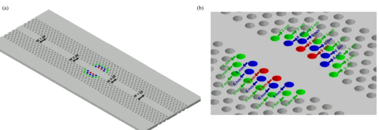
The dispersion diagram of the line defect is shown in the Fig. 2.4 and Fig. 2.5. The grey area represents the light cone where light is dissipated out of PhC slab due to the dissatisfied of total internal reflection. The orange area represents PhC modes Lattice constant, a and hole diameter is 420nm and 253nm, respectively. Line defect is introduced in the structure which W0.98 (0.98% of the original width). The inset shows the corresponding structure where the black area represents silicon material (n = 3.47) while the white area for Fig. 2.4 represents air (n =1.00) and Fig. 2.5 represents silica (n=1.44). Fig. 2.4 (a) and Fig. 2.5 (a) shows a perfect periodic PhC structure while Fig. 2.4 (b) and Fig. 2.5 (b) a line defect is introduced. It shows clearly, that two modes appear in the PBG area when line defect is introduced which represent the waveguide modes.
Fig. 2.4 Dispersion diagram of 2D PhC structure. (a) PhC structure without defect. (b) PhC structure with defect which is W0.98. The inset in (a) and (b) shows the corresponding structure. The blue line shows the even symmetry modes and the red line shows the odd symmetry modes. Insets shows the corresponding structure which represents silicon as the black area with refractive index, n of 3.47 and air as the white area with refractive index, n of 1.00.
CHAPTER 2. THEORY OF PHOTONIC CRYSTAL
29
Fig. 2.5 Similar as Fig. 2.4. Insets shows the corresponding structure which represents silicon as the black area with refractive index, n of 3.47 and silica as the white area with refractive index, n of 1.44.
Due to the difference of refractive index between air and silica, the frequency range of PBG is narrower in Fig. 2.5 since the ambience of silicon is silica which is known as silica-clad. Therefore, light is propagating in narrower frequency range in silica-clad PhC waveguides.
Point defect
In two-dimensional PhC slab waveguide, distributed Bragg reflection (DBR) of the surrounding PhC lattice influenced the in-plane defect mode confinement. With the condition that the wave vector of light at vertical is k┴and at parallel is kǁ‖to the PhC slab, wave vector of light k is
𝑘2= 𝑘∥2+ 𝑘⊥2 = (
𝑛𝑐𝑎𝑣 𝜔
𝑐 )
2
(2.29)
In total internal reflection, the light wave vector, k will satisfy the Snell’s law as follows,
|𝑘∥ 𝑘| >
𝑛𝑎𝑚𝑏
𝑛𝑐𝑎𝑣
(2.30)
The dissipation of light in defect from the slab can be calculated from the Eq. 2.29 and Eq. 2.30. The vertical confinement works as standard waveguiding by total internal reflection.If the magnitude of the in-plane momentum component, k┴, is insufficient to support guiding,
vertical radiation loss will occur. Therefore, in order to achieve high-Q factor, the vertical radiation loss have to be reduced. For an air clad PhC waveguide, due to the refractive index, n is 1, therefore k┴2 = (ω/c)2, where ω is angular frequency and c is the speed of light. Modes that
radiate vertically will have small in-plane momentum components lie within the light cone cladding.
CHAPTER 2. THEORY OF PHOTONIC CRYSTAL
30
Fig. 2.6 illustrates the light cone in two-dimensional structure. If the frequency of wavevector of light is ω0, light will not exist in the slab and dissipate to the surrounding.
Fig. 2.6 Light cone in kx, ky and ω space where k = ω ∙ (namb/c). Blue cone represents to the light
cone where in light will be dissipate from the slab in this area.
2.3
Fabry-Pérot Cavity
In order to understand the transmission spectrum of a nanocavity, Fabry-Pérot cavity is used as an example. It consists of two flat mirrors opposing each other as illustrated in Fig. 2.7 (a). When this mirror perfectly aligned to each other as parallel with free space between them, light wave reflection occurs between the two mirror M1 and M2. The light reflections wave between the
mirrors of M1 and M2 will lead to construct and destruct the interference within the cavity. During
the constructive phenomenon, it is called resonance. The series of travelled reflected waves will produce a standing light wave in the cavity as in Fig. 2.7 (b). At the resonance phenomenon,
Eq.2.31 should be satisfied;
𝑚𝜆𝑚 = 2𝑛𝐿; 𝑚 = 1, 2, 3, …. (2.31)
where m is an integer of mode number, λm is resonance wavelength, n is medium refractive index
and L is the cavity length. Fig. 2.7 (c) illustrates the intensity of the allowed modes as a function of frequency. If the mirrors are perfectly aligned, light beam will be reflecting within the mirrors and there will be no loses from the cavity, thus, sharp line peaks occur at frequencies, vm. The
frequencies at vm can be defined as Eq. 2.32.
𝑣𝑚 = (
𝑐
2𝑛𝐿) 𝑚 (2.32)
However, in some cases there is possibility that some light radiation will escape from the cavity caused by the imperfectly mirror reflecting, hence, the mode peaks will appear less sharp and finite.
Refer to Fig. 2.7 (a), light wave will be travelled as wave Y after wave X completing a round trip. In the imperfection of reflections cases, wave Y has different phase and magnitude compared to wave X. If the value of reflection coefficient of mirror M1 and M2 are same as