! "
#
$ $
&
&
!
" #
&
()
!" !#$%&
'($)$!
)$*
'+$* $#$ +,# %$!
'+$* &!($)-.
*
'
$
+' %
,' %
*
- ' '- '
'
.
'
/' %
# '
-
' '-
' '
-'
0'
- ' -
'
1'
*
-'
2' 3
4
-
-
%
5
6
(
'
7' #
-
-
-8' ,
-
'
9' ,
(
4,
! 6- :.
&
<'
,
, -
.
5
'
+='
(
4 & - %
- )
- ,
6-'
++' ,
(
:
>
; 4, -
- ?
- . 6
?
' :#
!
"
'
+/'
(
@=/
@=0
'
+0' ,
- % *
- %
- , A- >
-
'
+1'
(
(
!
,-'
+2'
- B
-
(
C. .
-'
()
- ,
'
5
- /1
/==8
A
>,3, ,) C
3 '''''''''''''''''''''''''''''''''''''''''''''''''''''''''''''''''''''''''''''''
>,3, ,) C
3 4#)
!# 6 '''''''''''''''''''''''''''''''''''''''''''''''''''''''''''''
>,3, ,)
!
C ,)''''''''''''''''''''''''''''''''''''''''''''''''''''''''''''''''''
>,3, ,)
)
,>,)'''''''''''''''''''''''''''''''''''''''''''''''''''''''''''''''''''
&
>,3, ,)
!
%,>,)''''''''''''''''''''''''''''''''''''''''''''''''''''''''''''''''
&
!)5, ,,) . , 3#,) .,!5, ''''''''''''''''''''''''''''''''''''''''''''''''''''
&
., ,
) ,) ,! '''''''''''''''''''''''''''''''''''''''''''''''''''''''''''''''''''''''''''''
&
,
,! # # ''''''''''''''''''''''''''''''''''''''''''''''''''''''''''''''''''''''''''''''''''''''''''''
A
,
,!
, %,! '''''''''''''''''''''''''''''''''''''''''''''''''''''''''''''''''''''''''''''''
A
,
,! ,% 3 ''''''''''''''''''''''''''''''''''''''''''''''''''''''''''''''''''''''''''''''''''''
A
,
,! 3,
#!,) ''''''''''''''''''''''''''''''''''''''''''''''''''''''''''''''''''''''''''''
A &
#) # ,!# ''''''''''''''''''''''''''''''''''''''''''''''''''''''''''''''''''''''''''''''''''''''''''''''''
A&
,%
!,D '''''''''''''''''''''''''''''''''''''''''''''''''''''''''''''''''''''''''''''''''''''''''''''
A&
%,% #'
) ,> 3 ,) '''''''''''''''''''''''''''''''''''''''''''''''''''''''''''''''''''''''
+
A
#'9
''''''''''''''''''''''''''''''''''''''''''''''''''''''''''''''''
1
%,% ##'
, ,!
!# ''''''''''''''''''''''''''''''''''''''''''''''''''''''''''''''''''''''''''
7
/'+
, 9< 2+'''''''''''''''''''''''''''''''''''''''''''''''''''''''''''
7
/'+'+
'''''''''''''''''''''''''''''''''''''''''''''''''''''''''''
9
/'+'/ !
'''''''''''''''''''''''''''''''''''''''''''''''''''''''''''''''''''''''''''
9
/'+'0
#
'''''''''''''''''''''''''''''''''''''''''''''''''''''''''''''
++
/'+'1
#E
'''''''''''''''''''''''''''''''''''''''''''''''''''''''''''''''''
+1
/'+'2
#
$
''''''''''''''''''''''''''''''''''''''''''''''''''''''
+0
/'/
D '''''''''''''''''''''''''''''''''''''''''''''''''''''''''''''''''''''''''''''''''
+7
/'0
D '''''''''''''''''''''''''''''''''''''''''''''''''''''''''''''''''''''''
+8
/'1
FFFFFFFFFFFFFFFFFFFF'''
+9
/'2 ,
4#
$ 6 DFFFFFFFFFFFFFFFF +<
%,% ###'
!,)D,) ,) '''''''''''''''''''''''''''''''''''''''''''''''''''''''''''''''''''''
/+
0'+
.
,
!
!
'''''''''''''''''''''''''''''''''''''''''''''''''''''''''''''''''''''''''''''
/+
0'/ ,
! /0/''''''''''''''''''''''''''''''''''''''''''''''''''''''''''''''''''''''
/0
0'0
$
D '''''''''''''''''''''''''''''
/1
0'1
$
'''''''''''''''''''''''''''''''''''''''''''''''''''''''''
/2
0'2
$
''''''''''''''''''''''''''''''''''''''''''''''''''''''
/7
0'2'+ !
''''''''''''''''''''''''''''''''''''''''''''''''''''''''''''
/7
0'2'/ !
!
''''''''''''''''''''''''''''''''''''''''''''''''''''''''''''''''
/8
0'/
$
3
''''''''''''''''''''''''''''''''''''''''''''''''''''
/9
A
0'7'/
D''''''''''''''''''''''''''''''''''''''''''
/<
%,% #B' >, #3
,)
%,>, ,) '''''''''''''''''''''''''''''''''''''''''''''''''
01
1'+
$
''''''''''''''''''''''''''''''
01
A
/
/'+ %
,
3 , 9< 2+''''''''''''''''''''''''''''''''''''''''''
7
/'/ ,
% !
?''''''''''''''''''''''''''''''''''''''''''''''''''''''
9
/'0 !
#
,
3 , 9< 2+''''''''''''''''''''''''
++
/'1 3
D
%%%%%%%%%%%%%%%%%%%%%%%%%%%%%%%%%%%%%%
+8
/'2
%
#D 3/<0 ''''''''''''''''''''''''''''''''''''''''''
+8
/'7 %
''''''''''''''''''''''''''''''''''''''''''''''''''
+<
/'8 #
,G /0/ ''''''''''''''''''''''''''''''''''''''''''''''''''''''''
/=
0'+
.
,
!
!
''''''''''''''''''''''''''''''''''''''''''''''''''''''''''''''''''''''''
/+
0'/
!
.
D '''''''''''''''
//
0'0 .
,G/0/-
-
D'''''''''''''''''''''''''''
/0
0'1 .
- 3/<0 -
D '''''''''''''''''''
/2
0'2'!
''''''''''''''''''''''''''''''''''''''''''''''''''''''''''
/2
0'7 !
''''''''''''''''''''''''''''''''''''''''''''''''''''''''''''''''
/7
0'8 !
!
''''''''''''''''''''''''''''''''''''''''''''''''''''''''''''''''''''
/8
0'9
,
3
''
/9
0'<
D
!
A
/
/'+
)
()
% .
!
D )'''''''''''''''''''''''''
<
/'+
)
()
% .
!
D ) ''''''''''''''''''''''''
+=
/'/ !
# ''''''''''''''''''''''''''''''''''''''''''''''''''''''''''''''''''''''''''''''''
+/
/'0
#
''''''''''''''''''''''''''''''''''''''''''''''''''''''''''''''''''''''
+0
/'1
''''''''''''''''''''''''''''''''''''''''''''''''''''''
+2
/'2 3
,
3/<0 '''''''''''''''''''''''''''''''''''''''''''''''''''''''''''''
+9
0'+ ,
,
)
>
'''''''''''''''''''''''''''
0/
0'/ ,
- )
%
-
)
>
''''''''
0/
1'+
'''''''''''''''''''''''''''''''''''''''
02
1'/
D ''''''''''''''''''''''''''''''''
07
A &
,'
''''''''''''''''''''''''''''''''''''''''''''''''''''''''' 3+
%' !
3
!
'''''''''''''''''''''''''''''''' 3/
A&
-$
'
(
'
'
'
, 9< 2+
D
'
&
'
E
-, 9< 2+
'
-$
$
'
$
3/<0 '
>
-
*
'
0 . '
-A&
/
#
-
*
$
&
$
*
&
'
$
*
' #
-$
*
'
$
$
'
*
$
$
&
- *
$
$
* *
' ,
$
*
'
A
$
$
$
$
9
1 $
1
$
$
'
(
$
$
E
$
-$
4 D6'
$
D
&
# 4
$
#
$ 6'
$
$
-
$ $
-
$
$
4 D6
$
* $
' ,
D
*
&
-
$
$
*
&
D
H
&
$
D
*
$
*
'
,
-
4
6 $
9
$
' ,
A
*
$
0 . '
-!"#
$ %&
' $() "#
$() "#
+
'
*
,
'
*
$ %&
$() "#
-,
-!
!
.
#
'
*
'
/
+
/
' $() "#*
!
#
(
'
*
+
/
0
"
-
01
01
/1
! "
# #
$
.
#
$() "#
0
$
%
# #
,
.
#
$
,
+
$
&
' ' ' #
# #
-!
.
#
!
+
,
/
,
!
2
0
!
( )#
#
#
"
2
,
! ' #
2
!
$() "#
*
2
!
+
#
,
2
+
- # .
)
!
"
#$
%
&
(
)
*
+
!
&
&
&
,- . *
&
&
/ *
& ' &
&
+
&
/
# 01
&
#2
& &
3
& &
&
&
# 01
# 01
&
& &
&
&
# 01
'
&
'
4
*
&
&
'
/
&
/
&
0
&
0'
&
&
50
6 776
0
6
(76
6 776
& +
&
8
&
& & 9
:
;
&
9
;
!& &
&
0 0(*
+
&
- )
&
&
<
0
&
==9
;
0
&
#
*
9
; " &
&
%
0
&
"
0
&
7
*
" &
&
"
& &
*
&
&
&
&
>
0
&
5 9
;
0
&
'
*
" &
&
5
-
9
;
0
&
&
9
; &
&
(
&
& &
!"
!#
*
& /
?
& & & /
& & +
0
$
9'
0;
0
&
&
,
&
' $ 9
<
% ;
' 6 9
<
> ;
'
0
+
%
,
& &
&
&
&
1@A
*B'
0
,
0
&
3
&
&
,
&
C/
* *
%
&
&
6
'6
$
"6*
&
'
&
$
=6
6
-6
(
0
&
=12 9
(
;
0
&
( *
/
&
<
2
" .
0
&
=12
& &
2
1'
=12 (
$
2
" .
0
&
=12 9
+
;
& &
2
D7%
=12 %
*
'
=12
(
$ (
'$
=12
+
0
&
&
&
4
&
& *
& & /
&
& &
&
0
&
&
+
9 #;
6
&
%
9 ;
" 6
0
&
=12 9
&
;
0
&
8
&
8
&
)
'
*
&
4
,
* &
+
&
,
0
&
1' 9
&
-0
&
8
&
0
&
=12 9
;
0
&
8
&
!
" "
"#
&
& *
< %
&
* %
&
?
&
&
!&
&
& /
4
/
&
#
70
#
+
&
4 &
&
& /
D
% >
+
#
#$
!
0
&
#
#$
7
& 8
&
#
% >
#(
&
&
&
"
&
&
9
;* &
&
&
9
$
;
#,
#
&
/
#-
&
4 &
&
* &
&
#-
&
#>
#
*
%
#%
#
&
&
&
&
* &
/
&
,
0
&
#
$
%"
#
# (
)
&
& & /
&
# ,
=
#
=
#
# -
"
4 &
&
#
# >
"
4 &
&
.
(
#A
# %
"
4 &
&
,
#
#
"
4 &
&
.
(
#A
#
"
4 &
&
,
&
&
&
&
* &
&
&
&
&
"
&
/
&
&
&
&
&
&
2
+
/
&
&
&
= )
/
& /
&
&
&
>
!
&
&
$
%"
(
=
,
=
=
-
"
&
&
>
"
&
&
A
%
"
&
&
,
"
&
&
A
"
&
&
,
& $
'
C1
&
&
,
9
&
&
& /
&
;*
. /
9
&
/
&
/
!&
")7
&
+
-
3
*
&
?
0A'*
&
A'
8
&
0
'
&
C
. /
-%
C
%
*
&
9
;*
9
;*
&
9
;
&
* &
&
0"
&
=12
1
4
>
%
C
>
&
9
;*
*
*
&
9
;
&
"
"
&
=12
&
*
&
0"
&
=12
1
C>%
C,- 8
&
&
-
>
C
>
&
9
;*
9
;*
*
&
9
;
& & &
%
/
4
$
"
1
/
&
&
&
!"
&
*
&
/
& &
C
&
*
&
&
C % 8
&
&
"
1'
&
=12
%
1'E
C>% 8
&
&
*
+
1'E
C,- 8
&
&
1
>
/
.
(
1
>
&
<
>%
F
G
G
.
(
1
=
9> ;
.
8
&
+
8
&
&
<
;
+
&
H
I
H/
I*
* %*
>
%;
)
+ 9
$
;
&
1
(
"(
)
'
* +
, )
,
>%
;
% ,
9
%
×
−
×
%
×
9
% ,
−
;
×
,
'-& * +
'! * +
!
>%
;
% ,
9
,
.
'=
&
&
&
&
+
C
&
+
&
'=
'=
!
'=
&
& &
*
<
0
.
C
& &
&
J
& &
*
&
8 K
%
*
&
&
&
'=
/
&*
&
& 4
& &
.
&
&
*
&
&
&
&
&
&
&
+
&
'=
'=
0
' &
/
&
'=
(
&
/
/
'=
0
&
'=
9
0
;
0
<>
J
>
'=
&
0
'=
D6> D
&
$
'=
!
.
)
&
'=
&
.
*
= $% >'
.
'= 9
0
;
&
$% >'
&
&
&
,
-
@
>, @
,!.
* &
*
/*
&
&
$
= $% >'
4 %
'= =
-9
*
%*
>*
-;* -
9
*
%*
>*
-;*
%
9
*
%;
&
+ & &
<
$
& $% >'
#
%
1
1 %
'=
6
6
6
$
$
'
6
6
$
6
$
6
$
6
$
6
6
$
$
$
$
'
$
6
6
$
$
'
&
$
&
& &
&
&
&
&
C
& & &
&
"
&
&
&
& &
&
(
0 2
(
0
&
&
9
0
;
&
&
&
&
*
+
+
&
&
&
+
.
+
*
+
+
& &
&
& &
+
&
1
&
*
* &
&
8
(
0
*
&
"
(
0
% ,
-
"
(
0
"
/
0
*
9
;
9=1 ; .
&
&
&
&
*
?
*
&
& &
&
&
/
&8
!. /
&
&
&
'"
6
&
&
&
4
$
= 1
)
&
/*3*
.
.
4
0 %>%
@
@ &
&
/*3*
.
.
A %>% =
-
.
*
%
.
4
$C= 1
4
0 %>%
.
4
0 %>%
%
Diagram kotak dari Pengendali Putaran Arah Rumah pada Pemodelan
Rumah Pintar dapat ditunjukkan pada gambar dibawah ini:
!
Diagram Kotak Pengendali Putaran Arah Rumah Pada Pemodelan Rumah PintarPC dalam hal ini berlaku sebagai
yang berfungsi untuk
memberikan input dari
(
),
memberikan
perintah untuk kemudian diteruskan kepada mikrokontroler untuk kemudian
proses pengendalian dilakukan. Sebaliknya,
juga akan menerima tampilan
berhasil atau gagalnya suatu perintah dari PC.
Seperti dijelaskan pada dasar teori bahwa antarmuka berfungsi sebagai
22
mengubah level logika antara kedua blok tersebut (PC dan mikrokontroler) dalam
komunikasi serial.
!
"
Gambar Pemodelan Rumah dan Koneksinya ke PC
Sensor posisi disini akan memberikan referensi kepada mikrokontroler
tentang arah rumah pada saat ini. Sehingga mikrokontroler dapat menentukan
kearah mana dan pada posisi mana motor harus berputar untuk mendapatkan
posisi yang diinginkan. Setelah berputar, sensor ini juga akan memberikan
informasi kepada mikrokontroler apakah posisi yang diinginkan tercapai. Gambar
pemodelan rumah pintar dan koneksinya dapat dilihat pada gambar 3.2.
Setelah mendapatkan perintah, mikrokontroler akan mengendalikan ke
arah mana semestinya motor DC berputar melalui driver motor DC, dalam hal ini
driver yang digunakan adalah L293D. Motor DC secara tidak langsung akan
memberikan umpan balik kepada sensor. Motor DC akan berputar dan
menyebabkan sensor posisi
mendeteksi perputaran dari motor DC yang
kemudian akan memberi referensi kepada mikrokontroler.
Posisi rumah pada awal pengendalian sudah terlebih dahulu diatur
23
dengan menggunakan kompas analog. Kompas ini juga digunakan untuk
mendapatkan arah mata angin yang presisi untuk arah rumah yang lain. Untuk
program, pengaturan posisi
dilakukan oleh PC.
"
#" "
Untuk berhubungan dengan
pada
, tegangan pada
mikrokontroler harus diubah dahulu dari standar TTL ke standar RS232.
Sebaliknya,
pada P
juga harus mengubah level tegangannya dari
standar 232 ke standar TTL.
Untuk itu digunakan IC MAX232 yang memiliki 2 buah pengubah
tegangan dari standar TTL ke standar RS232 dan 2 buah pengubah tegangan dari
standar RS232 ke standar TTL. Pada IC MAX232 ini perlu ditambahkan
beberapa kapasitor untuk menunjang fungsinya sebagai pengubah level tegangan.
Koneksi dan besarnya kapasitor disesuaikan sesuai dengan
.
Koneksi antara MAX232, mikrokontroler, dan PC ditunjukkan pada
gambar 3.3.
!"
!"
!" !"
!"
# $
24
$
Arus yang dihasilkan oleh mikrokontroler melalui keluaran dari pin,pin
port 0 sebesar maksimal 15 mA, belum mencukupi untuk menggerakkan motor
DC yang membutuhkan arus rata,rata sebesar 185mA. Untuk itu diperlukan suatu
komponen penggerak motor DC yang mampu memenuhi kebutuhan besar arus
yang semestinya dapat menggerakkan motor DC tersebut. Untuk itu digunakan
suatu
motor DC
motor DC yang digunakan disini adalah IC L293D. IC ini
mampu menggerakkan suatu motor DC dengan arus keluaran mencapai level
maksimum 1,2 A. dan hanya dengan masukan arus input minimum 0,1 mA untuk
masukan nilai tinggi (
). Arus ini masih dibawah nilai arus keluaran dari
mikrokontroler. Semua nilai,nilai tersebut terdapat pada
masing,
masing komponen.
Motor DC akan berputar searah jarum jam apabila sebelumnya masukan
1 (
) pada
mendapat logika tinggi (H) dan masukan 2 (
) mendapat
masukan berupa logika rendah (L) dari mikrokontroler. Sedangkan untuk putaran
berlawanan jarum jam, terjadi hal yang sebaliknya.
mendapat masukan
rendah dan
mendapat masukan tinggi. Dari kedua kondisi tersebut,
pada driver harus terlebih mendapat masukan tinggi dari mikrokontroler.
Koneksi antara mikrokontroler,
motor DC, dan motor DC
25
%
& & &
#& #&
! ! ! ! &
'
'
'
!
%
Koneksi Mikrokontroler, L293D, dan Motor DC
%
$
&
&
& &
Sensor posisi di sini yang digunakan adalah
. Dengan posisi
awal (default) dari model rumah pintar tersebut menghadap utara. Sensor
mempunyai arus maksimal sampai 1 A. Namun pada perancangan ini
menggunakan arus sebesar 10mA agar arus yang mengalir tidak melebihi batas
arus maksimal dan mampu mampu mengalir pada mikrokontroler.
!
'
Rangkaian
Cara kerja dari rangkaian pengaman jendela adalah
yang
bersifat seperti saklar saat didekatkan pada medan magnet maka
dalam kondisi ON sedangkan saat jauh dari efek medan magnet, maka
dalam kondisi OFF. Dari kondisi ini maka pada pemasangannya
diletakan sesuai dengan arah,arah rumah yang diinginkan (8 arah mata
angin), jadi
yang digunakan berjumlah 8 buah. Sedangkan magnet
26
magnet yang berputar mendekati salah satu dari dari
maka arus akan
mengalir melalui
tersebut yang kemudian akan memberikan referensi
kepada mikrokontroler tentang posisi sensor
yang ON.
'
$
(
Selain Perancangan koneksi,koneksi mikrokontroler dengan perangkat
yang lain. Juga dijelaskan perancangan mikrokontroler tersebut sendiri.
Mikrokontroler juga membutuhkan adanya osilator dan adanya rangkaian reset
yang digunakan untuk menset kembali mikrokontroler ke keadaan semula.
'
)&
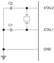
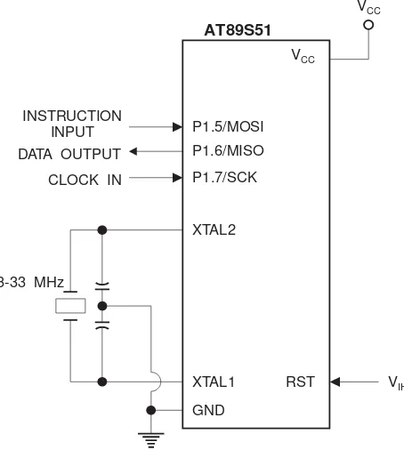
Mikrokontroler mempunyai rangkaian osilator internal (
) yang merupakan sumber
!
bagi CPU. Untuk dapat
menggunakan rangkaian osilator dalam chip, ditambahkan 1 buah
kristal dan 2 buah kapasitor pada pin XTAL dan pin XTAL2 (pin 18
dan 19)
[1]. Rangkaian ini menggunakan kristal 12 MHz dan 2 buah
kapasitor 30 pF sehingga frekuensi detak pada CPU adalah 12 MHz.
() *"
*" +
+ %
% +#
%#, # ,
, , , , , , , , ,
, , , , ,
,-, ,
, , , , , , ,
27
' "
&
Rangkaian ini digunakan untuk mereset mikrokontroler
pada saat catu daya dihidupkan. Keadaan reset pada mikrokontroler
diperoleh apabila pin reset diberi logika tinggi
[1]. Waktu reset tersebut
dihitung dengan rumus T=RC. Waktu reset 100ms dengan C=10uF
maka resistansi:
=
=
=
− − − − 3 6 3 6 310
*
10
)
10
*
10
/(
)
10
*
100
(
*
)
10
*
10
(
10
*
100
Cara kerja reset ini adalah bila saklar reset ditekan maka
aliran arus mengalir dari Vcc melalui resistor 1kD menuju kaki reset:
54
,
4
)
10
*
10
(
)
10
*
1
(
5
*
)
10
*
10
(
3 3 3 9=
+
=
"
. + + % % +# %#, # , , , , , , , , , , , , , , , ,-, , , , , , , , , !" / /28
*
$
Mikrokontroler dapat bekerja bila dimasukkan instruksi,instruksi yang
diprogramkan. Program dalam perancangan ini terdiri dari bagian program utama
dan program sub rutin penggerak motor DC. Program utama adalah program
rutin yang mencakup seluruh kerja dari program. Mulai dari komunikasi dengan
PC sampai dengan bergeraknya motor DC. Sedangkan
sub rutin penggerak
motor DC mencakup pengolahan data dari PC sampai pada keputusan,keputusan
dari mikrokontroler yang harus diambil tentang berputarnya motor DC.
*
,
(
.
29
Rutin utama perangkat lunak pada mikrokontroler akan
menginisialisasi
fasilitas,fasilitas
yang
akan
digunakan
pada
mikrokontroler. Mikrokontroler akan memulai rutin untuk transfer data
secara serial dari komputer ke mikrokontroler. Setelah transfer selesai,
data tersebut akan diolah oleh mikrokontroler yang selanjutnya
digunakan untuk menggerakkan motor DC.
Diagram
alir
rutin
utama
perangkat
lunak
pada
mikrokontroler ditunjukkan pada gambar 3.8
* " # !
(
Sub rutin penggerak ini diawali dengan inisialisasi
komunikasi serial antara PC dan mikrokontroler. Pada komunikasi serial
ini terlebih dahulu harus diatur dua hal terlebih dahulu. Yaitu
menentukan mode serial yang akan digunakan dan menentukan
. Penentuan mode serial dilakukan dengan mengisi register SCON.
Pada perancangan ini mode serial yang digunakan adalah mode 1. yaitu
menggunakan 8 UART dengan
yang dapat diatur.
Pada mode ini, komunikasi data dilakukan secara 8 bit data
asinkron, yang terdiri dari 10 bit. Yaitu 1 bit start, 8 bit data, dan 1 bit
stop.
#
pada mode ini dapat diatur dengan menggunakan
1. Port 3.0 pada mikrokontroler berfungsi sebagai RxD, yaitu port untuk
menerima data serial, dan port 3.1 berfungsi sebagai TxD, yaitu port
30
Untuk pengaturan
port serial, yakni dengan
mengubah bit SMOD yang terletak pada register PCON menjadi logika
tinggi. Penghitungan
dapat dihitung sebagai berikut:
32
*
_
1
_
1
_
#
=
Jika diinginkan
2400bps,
1 harus diatur
agar
setiap
32
*
2400
1
detik. Timer
setiap kali TH1
mencapai nilai limpahan dengan frekuensi sebesar f
osc/1,0592 atau
periode sebesar 11,0592/f
osc. Dari sini akan diperoleh rumus sebagai
berikut:
32
*
2400
1
)
1
256
(
*
0592
.
11
=
−
$%
244
240
*
32
*
0592
.
11
256
1
=
−
≅
$%
Dengan frekuensi osilator sebesar 11,0592*10
3Hz, maka TH1 adalah
244 atau 0F4H.
Selanjutnya data yang telah tersimpan di akumulator akan
diambil untuk selanjutnya diolah. Kemudian data yang telah diambil
tersebut akan dibandingkan. Disini data dari PC yang telah tersimpan di
akumulator adalah data berupa nilai heksadesimal yang mewakili arah
mata angin. Sebagai contoh arah utara terwakili oleh nilai 46H. Dan
31
!
Arah Mata Angin dan Nilai Heksadesimalnya
01 0 0 &23&
3403 5(6/'076'38049
0 0 (
38! %0! (
38! (
6&220 0 ( +640 0& (
$0 0 0:0 $(
$0 0 (
$0 0 %0! (
Selanjutnya jika sudah terdefinisi data yang masuk, akan
dicek dimanakah letak/posisi dari motor DC atau arah rumah tersebut
menghadap. Pengecekan dilakukan dengan melihat isi dari port 0. Port 0
merupakan port yang digunakan sebagai port masukan dari sensor
posisi.
yang memberi masukan on, akan memberikan
masukan berupa logika tinggi (1) kepada mikrokontroler. Sedangkan
yang off akan memberi masukan berupa logika rendah (0).
Sehingga dari kedelapan arah mata angin yang ada akan memberikan
input masing,masing yang membentuk data 8 bit pada port 0. Arah mata
angin, nilai binernya, dan nilai heksadesimalnya dapat dilihat pada tabel
3.2.
!
"
Arah mata angin, Nilai Biner, dan Nilai Heksadesimalnya
01 0 0 &23& $3&6 5 ;3 9 (6/'076'3804
0 0 (
38! %0! (
38! (
6&220 0 (
+640 0& (
$0 0 0:0 (
$0 0 (
32
Setelah didapat posisi rumah pada saat itu, kemudian
motor DC akan digerakkan ke posisi yang diinginkan. Sebelum itu,
diberikan terlebih dahulu perintah untuk mengaktifkan driver motor DC
lewat
&
nya. Perintah tersebut dilakukan dengan memberi logika
tinggi (
) pada port P1.2 yang merupakan output mikrokontroler ke
motor DC pada pin
. Arah putaran dari motor DC
disesuaikan dengan posisi rumah sebelumnya. Apabila arah putaran
yang diinginkan sesuai dengan arah jarum jam, maka port P1.0 yang
harus di,
. Sedangkan arah putaran yang berlawanan dengan jarum
jam, maka port P1.1 yang harus di,
.
Jika arah putaran motor DC telah terlaksana, maka langkah
selanjutnya adalah mengatur agar motor berhenti pada posisi yang
diinginkan. Caranya adalah dengan mengecek port masukan dari sensor
(port 0), apakah port telah menunjukkan nilai yang diinginkan. Jika
belum, maka motor akan tetap berputar sampai posisi yang diinginkan
tercapai.
Diagram alir rutin penggerak motor DC ditunjukkan oleh
gambar 3.11. Pada diagram alir tersebut, hanya mewakili proses
pengecekan dan pemutaran motor DC ke arah utara saja. Untuk ke arah
lain, terwakili oleh percabangan ke arah titik,titik (percabangan untuk
data 47H, 48H, 49H, dan seterusnya sampai yang terakhir 4DH) dan
33
!
.
Diagram alir Penggerak Motor DC dari penyimpanan di Register
!"
#
$%& ' (
)
* $
(
+ "
*
'!
! " !" #
" ! !
$ !!#
# !
,
-))./!0
*
$
(
*
* 0
*
*
-))
-))
! 0
"
+ "
1
'2
!
)
+ &
%& %%& %& %%&
! ' ( #
( "
( $ # "
) "* + + # "
+ + " # !$#
3
3
$
(
" *
" $
(
"
+ &!4 0
" "
* $
(
&
* &+'
0
1
3
3
$
(
3
* &&! 0
" *
)
"
*
+ +!+ 0
" "
&
)
"
3
" &
+ 2&4 0
5
+ !&' 0
'4
0
0
6
+ &
+ &
1
5
5
)
"
#
!
$
%
7
)
$
(
$
(
!"
1
88
+ '
"
9
, * -.
. . .
. '
. / 0
'
%
)
3
:
,
3
)
*
*
1
* 3
$ "
&(
1
3
+!
*7
1
%
$
(
1
6
'
3
!
*"*
*$
5
5( 6
3
7
&& !
*:
&& !
*, $
(
,
$
(
)
7
3
)
1
;
3
)
' #
-6
)
,
7
3
)
0
1
)
" *
*1
'
)
$
(
!
"
#
$
%
&
"
&
'
(
!
"
#
$% &
'
%
()
*
"
#
%
+
,-.. /
%/
-
0)( 1
1
,-.. %%
*
/
-
2 '
!
,-.. %%
*
/
-
3 ('4
5
,-.. %%
*
/
! "#$ % &&
' $(
)
* $ % + , - . /
0 $ % 1
2 34 ) % 3
' 2 34 %
) 2 5 34 ) % 6+70
* * % 8 9
: 2 34 % 9
# 2 34 % 9
2 34 % 9
% ; ; % 9
5 9 %
8 % ;'3 5 9 %
* 5 ; 9
' : 5 ; 9
) $ 5 ; 9 % &&
* <
< =: 7 3 9>
5
8 5 9 %
2 3 % 93 99 9
9 ) 5 ? ?
+) +)
+) 58 34 3 9 >
) +:
* +: 5
+( 2 3
+# 58 34 3 9 9
>
: % ; 9 9 2
:
: % ; 55@
: 2 3
' :+ 8 5 9
) :$ 9
* :$ 58 34 3 9 9 >
( % ; 9 9 2
(
( % ; 55@
( 2 3
( 58 34 3 5 >
(* 8 5 9
(( 9
' (( 58 34 ) 3 9 9 >
) (< % ; 9 9 2
* $
$ % ; 55@
$ 2 3
$ 58 34 3 5 >
$) 8 5 9
$: 9
$: 58 34 3 9 9 >
$# % ; 9 9 2
' #
) # % ; 55@
* # 2 3
# 58 34 3 5 >
#' 8 5 9
#+ 9
#+ 58 34 3 9 9 %
, >
#$ % ; 9 9 2
#<
#< % ; 5@
' < 2 3
) < 58 34 3 5 >
* < 8 5 9
<* 9
<* 58 34 3 9 8 9 % >
<( % ; 9 9 2
<#
<# % ; 5@
2 3
58 34 3 5 >
' 8 5 9
) ) 9 8
* ) 58 34) 3 ) 9 %
' : % ; 9 9 2
' $ '
' $ % ; 5@
' < 2 3
' 58 34 3 ' 5 >
' )
' 8 5 9
') '
'* ' 58 34 ' 3 ; ; ;
) + 5
) $ 58 34 3 9
) % ;
)
) % ;
) 2 3
)' 58 34 3
)) * 8
)* ( 9
* ( 58 34 3 9
* < % ;
*
* % ;
* 2 3
* 58 34 3
* ) 8
*' : 9
*) : 58 34 ) 3 9
** # % ;
% ;
2 3
58 34 3
' 8
+ 9
+ 58 34 3 9
' $ % ;
) <
* < % ;
2 3
58 34 3
8
* 9
* 58 34 3 9
( % ;
#
' # % ;
) 2 3
* 58 34 3
8
) 9
) 58 34 3 9 8
: % ;
$
$ % ;
< 2 3
' ' 58 34 3
) ' 8
* '' 9 8
'' 58 34) 3 )
'+ % ;
'( '
'( % ;
'# 2 3
) 58 34 3 '
' ) 8
* )
) 58 34 ) 3
)* 5
)+ 2 3
)( 58 34 3 9
)< % ;
*
* % ;
' * 2 3
) * 58 34 3
* *) 8
*: 9
*: 58 34 3 9
*# % ;
+
+ % ;
+ 2 3
+ 58 34 3
' +' 8
) ++ 9
* ++ 58 34 ) 3 9
+$ % ;
+<
+< % ;
: 2 3
: 58 34 3
: 8
:* 9
' :* 58 34 3 9
) :( % ;
* :#
' :# % ;
' ( 2 3
' ( 58 34 3
' ( 8
' () 9
' () 58 34 3 9
' (: % ;
'' ($
') ($ % ;
'* (< 2 3
) $ 58 34 3
) $ 8
) $' 9
) $' 58 34 3 9 8
) $+ % ;
) $(
) $( % ;
)' $# 2 3
)) # 58 34 3
)* # 8
* # 9 8
* # 58 34) 3 )
* #: '
* #: % ;
* #$ 2 3
* #< 58 34 3 '
*' < )
*) < 8
<
< 58 34 * 3
<) 5
<* 2 3
<: 58 34 3 9
<# % ;
' % ;
) 2 3
* 58 34 ) 3
' 8
+ 9
+ 58 34 3 9
$ % ;
<
< % ;
2 3
' 58 34 ) 3
) 8
* * 9
* 58 34 3 9
( % ;
#
# % ;
2 3
58 34 ) 3
8
' ) 9
) ) 58 34 3 9
* : % ;
$
$ % ;
< 2 3
58 34 ) 3
8
' 9
' 58 34 3 9
' + % ;
) (
* ( % ;
# 2 3
58 34 ) 3
8 9
58 34 3 9 8
* % ;
:
' : % ;
* < 58 34 ) 3 8
9 8
58 34) 3 )
) % ;
+ '
+ % ;
( 2 3
' # 58 34 ) 3 '
) )
* 8
58 34 + 3% ,
' 5
) 2 3
+ 58 34 3 9
$ % ;
' <
) < % ;
* ' 2 3
' ' 58 34 3
' ' 8
' '* 9
' '* 58 34 3 9
' '( % ;
' '#
' '# % ;
'' ) 2 3
') ) 58 34 3
'* ) 8
) )) 9
) )) 58 34 3 9
) ): % ;
) )$
) )$ % ;
) )< 2 3
) * 58 34 3
)' * 8
)) *' 9
)* *' 58 34 ) 3 9
* *+ % ;
* *(
* *( % ;
* *# 2 3
* + 58 34 3
* + 8
* + 9
*' + 58 34 3 9
*) +* % ;
** +:
+: % ;
+$ 2 3
+< 58 34 3
: 8
: 58 34 3 9 8
:) % ;
' :+
) :+ % ;
* :( 2 3
:# 58 34 3
( 8
( 9 8
( 58 34) 3 )
(' % ;
(* '
(* % ;
' (: 2 3
) ($ 58 34 3 '
* $ )
$ 8
$ % ,
$ 58 34 : 3%
$ 5
$' 2 3
$* 58 34 3 9
' $( % ;
) $# % ,
* $# % ;
# 2 3
# 58 34 3% ,
# 8
#) 9
#) 58 34 3 9
#: % ;
#$ % ,
' #$ % ;
) #< 2 3
* < 58 34 3% ,
< 8
<' 9
<' 58 34 3 9
<+ % ;
<( % ,
<( % ;
<# 2 3
' 58 34 3% ,
) 8
* 9
58 34 ) 3 9
* % ;
: % ,
: % ;
$ 2 3
< 58 34 3% ,
8
' 9
) 58 34 3 9
* ) % ;
+ % ;
( 2 3
# 58 34 3% ,
8 9
58 34 3 9 8
' ' % ;
) * % ,
* * % ;
' : 2 3
' $ 58 34 3% ,
' 8
' 9 8
' 58 34) 3% , )
' % ;
' ) % , '
'' ) % ;
') + 2 3
'* ( 58 34 3% , '
) < % , )
) < 8
) %
) 58 34 ( 3%
) 5
) 2 3
)' ) 58 34 3 9 '
)) : % ;
)* $ %
* $ % ;
* < 2 3
* 58 34 3%
* 8
* ' 9 '
* ' 58 34 3 9 '
* + % ;
*' ( %
*) ( % ;
** # 2 3
58 34 3%
8
9 '
58 34 3 9 '
* % ;
: %
: % ;
' $ 2 3
) < 58 34 3%
* ' 8
' 9 '
' 58 34 ) 3 9 '
') % ;
'+ %
'+ % ;
'( 2 3
' ) 8
) ) 9 '
* ) 58 34 3 9 '
)' % ;
)* %
)* % ;
): 2 3
)$ 58 34 3%
* 8
* 9 '
' * 58 34 3 9 8 '
) * % ;
* *) %
*) % ;
*+ 2 3
*( 58 34 3%
*< 8
+ 9 8 '
+ 58 34) 3% )
+ % ;
' + % '
) + % ;
* +) 2 3
++ 58 34 3% '
+$ % )
+$ 8
+< %
+< 58 34 $ 3
: 5
' : 2 3
) : 58 34 3 9 )
* :) % ;
:+ %
:+ % ;
:( 2 3
:# 58 34) 3%
( 8
( 9 )
( 58 34 3 9 )
' ( % ;
) () %
* () % ;
(+ 2 3
(( 58 34) 3%
(< 8
$ 9 )
$ 58 34 3 9 )
$ % ;
$ %
' $ % ;
) $) 2 3
* $+ 58 34) 3%
' $$ 8
' $< 9 )
' # % ;
' # %
' # % ;
' # 2 3
'' #) 58 34) 3%
') #: 8
'* #$ 9 )
) #$ 58 34 3 9 )
) < % ;
) < %
) < % ;
) < 2 3
) < 58 34) 3%
) <* 8
)' <: 9 )
)) <: 58 34 3 9 8 )
)* <# % ;
* %
* % ;
* 2 3
* 58 34) 3%
* ' 8
* * 9 8 )
* * 58 34 3% )
*' ( % ;
*) # % '
** # % ;
2 3
58 34) 3% '
% )
8
'
' ' 5 ; 9 5@
) * 5 ; 9 55@
* : 5 ; 9 2
$ 8 5 9
2 34
2 34
2 34 @
) %
+ 8 % 3
' $ 5
) < 5
* 8 & 3
A
5 9
,
,
3
,
,
5 9 ,
% %
;
A
9
5 9
,
9
@ 9
;
1
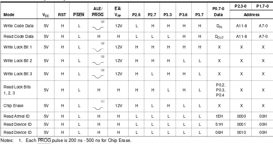
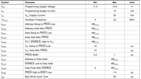
Features
• Compatible with MCS-51® Products
• 4K Bytes of In-System Programmable (ISP) Flash Memory
– Endurance: 1000 Write/Erase Cycles
• 4.0V to 5.5V Operating Range
• Fully Static Operation: 0 Hz to 33 MHz
• Three-level Program Memory Lock
• 128 x 8-bit Internal RAM
• 32 Programmable I/O Lines
• Two 16-bit Timer/Counters
• Six Interrupt Sources
• Full Duplex UART Serial Channel
• Low-power Idle and Power-down Modes
• Interrupt Recovery from Power-down Mode
• Watchdog Timer
• Dual Data Pointer
• Power-off Flag
• Fast Programming Time
• Flexible ISP Programming (Byte and Page Mode)
Description
The AT89S51 is a low-power, high-performance CMOS 8-bit microcontroller with 4K bytes of in-system programmable Flash memory. The device is manufactured using Atmel’s high-density nonvolatile memory technology and is compatible with the indus-try-standard 80C51 instruction set and pinout. The on-chip Flash allows the program memory to be reprogrammed in-system or by a conventional nonvolatile memory pro-grammer. By combining a versatile 8-bit CPU with in-system programmable Flash on a monolithic chip, the Atmel AT89S51 is a powerful microcontroller which provides a highly-flexible and cost-effective solution to many embedded control applications. The AT89S51 provides the following standard features: 4K bytes of Flash, 128 bytes of RAM, 32 I/O lines, Watchdog timer, two data pointers, two 16-bit timer/counters, a five-vector two-level interrupt architecture, a full duplex serial port, on-chip oscillator, and clock circuitry. In addition, the AT89S51 is designed with static logic for operation down to zero frequency and supports two software selectable power saving modes. The Idle Mode stops the CPU while allowing the RAM, timer/counters, serial port, and interrupt system to continue functioning. The Power-down mode saves the RAM con-tents but freezes the oscillator, disabling all other chip functions until the next external interrupt or hardware reset.
8-bit
Microcontroller
with 4K Bytes
In-System
Programmable
Flash
AT89S51
2
AT89S51
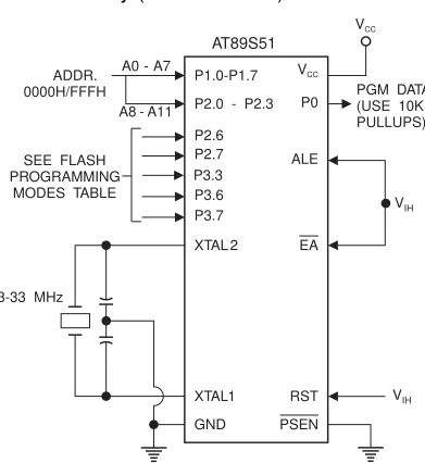
2487A–10/01Pin Configurations
PDIP TQFP 1 2 3 4 5 6 7 8 9 10 11 12 13 14 15 16 17 18 19 20 40 39 38 37 36 35 34 33 32 31 30 29 28 27 26 25 24 23 22 21 P1.0 P1.1 P1.2 P1.3 P1.4 (MOSI) P1.5 (MISO) P1.6 (SCK) P1.7 RST (RXD) P3.0 (TXD) P3.1 (INT0) P3.2 (INT1) P3.3 (T0) P3.4 (T1) P3.5 (WR) P3.6 (RD) P3.7 XTAL2 XTAL1 GND VCC P0.0 (AD0) P0.1 (AD1) P0.2 (AD2) P0.3 (AD3) P0.4 (AD4) P0.5 (AD5) P0.6 (AD6) P0.7 (AD7) EA/VPP ALE/PROG PSEN P2.7 (A15) P2.6 (A14) P2.5 (A13) P2.4 (A12) P2.3 (A11) P2.2 (A10) P2.1 (A9) P2.0 (A8) 1 2 3 4 5 6 7 8 9 10 11 33 32 31 30 29 28 27 26 25 24 23 44 43 42 41 40 39 38 37 36 35 3412 13 14 15 16 17 18 19 20 21 22 (MOSI) P1.5 (MISO) P1.6 (SCK) P1.7 RST (RXD) P3.0 NC (TXD) P3.1 (INT0) P3.2 (INT1) P3.3 (T0) P3.4 (T1) P3.5 P0.4 (AD4) P0.5 (AD5) P0.6 (AD6) P0.7 (AD7) EA/VPP NC ALE/PROG PSEN P2.7 (A15) P2.6 (A14) P2.5 (A13) P1.4 P1.3 P1.2 P1.1 P1.0 NC VCC P0.0 (AD0) P0.1 (AD1) P0.2 (AD2) P0.3 (AD3)
(WR) P3.6 (RD) P3.7
XTAL2 XTAL1 GND GND
(A8) P2.0 (A9) P2.1 (A10) P2.2 (A11) P2.3 (A12) P2.4
PLCC 7 8 9 10 11 12 13 14 15 16 17 39 38 37 36 35 34 33 32 31 30 29 (MOSI) P1.5 (MISO) P1.6 (SCK) P1.7 RST (RXD) P3.0 NC (TXD) P3.1 (INT0) P3.2 (INT1) P3.3 (T0) P3.4 (T1) P3.5 P0.4 (AD4) P0.5 (AD5) P0.6 (AD6) P0.7 (AD7) EA/VPP NC ALE/PROG PSEN P2.7 (A15) P2.6 (A14) P2.5 (A13) 6 5 4 3 2 1 44 43 42 41 40
18 19 20 21 22 23 24 25 26 27 28
(WR) P3.6 (RD) P3.7 XTAL2 XTAL1 GND
NC
3
AT89S51
2487A–10/01
Block Diagram
PORT 2 DRIVERS
PORT 2 LATCH
P2.0 - P2.7
FLASH PORT 0 LATCH RAM PROGRAM ADDRESS REGISTER BUFFER PC INCREMENTER PROGRAM COUNTER DUAL DPTR INSTRUCTION REGISTER B REGISTER
INTERRUPT, SERIAL PORT, AND TIMER BLOCKS
STACK POINTER ACC TMP2 TMP1 ALU PSW TIMING AND CONTROL
PORT 1 DRIVERS
P1.0 - P1.7 PORT 3
LATCH
PORT 3 DRIVERS
P3.0 - P3.7 OSC
GND
VCC
PSEN
ALE/PROG
EA / VPP
RST
RAM ADDR. REGISTER
PORT 0 DRIVERS P0.0 - P0.7
PORT 1 LATCH WATCH
4
AT89S51
2487A–10/01
Pin Description
VCC
Supply voltage.GND
Ground.Port 0
Port 0 is an 8-bit open drain bidirectional I/O port. As an output port, each pin can sink eightTTL inputs. When 1s are written to port 0 pins, the pins can be used as high-impedance inputs.
Port 0 can also be configured to be the multiplexed low-order address/data bus during accesses to external program and data memory. In this mode, P0 has internal pull-ups.
Port 0 also receives the code bytes during Flash programming and outputs the code bytes during program verification. External pull-ups are required during program verification.
Port 1
Port 1 is an 8-bit bidirectional I/O port with internal pull-ups. The Port 1 output buffers cansink/source four TTL inputs. When 1s are written to Port 1 pins, they are pulled high by the internal pull-ups and can be used as inputs. As inputs, Port 1 pins that are externally being pulled low will source current (IIL) because of the internal pull-ups.
Port 1 also receives the low-order address bytes during Flash programming and verification.
Port 2
Port 2 is an 8-bit bidirectional I/O port with internal pull-ups. The Port 2 output buffers cansink/source four TTL inputs. When 1s are written to Port 2 pins, they are pulled high by the internal pull-ups and can be used as inputs. As inputs, Port 2 pins that are externally being pulled low will source current (IIL) because of the internal pull-ups.
Port 2 emits the high-order address byte during fetches from external program memory and during accesses to external data memory that use 16-bit addresses (MOVX @ DPTR). In this application, Port 2 uses strong internal pull-ups when emitting 1s. During accesses to external data memory that use 8-bit addresses (MOVX @ RI), Port 2 emits the contents of the P2 Spe-cial Function Register.
Port 2 also receives the high-order address bits and some control signals during Flash pro-gramming and verification.
Port 3
Port 3 is an 8-bit bidirectional I/O port with internal pull-ups. The Port 3 output buffers cansink/source four TTL inputs. When 1s are written to Port 3 pins, they are pulled high by the internal pull-ups and can be used as inputs. As inputs, Port 3 pins that are externally being pulled low will source current (IIL) because of the pull-ups.
Port 3 receives some control signals for Flash programming and verification.
Port 3 also serves the functions of various special features of the AT89S51, as shown in the following table.
Port Pin Alternate Functions
P1.5 MOSI (used for In-System Programming)
P1.6 MISO (used for In-System Programming)
5
AT89S51
2487A–10/01
RST
Reset input. A high on this pin for two machine cycles while the oscillator is running resets thedevice. This pin drives High for 98 oscillator periods after the Watchdog times out. The DIS-RTO bit in SFR AUXR (address 8EH) can be used to disable this feature. In the default state of bit DISRTO, the RESET HIGH out feature is enabled.
ALE/PROG
Address Latch Enable (ALE) is an output pulse for latching the low byte of the address duringaccesses to external memory. This pin is also the program pulse input (PROG) during Flash programming.
In normal operation, ALE is emitted at a constant rate of 1/6 the oscillator frequency and may be used for external timing or clocking purposes. Note, however, that one ALE pulse is skipped during each access to external data memory.
If desired, ALE operation can be disabled by setting bit 0 of SFR location 8EH. With the bit set, ALE is active only during a MOVX or MOVC instruction. Otherwise, the pin is weakly pulled high. Setting the ALE-disable bit has no effect if the microcontroller is in external execution mode.
PSEN
Program Store Enable (PSEN) is the read strobe to external program memory.When the AT89S51 is executing code from external program memory, PSEN is activated twice each machine cycle, except that two PSEN activations are skipped during each access to external data memory.
EA/VPP
External Access Enable. EA must be strapped to GND in order to enable the device to fetchcode from external program memory locations starting at 0000H up to FFFFH. Note, however, that if lock bit 1 is programmed, EA will be internally latched on reset.
EA should be strapped to VCC for internal program executions.
This pin also receives the 12-volt programming enable voltage (VPP) during Flash programming.
XTAL1
Input to the inverting oscillator amplifier and input to the internal clock operating circuit.XTAL2
Output from the inverting oscillator amplifierPort Pin Alternate Functions
P3.0 RXD (serial input port)
P3.1 TXD (serial output port)
P3.2 INT0 (external interrupt 0)
P3.3 INT1 (external interrupt 1)
P3.4 T0 (timer 0 external input)
P3.5 T1 (timer 1 external input)
P3.6 WR (external data memory write strobe)
6
AT89S51
2487A–10/01
Special
Function
Registers
A map of the on-chip memory area called the Special Function Register (SFR) space is shown in Table 1.
Note that not all of the addresses are occupied, and unoccupied addresses may not be imple-mented on the chip. Read accesses to these addresses will in general return random data, and write accesses will have an indeterminate effect.
Table 1. AT89S51 SFR Map and Reset Values
7
AT89S51
2487A–10/01
User software should not write 1s to these unlisted locations, since they may be used in future products to invoke new features. In that case, the reset or inactive values of the new bits will always be 0.
Interrupt Registers: The individual interrupt enable bits are in the IE register. Two priorities can be set for each of the five interrupt sources in the IP register.
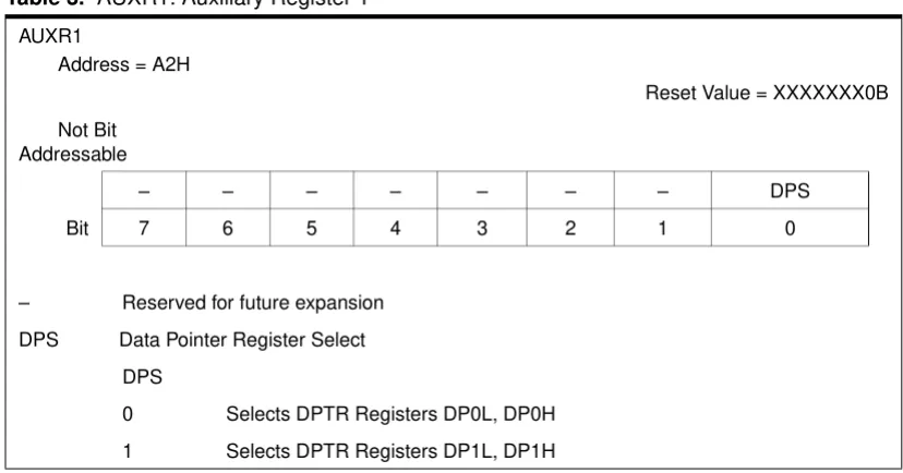
Dual Data Pointer Registers: To facilitate accessing both internal and external data memory, two banks of 16-bit Data Pointer Registers are provided: DP0 at SFR address locations 82H-83H and DP1 at 84H-85H. Bit DPS = 0 in SFR AUXR1 selects DP0 and DPS = 1 selects DP1. The user should always initialize the DPS bit to the appropriate value before accessing the respective Data Pointer Register.
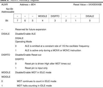
Table 2. AUXR: Auxiliary Register
AUXR Address = 8EH Reset Value = XXX00XX0B
Not Bit Addressable
– – – WDIDLE DISRTO – – DISALE
Bit 7 6 5 4 3 2 1 0
– Reserved for future expansion
DISALE Disable/Enable ALE
DISALE Operating Mode
0 ALE is emitted at a constant rate of 1/6 the oscillator frequency
1 ALE is active only during a MOVX or MOVC instruction
DISRTO Disable/Enable Reset out
DISRTO
0 Reset pin is driven High after WDT times out
1 Reset pin is input only
WDIDLE Disable/Enable WDT in IDLE mode
WDIDLE
0 WDT continues to count in IDLE mode
8
AT89S51
2487A–10/01
Power Off Flag: The Power Off Flag (POF) is located at bit 4 (PCON.4) in the PCON SFR. POF is set to “1” during power up. It can be set and rest under software control and is not affected by reset.
Memory
Organization
MCS-51 devices have a separate address space for Program and Data Memory. Up to 64K bytes each of external Program and Data Memory can be addressed.
Program Memory
If the EA pin is connected to GND, all program fetches are directed to external memory.On the AT89S51, if EA is connected to VCC, program fetches to addresses 0000H through FFFH are directed to internal memory and fetches to addresses 1000H through FFFFH are directed to external memory.
Data Memory
The AT89S51 implements 128 bytes of on-chip RAM. The 128 bytes are accessible via directand indirect addressing modes. Stack operations are examples of indirect addressing, so the 128 bytes of data RAM are available as stack space.
Watchdog
Timer
(One-time
Enabled with
Reset-out)
The WDT is intended as a recovery method in situations where the CPU may be subjected to software upsets. The WDT consists of a 14-bit counter and the Watchdog Timer Reset (WDTRST) SFR. The WDT is defaulted to disable from exiting reset. To enable the WDT, a user must write 01EH and 0E1H in sequence to the WDTRST register (SFR location 0A6H). When the WDT is enabled, it will increment every machine cycle while the oscillator is running. The WDT timeout period is dependent on the external clock frequency. There is no way to dis-able the WDT except through reset (either hardware reset or WDT overflow reset). When WDT overflows, it will drive an output RESET HIGH pulse at the RST pin.
Using the WDT
To enable the WDT, a user must write 01EH and 0E1H in sequence to the WDTRST register (SFR location 0A6H). When the WDT is enabled, the user needs to service it by writing 01EH and 0E1H to WDTRST to avoid a WDT overflow. The 14-bit counter overflows when it reaches 16383 (3FFFH), and this will reset the device. When the WDT is enabled, it will increment every machine cycle while the oscillator is running. This means the user must reset the WDT at least every 16383 machine cycles. To reset the WDT the user must write 01EH and 0E1H to WDTRST. WDTRST is a write-only register. The WDT counter cannot be read or written. When WDT overflows, it will generate an output RESET pulse at the RST pin. The RESET pulse duration is 98xTOSC, where TOSC=1/FOSC. To make the best use of the WDT, itTable 3. AUXR1: Auxiliary Register 1
AUXR1
Address = A2H
Reset Value = XXXXXXX0B
Not Bit Addressable
– – – – – – – DPS
Bit 7 6 5 4 3 2 1 0
– Reserved for future expansion
DPS Data Pointer Register Select
DPS
0 Selects DPTR Registers DP0L, DP0H
9
AT89S51
2487A–10/01
should be serviced in those sections of code that will periodically be executed within the time required to prevent a WDT reset.
WDT During
Power-down
and Idle
In down mode the oscillator stops, which means the WDT also stops. While in Power-down mode, the user does not need to service the WDT. There are two methods of exiting Power-down mode: by a hardware reset or via a level-activated external interrupt, which is enabled prior to entering Power-down mode. When Power-down is exited with hardware reset, servicing the WDT should occur as it normally does whenever the AT89S51 is reset. Exiting Power-down with an interrupt is significantly different. The interrupt is held low long enough for the oscillator to stabilize. When the interrupt is brought high, the interrupt is serviced. To pre-vent the WDT from resetting the device while the interrupt pin is held low, the WDT is not started until the interrupt is pulled high. It is suggested that the WDT be reset during the inter-rupt service for the interinter-rupt used to exit Power-down mode.
To ensure that the WDT does not overflow within a few states of exiting Power-down, it is best to reset the WDT just before entering Power-down mode.
Before going into the IDLE mode, the WDIDLE bit in SFR AUXR is used to determine whether the WDT continues to count if enabled. The WDT keeps counting during IDLE (WDIDLE bit = 0) as the default state. To prevent the WDT from resetting the AT89S51 while in IDLE mode, the user should always set up a timer that will periodically exit IDLE, service the WDT, and reenter IDLE mode.
With WDIDLE bit enabled, the WDT will stop to count in IDLE mode and resumes the count upon exit from IDLE.
UART
The UART in the AT89S51 operates the same way as the UART in the AT89C51. For furtherinformation on the UART operation, refer to the ATMEL Web site (http://www.atmel.com). From the home page, select ‘Products’, then ‘8051-Architecture Flash Microcontroller’, then ‘Product Overview’.
Timer 0 and 1
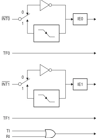
Timer 0 and Timer 1 in the AT89S51 operate the same way as Timer 0 and Timer 1 in the AT89C51. For further information on the timers’ operation, refer to the ATMEL Web site (http://www.atmel.com). From the home page, select ‘Products’, then ‘8051-Architecture Flash Microcontroller’, then ‘Product Overview’.Interrupts
The AT89S51 has a total of five interrupt vectors: two external interrupts (INT0 and INT1), two timer interrupts (Timers 0 and 1), and the serial port interrupt. These interrupts are all shown in Figure 1.Each of these interrupt sources can be individually enabled or disabled by setting or clearing a bit in Special Function Register IE. IE also contains a global disable bit, EA, which disables all interrupts at once.
Note that Table 4 shows that bit position IE.6 is unimplemented. In the AT89S51, bit position IE.5 is also unimplemented. User software should not write 1s to these bit positions, since they may be used in future AT89 products.
10
AT89S51
2487A–10/01
.
Figure 1. Interrupt Sources
Table 4. Interrupt Enable (IE) Register
(MSB) (LSB)
EA – – ES ET1 EX1 ET0 EX0
Enable Bit = 1 enables the interrupt.
Enable Bit = 0 disables the interrupt.
Symbol Position Function
EA IE.7 Disables all interrupts. If EA = 0, no interrupt is
acknowledged. If EA = 1, each interrupt source is individually enabled or disabled by setting or clearing its enable bit.
– IE.6 Reserved
– IE.5 Reserved
ES IE.4 Serial Port interrupt enable bit
ET1 IE.3 Timer 1 interrupt enable bit
EX1 IE.2 External interrupt 1 enable bit
ET0 IE.1 Timer 0 interrupt enable bit
EX0 IE.0 External interrupt 0 enable bit
User software should never write 1s to reserved bits, because they may be used in future AT89 products.
IE1 IE0
1 1
0 0
TF1 TF0
INT1 INT0
11
AT89S51
2487A–10/01
Oscillator
Characteristics
XTAL1 and XTAL2 are the input and output, respectively, of an inverting amplifier that can be configured for use as an on-chip oscillator, as shown in Figure 2. Either a quartz crystal or ceramic resonator may be used. To drive the device from an external clock source, XTAL2 should be left unconnected while XTAL1 is driven, as shown in Figure 3. There are no require-ments on the duty cycle of the external clock signal, since the input to the internal clocking circuitry is through a divide-by-two flip-flop, but minimum and maximum voltage high and low time specifications must be observed.
Figure 2. Oscillato