M2 S2
P.Gargini
Attacking the Red Brick Walls of the
International Technology Roadmap
for Semiconductors
(ITRS)
Dr. Paolo Gargini
Chairman ITRS
2001 Edition
M2 S2
P.Gargini
What is the ITRS?
• A consensus reference document with a 15
year outlook on the requirements of the
semiconductor industry
– Provides a
reference
document for Equipment,
Materials and Software
Suppliers
on the
Needs
of the
Semiconductor Industry and on
Possible Solutions
M2 S2
P.Gargini
Technology Hierarchy
•
Technology Needs
•
Possible Solutions
•
Detailed Solutions
•
Implementation
Example:
•
Reduce Signal Propagation Delay of
Interconnections
•
Metal Potential Solution: Cu Metal
Dielectric Potential Solution: Low K
Dielectric
•
Use: Cu CVD Seed Layer + Cu
Plating+ CMP+Low K CVD
•
Establish Supplier Infrastructure
Tech
nol
ogy
Ro
adm
ap
Do
ma
in
Tech
nol
ogy
Im
ple
me
nta
tion
Do
ma
M2 S2
P.Gargini
Roadmap Editions
Japan
Korea
Europe
Taiwan
USA
2002ITRS
Update
2001ITRS
2000ITRS
Update
1999ITRS
1998ITRS
Update
1997NTRS
1994NTRS
1992NTRS
http://public.itrs.net
2001 Edition
1991
M2 S2
P.Gargini
P. Gargini
International and Domestic Timing
Domestic
Domestic
3Q
USA
Europe
2Q
1Q
Domestic
Domestic
Region A
Region B
Time
4Q
Korea
Japan
Taiwan
1999, 2002
2000
2001
M2 S2
P.Gargini
M2 S2
P.Gargini
Mission of ITRS
IRC
Technology Needs
Potential Solutions
in
near & long term
ITWG
ITWG
•
Policy
•
Goals
•
Schedule
•
Coordination
among ITWGs
•
Coordination
among
Associations
TWG
TWG
TWG
TWG
TWG
ESIA
KSIA
SIA
TSIA
JEITA
(STRJ)
Design
Test
M2 S2
P.Gargini
International Technology Working
Groups
• Assembly & Packaging
• Design
• Factory Integration
• Front End Process
• Interconnect
• Lithography
• PIDS, Emerging Devices
• Test
ITWG
• Environment, Safety,
Health
• Metrology
• Modeling and Simulation
• Yield Enhancement
Cross ITWG
M2 S2
P.Gargini
2001 Edition
ITRS Framework
Factory Integration
Yield Enhancement
QFP
BGA
PGA
Printed Wiring Board
Assembly
Test
Wells
Source / Drain
- Extension
Isolation
Channel
Contacts
FEP
Lithography
PIDS
Metrology Modeling
Starting Material
Interconnect
Design
M2 S2
P.Gargini
Chapters of ITRS 2001
Glossary
ORTC
12 ITWGs : Design to Modeling & Simulation
- Scope
- Difficult Challenges
- Technology Requirement
- Potential Solutions
System Drivers
Difficult Challenges
Grand Challenges
Introduction
M2 S2
P.Gargini
Contact Information for the ITRS
¾
For general questions or information regarding ITRS publications and
public forums visit the ITRS web site
http://public.itrs.net
[
note that
there is no “www” in our web site address
.].
To order a Roadmap through email, use the ITRS email address
or access the ITRS web site.
¾
Other questions or comments?
call
Linda Wilson
ITRS Information Manager
512.356.3605
Sarah Mangum
ITRS Webmaster
512.356.3558
2001 ITRS Book and CD sales
•
$25 for CDs, $35 for CDs shipped outside the U.S.A
•
$50 for Books, $65 for ITRS books shipped outside the U.S.A.
M2 S2
P.Gargini
Composition of the Technology
Working Group (ITWG) in 2001
TWG Members by Regions
TWG Members by Affiliations
23%
54%
22%
Consortia /
Research Inst. /
University
193
Equipment /
Materials
Suppliers 185
Chip Makers
445
1%
Other
10
Europe
68
Taiwan
161
8%
19%
8%
Korea
64
Japan
222
USA
324
M2 S2
P.Gargini
DuPont Company
Silicon Valley Group, Inc
ION Systems
M+W Zandar
Nanya Technology Co.
Compaq Computer Corp
Asyst Technologies, Inc.
Sumitomo Sitix Corp.
Varian
Air Products & Chemicals
Etec Systems, Inc.
n-Line Corporation
K&S
Applied Materials
KLA-Tencor
Tokyo Electron America
SEMI
Novellus Systems
Wacker Siltronic Corp.
Agilent Technologies
Winbond Electronics Corp.
Axcelis Technologies, Inc.
Komatsu Silicon
MEMC
Canon Inc.
CamLine
Ebara
Rohm
Sanyo
FSI International
Genus
Ibis Technology
Okmetic Ltd.
SiGen
Soitec
Tokin Corp
BOC Edwards
Nortel Networks
Cadence
Intransa
UBC
ATMI
Cabot Corporation
E4 Technologies
Praxair, Inc.
SONY
URS Corporation
Dow Chemical
Micronix
ASM Lithography
Nikon Corporation
Photronics, Inc.
Shipley Company, Inc.
Episil Technologies
Metrology Edge
Therma-Wave
Oki Electric Ind. Co., Ltd.
M2 S2
P.Gargini
DETAILED SOLUTIONS
And
M2 S2
P.Gargini
From Strategy to Implementation
From Strategy to Implementation
Technology Needs
Possible Solutions
ITRS
Implementation
Suppliers
IC Makers
OEM
Suppliers
Consortia
M2 S2
P.Gargini
Use of ITRS as a Global Planning Tool
Use of ITRS as a Global Planning Tool
Internal
Internal
R&D
R&D
Consortia
Consortia
Suppliers
Suppliers
External
External
R&D
R&D
SRC
Natl Lab
ISMT
IMEC
LETI
MEDEA
MIRAI
ASET
M2 S2
P.Gargini
PR
JR
i
Consortia Locations
IRAI
IRAI
M2 S2
P.Gargini
M2 S2
P.Gargini
R
R
®
®
'68 '70
'72 '74
'76 '78
'80 '82
'84 '86
'88 '90
'92 '94
'96 '98
'00 '02
10
17
10
16
10
15
10
14
10
13
10
12
10
11
10
10
10
9
Units
Source: WSTS/Dataquest/Intel, 8/02
Source: WSTS/Dataquest/Intel, 8/02
10
18
Transistors Shipped per
Transistors Shipped per
Year
M2 S2
P.Gargini
Worldwide Semiconductor
R
R
®
®
1
10
100
1000
'68 ’70 '72 '74 '76 '78 '80 '82 '84 '86 '88 ’90 '92 '94 '96 '98 '00 '02
1
10
100
1000
'68 ’70 '72 '74 '76 '78 '80 '82 '84 '86 '88 ’90 '92 '94 '96 '98 '00 '02
$B
$B
Source: Intel/WSTS, 8/02
Source: Intel/WSTS, 8/02
Worldwide Semiconductor
Revenues
M2 S2
P.Gargini
R
R
®
®
Average Transistor Price
Average Transistor Price
by Year
by Year
0.0000001
0.000001
0.00001
0.0001
0.001
0.01
0.1
1
10
'68 '70 '72 '74 '76 '78 '80 '82 '84 '86 '88 '90 '92 '94 '96 '98 '00 '02
$
$
Source: WSTS/Dataquest/Intel, 8/02
M2 S2
P.Gargini
ITRS GUIDING PRINCIPLE
50% TRANSISTOR AREA READUCION
GENERATION TO GENERATION
50%
M2 S2
P.Gargini
Pentium
®
Processor
Pentium
®
Pro
Processor
Pentium
®
II
Processor
Pentium
®
III
Processor
Pentium
®
4
Processor
0.8µ
0.6µ
0.35µ
0.25µ
0.18µ
0.13µ
Intel’s Process Technology
Basic Feature Size in microns
M2 S2
P.Gargini
DEFINITIONS
And
M2 S2
P.Gargini
Technology Node Definition
One half of the smallest pitch in the technology,
Typically represented by the first metal layer
M2 S2
P.Gargini
Half Pitch (=Pitch/2) Definition
(Typical
DRAM)
Metal
Pitch
(Typical
MPU/ASIC)
Poly
M2 S2
P.Gargini
MOS Transistor
Scaling
(1974 to present)
S=0.7
[0.5x per 2 nodes]
M2 S2
P.Gargini
ITRS
ITRS
P.Gargini
10
1994 NTRS Roadmap
Year: 95 96 97 98 99 00 01 02 03 04 05 06 07
1/2 pitch* 350 250 180 130
100
*
Dimensions for minimum half pitch and isolated line in nm
Source: National Technology Roadmap for Semiconductors
M2 S2
P.Gargini
100
70
50
35
25
WAS
IS
91
64
45
31
22
X
130
0.7
90
0.7
65
0.7
45
0.7
32
0.7
90
65
45
32
22
Actual
Technology Nodes (nm)
M2 S2
P.Gargini
1999 ITRS Timing
Year of Production
2001
2002
2003
2004
2005
2006
2007
DRAM ½ Pitch
130
115
100
90
80
70
65
MPU/ASIC ½ Pitch
150
130
107
90
80
70
65
MPU Pr Gate Length
90
75
53
45
40
35
MPU Ph Gate Length
53
45
37
32
28
25
65
65
MPU Pr Gate Length
1999
180
2000 2001
2002
130
2003 2004
2005
100
DRAM ½ Pitch (nm)
165 150
120 110
MPU Gate Length (nm)
140
120
85-90
80
MPU / ASIC ½ Pitch (nm)
230
210
180
160
145
130
115
ASIC Gate Length (nm)
180
165
150
130
120
110
100
180
130
100
100
70
65
65
100
Year of Production
2001 ITRS Timing
-1
-2
-4
M2 S2
P.Gargini
Production Ramp-up Model and Technology Node
Volume (Parts/Month)
1K
10K
100K
Months
0
-24
1M
10M
100M
Alpha
Tool
12
24
-12
Development
Production
Beta
Tool
Production
Tool
First
Conf.
Papers
First Two
Companies
Reaching
Production
2
Volume (Wafers/Month)
20
200
2K
20K
200K
M2 S2
P.Gargini
Innovation
1.4X
Technology
2X
Manufacturing
1.4X
3-year cycle
(1977~1995)
M2 S2
P.Gargini
1980
1990
2000
2010
2020
100
1000
10,000
10
DRAM Chip Size Trend
38mm
2
75mm
2
150mm
2
300mm
2
1.4X/3-years
1M
1G
1T
~2
~2
X die growth in 6 years
X die growth in 6 years
Ch
ip
S
iz
e
(m
m
2
)
Max Litho Field
(4X)
M2 S2
P.Gargini
Innovation
1.4X
Technology
2X
Manufacturing
1.4X
3-year -> 2-year cycle
(~1995-2010)
3-year cycle
4X/3 Years
1.4X
->
1.0X
M2 S2
P.Gargini
1980
1990
2000
2010
2020
100
1000
10,000
10
DRAM Chip Size Trend
38mm
2
75mm
2
150mm
2
300mm
2
800mm
2
1.4X/3-years
1M
1G
1T
~2
~2
X die growth in 6 years
X die growth in 6 years
Ch
ip
S
iz
e
(m
m
M2 S2
P.Gargini
TABLES
And
M2 S2
P.Gargini
Table’s Structure
• All tables are divided in two parts:
–
Near Term
• Six year outlook (e.g., 2001-2007)
• All values are reported on a yearly basis
–
Long Term
M2 S2
P.Gargini
Tables’ Color Scheme
• A new category will be introduced starting with
2002ITRS Update
Solutions Exist
White
Yellow
Solutions Being Pursued
No Known Solutions
M2 S2
P.Gargini
YEAR
TECHNOLOGY NODE
2008 70 nm 2011 50 nm 2014 35 nm DRIVER
[1] DRAM ½ Pitch (nm) 70 50 35
[2] MPU Ga t e Lengt h (nm) 45 32 22
[3] MPU / ASIC ½ Pitch (nm) 80 55 40
[4] ASIC Ga t e Lengt h (nm) 70 50 35
[5] Minimum logic Vdd (V) (desktop) 0.6–0.9 0.5–0.6 0.3–0.6 M Gate
[6] Tox equivalent (nm) 0.8–1.2 0.6–0.8 0.5–0.6 M Gate [7] Nominal I
on at 25 °C (µA/µm) [NMOS/PMOS]
high performance
750/350 750/350 750/350 M Gate [8] Maximum Ioff at 25 °C (nA/µm)
(For minimum L device) high-performance
40 80 160 M Gate [9] Gate delay metric CV/I (ps) high-performance 3.7 2.6 2.4
[10]Percent static power reduction necessary due to innovative circuit/system design
91 97 98 M Gate M & A ½ [11]Nominal I
on at 25 °C (µA/µm) [NMOS/PMOS] low power
490/230 490/230 490/230 A Gate [12]Maximum I
off at 25 °C (pA/µm) (For minimum L device) low power
40 80 160 A Gate [13]Gate delay metric CV/I (ps) low power 5.6 4.5 3.7
[14]Percent static power reduction necessary due to innovative circuit/system design
95 98 99 A Gate M & A ½ [15]VT 3s variation (±mV) (For minimum L device) 25 17 17 M Gate
[16]S/D extension junction depth, nominal (µm) 0.02–0.028 0.013–0.02 0.01–0.014 M Gate
Work in Progress -- - Not for Publication
Interconnect/7-8-99/CCase
DRAM Long Term Requirements
Y
EAR OFI
NTRO DUCTION“
TE CHNOLOGY NODE”
2 008
70 nm
2 011
50 nm
2 014
35 nm
DRAM pitch
70
50
35
Number of metal levels
4
4
4
Contact A/R – stacked capacitor
10.5
12
13.5
Lo cal wiring pitch (nm) non-contacted
140
100
70
Specific co ntact resistance (
Ω
-cm
2)
8 E-8
3 E-8
2 E-8
Specific via resistance (
Ω
-cm
2)
6E-10
3E-10
1.5E-10
Metal effective resistivity (
µΩ
-cm)
2.2
2.2
2.2
Interlevel metal insulator - effective dielectric constant (k)
2.5 - 3.0
2.0 - 2.5
2.0 - 2.3
Solutions Exist Solutions B eing Pursue d No Known Solutions
No Known Solutions to A/R
High
κ
materials may provide some relief
Table 28a Memory and Logic Technology Requirements—Near Term
Y
EART
ECHNOLOGYN
ODE1999
180 nm
2000 2001
2002
130 nm
2003 2004
2005
100 nm
D
RIVER1
DRAM ½ Pitch (nm)
180
165
150
130
120
110
100
2
MPU Gate Length (nm)
140
120
100
85
80
70
65
3
MPU / ASIC ½ (nm)
230
210
180
160
145
130
115
4
ASIC Gate Length (nm)
180
165
150
130
120
110
100
5 Minimum logic V
dd (V) (desktop)
1.5–1.8 1.5–1.8 1.2–1.5 1.2–1.5 1.2–1.5 0.9–1.2 0.9–1.2M GATE
6 Tox equivalent (nm) 1.9–2.5 1.9–2.5 1.5–1.9 1.5–1.9 1.5–1.9 1.2–1.51.0–1.5M GATE
7 Nominal Ion at 25 °C (µA/µm) [NMOS/PMOS] high-performance
750/350 750/35 0
750/350 750/350 750/35 0
750/350 750/350M GATE
8 Maximum Ioff at 25 °C (nA/µm) (For minimum L device) high performance
5 7 8 10 13 16 20 M GATE
9 Gate delay metric CV/I (ps) high-performance 11 9.4 8.6 7.3 6.9 6.1 5.7
10Percent static power reduction necessary due to innovative circuit/system design
0
33 48 55 71 77 81
M GATE
M & A ½ 11Nominal Ion at 25 °C (µA/µm)
[NMOS/PMOS] low power
490/230 490/23 0
490/230 490/230 490/23 0
490/230 490/230A GATE
12Maximum I
off at 25 °C (pA/µm)
(For minimum L device) low power
5 7 8 10 13 16 20 A GATE
13Gate delay metric CV/I (ps) low power 18 16 13 11.2 10.7 8.8 8.2
14Percent static power reduction necessary due to innovative circuit/system design
0 36 55 65 80 85 88 A GATE
M & A ½ 15VT 3σ variation (±mV)
(For minimum L device)
50 50 42 42 42 33 33 M GATE
16S/D extension junction depth, nominal (µm) 0.045– 0.07 0.04 – 0.065 0.04– 0.06 0.03–0.05 0.03– 0.048 0.028– 0.044 0.025– 0.04 M GATE
Solutions Exist Solutions Being Pursued No Known Solutions
Table 46b MPU Interconnect Technology Requirements—Long Term
Y
EART
ECHNOLOGYN
ODE2008
70 nm
2011
50 nm
2014
35 nm
MPU ½ pitch
80
55
40
MPU gate length (nm)
45
32
22
Number of metal levels 9 9–10 10
Number of optional levels – ground planes/capacitors 3 4 4
Jmax (A/cm2
)—wire (at 105°C) 2.1E6 3.7E6 4.6E6
Imax (mA)—via (at 105°C) 0.18 0.16 0.11
Local wiring pitch (nm) 185 130 95
Local A/R (for Cu) 1.9 2.1 2.3
Cu local dishing (nm), 5% × height 9 7 5
Intermediate wiring pitch (nm) 240 165 115
Intermediate wiring dual damascene A/R (Cu wire/via) 2.5/2.3 2.7/2.4 2.9/2.5
Cu intermediate wiring dishing (nm), 15 micron wide wire, 10% × height
30 22 17
Dielectric erosion (nm), intermediate wiring 0 0 0
Minimum global wiring pitch (nm) 390 275 190
Global wiring dual damascene A/R (Cu wire/via) 2.8/2.9 2.9/3.0 3.0/3.1
Cu global wiring dishing (nm), 15 micron wide wire, 10% × height
55 38 29
Conductor effective resistivity (µΩ-cm) Cu wiring 1.8 <1.8 <1.8
Barrier/cladding thickness (nm) 0 0 0
Interlevel metal insulator—effective dielectric constant (κ) 1.5 <1.5 <1.5
Solutions Exist Solutions Being Pursued No Known Solutions
DRAM interconnect technology
Table 46a MPU Interconnect Technology Requirements—Near Term
YEAR
TECHNOLOGY NODE
1999 180 nm
2000 2001 2002 130 nm
2003 2004 200 100
MPU ½ pitch 230 210 180 160 145 130 11
MPU gate length (nm) 140 120 100 85 80 70 65
Number of metal levels 6-7 6–7 7 7–8 8 8 8–
Number of optional levels— ground planes/capacitors
0 0 0 2 2 2 2
Jmax (A/cm2
)—wire (at 105°C) 5.8E5 7.1E5 8.0E5 9.6E5 1.1E6 1.3E6 1.4
Imax (mA)—via (at 105°C) 0.36 0.36 0.33 0.32 0.29 0.27 0.2
Local wiring pitch (nm) 500 450 405 365 330 295 26
Local wiring A/R (for Al) 2 2 2.1 2.1 2.2 ** **
Local wiring A/R (for Cu) 1.4 1.4 1.5 1.5 1.6 1.6 1.
Cu local dishing (nm), 5% × height 18 16 15 14 13 12 11
Intermediate wiring pitch (nm) 640 575 520 465 420 375 34
Intermediate wiring A/R (Al) 2.2 2.3 2.4 2.5 2.6 ** **
Intermediate wiring dual damascene A/R (Cu wire/via)
2.0/2.1 2.1/2.1 2.2/2.1 2.2/2.1 2.2/2.2 2.3/2.2 2.4/
Cu intermediate dishing (nm), 15 micron wide wire, 10% × height
64 60 57 51 46 43 41
Dielectric erosion (nm), intermediate wiring, 50% areal density, 10% × height
64 60 57 51 46 43 41
Minimum global wiring pitch (nm) 1050 945 850 765 690 620 56
Global wiring A/R (Al) 2 2.1 2.2 2.3 2.4 ** **
Global wiring dual damascene A/R (Cu wire/via)
2.2/2.4 2.3/2.6 2.4/2.7 2.5/2.7 2.6/2.8 2.7/2.8 2.7/
Cu global wiring dishing (nm), 15 micron wide wire, 10% × height
116 109 102 95 90 84 76
Conductor effective resistivity (µΩ-cm) Al wiring
3.3 3.3 3.3 3.3 3.3 ** **
Conductor effective resistivity (µΩ-cm) Cu wiring*
2.2 2.2 2.2 2.2 2.2 2.2 2.
Barrier/cladding thickness (for Cu wiring) (nm)***
17 16 14 13 12 11 10
Interlevel metal insulator —effective dielectric constant (κ)
3.5–4.0 3.5–4.0 2.7–3.5 2.7–3.5 2.2–2.7 2.2–2.7 1.6–
* Assumes a conformal barrier/ nucleation layer ** This technology is not expected to extend to this node
*** Calculated for a conformal layer in local wiring to meet minimum effective conductor resistivity
Solutions Exist Solutions Being Pursued No Known Solutions
Work in Progress --- Not for Publ ication
Interconnect/7-8-99/CCase
DRAM Short Term Requirements
YEA R OF INTRODUCTION “TECHNOLOGY NODE”
199 9 180 nm
200 0 2001 2002 130 nm
2003 2004 200 5 100 nm
DRAM p itch 18 0 16 5 15 0 13 0 12 0 11 0 10 0 Number of metal levels 3 3 3 3-4 4 4 4 Contact A/R – s tacked
capacitor
6.3 6.7 7.1 7.5 8.0 8.5 9.0
Local wiring pitch (nm) non-co ntacted
36 0 33 0 30 0 26 0 24 0 21 0 20 0
Specific co ntact resistance (Ω-cm2
)
6E-7 3E-7 2E-7
Specific via resistance (Ω-cm2
)
7E-9 2E-9 1E-9
Metal effective resistivity (µΩ-cm)
3.3 3.3 3.3 3.3 3.3 3.3 2.2
Interlevel metal insulator -effective dielectric cons tant (κ)
4.1 4.1 4.1 3. 0 - 4.1 3. 0 - 4.1 3. 0 - 4.1 2. 5 - 3.0
Solutions Exist Solutions Being Pursue d No Known Solutions
Table 28a Memory and Logic Technology Requirements—Near Term
Y
EART
ECHNOLOGYN
ODE1999
180 nm
2000 2001
2002
130 nm
2003 2004
2005
100 nm
D
RIVER1
DRAM ½ Pitch (nm)
180
165
150
130
120
110
100
2
MPU Gate Length (nm)
140
120
100
85
80
70
65
3
MPU / ASIC ½ (nm)
230
210
180
160
145
130
115
4
ASIC Gate Length (nm)
180
165
150
130
120
110
100
5Minimum logic V
dd (V) (desktop)
1.5–1.8 1.5–1.8 1.2–1.5 1.2–1.5 1.2–1.5 0.9–1.2 0.9–1.2M GATE
6Tox equivalent (nm) 1.9–2.5 1.9–2.5 1.5–1.9 1.5–1.9 1.5–1.9 1.2–1.5 1.0–1.5M GATE
7Nominal Ion at 25 °C (µA/µm) [NMOS/PMOS] high-performance
750/350 750/35 0
750/350 750/350 750/35 0
750/350 750/350M GATE
8Maximum Ioff at 25 °C (nA/µm) (For minimum L device) high performance
5 7 8 10 13 16 20 M GATE
9 Gate delay metric CV/I (ps) high-performance 11 9.4 8.6 7.3 6.9 6.1 5.7
10Percent static power reduction necessary due to innovative circuit/system design
0
33 48 55 71 77 81
M GATE
M & A ½ 11Nominal Ion at 25 °C (µA/µm)
[NMOS/PMOS] low power
490/230 490/23 0
490/230 490/230 490/23 0
490/230 490/230A GATE
12Maximum I
off at 25 °C (pA/µm)
(For minimum L device) low power
5 7 8 10 13 16 20 A GATE
13Gate delay metric CV/I (ps) low power 18 16 13 11.2 10.7 8.8 8.2
14Percent static power reduction necessary due to innovative circuit/system design
0 36 55 65 80 85 88 A GATE
M & A ½ 15VT 3σ variation (±mV)
(For minimum L device)
50 50 42 42 42 33 33 M GATE
16S/D extension junction depth, nominal (µm) 0.045– 0.07 0.04 – 0.065 0.04– 0.06 0.03–0.05 0.03– 0.048 0.028– 0.044 0.025– 0.04 M GATE
Solutions Exist Solutions Being Pursued No Known Solutions
YEAR
TECHNOLOGY NODE
2008 70 nm 2011 50 nm 2014 35 nm DRIVER
[1] DRAM ½ Pitch (nm) 70 50 35
[2] MPU Gat e Lengt h (nm) 45 32 22
[3] MPU / ASIC ½ Pitch (nm) 80 55 40
[4] ASIC Gat e Lengt h (nm) 70 50 35
[5] Minimum logic Vdd (V) (desktop) 0.6–0.9 0.5–0.6 0.3–0.6 M Gate
[6] Tox equivalent (nm) 0.8–1.2 0.6–0.8 0.5–0.6 M Gate [7] Nominal Ion at 25 °C (µA/µm) [NMOS/PMOS]
high performance
750/350 750/350 750/350 M Gate [8] Maximum Ioff at 25 °C (nA/µm)
(For minimum L device) high-performance
40 80 160 M Gate [9] Gate delay metric CV/I (ps) high-performance 3.7 2.6 2.4
[10]Percent static power reduction necessary due to innovative circuit/system design
91 97 98 M Gate M & A ½ [11]Nominal Ion at 25 °C (µA/µm) [NMOS/PMOS] low
power
490/230 490/230 490/230 A Gate [12]Maximum Ioff at 25 °C (pA/µm)
(For minimum L device) low power
40 80 160 A Gate [13]Gate delay metric CV/I (ps) low power 5.6 4.5 3.7
[14]Percent static power reduction necessary due to innovative circuit/system design
95 98 99 A Gate M & A ½ [15]VT 3s variation (±mV) (For minimum L device) 25 17 17 M Gate
[16]S/D extension junction depth, nominal (µm) 0.02–0.028 0.013–0.02 0.01–0.014 M Gate
Table 46a MPU Interconnect Technology Requirements—Near Term
YEAR
TECHNOLOGY NODE
1999 180 nm
2000 2001 2002 130 nm
2003 2004 200 100
MPU ½ pitch 230 210 180 160 145 130 11
MPU gate length (nm) 140 120 100 85 80 70 65
Number of metal levels 6-7 6–7 7 7–8 8 8 8–
Number of optional levels— ground planes/capacitors
0 0 0 2 2 2 2
Jmax (A/cm2
)—wire (at 105°C) 5.8E5 7.1E5 8.0E5 9.6E5 1.1E6 1.3E6 1.4
Imax (mA)—via (at 105°C) 0.36 0.36 0.33 0.32 0.29 0.27 0.2
Local wiring pitch (nm) 500 450 405 365 330 295 26
Local wiring A/R (for Al) 2 2 2.1 2.1 2.2 ** **
Local wiring A/R (for Cu) 1.4 1.4 1.5 1.5 1.6 1.6 1.
Cu local dishing (nm), 5% × height 18 16 15 14 13 12 11
Intermediate wiring pitch (nm) 640 575 520 465 420 375 34
Intermediate wiring A/R (Al) 2.2 2.3 2.4 2.5 2.6 ** **
Intermediate wiring dual damascene A/R (Cu wire/via)
2.0/2.1 2.1/2.1 2.2/2.1 2.2/2.1 2.2/2.2 2.3/2.2 2.4/
Cu intermediate dishing (nm), 15 micron wide wire, 10% × height
64 60 57 51 46 43 41
Dielectric erosion (nm), intermediate wiring, 50% areal density, 10% × height
64 60 57 51 46 43 41
Minimum global wiring pitch (nm) 1050 945 850 765 690 620 56
Global wiring A/R (Al) 2 2.1 2.2 2.3 2.4 ** **
Global wiring dual damascene A/R (Cu wire/via)
2.2/2.4 2.3/2.6 2.4/2.7 2.5/2.7 2.6/2.8 2.7/2.8 2.7/
Cu global wiring dishing (nm), 15 micron wide wire, 10% × height
116 109 102 95 90 84 76
Conductor effective resistivity (µΩ-cm) Al wiring
3.3 3.3 3.3 3.3 3.3 ** **
Conductor effective resistivity (µΩ-cm) Cu wiring*
2.2 2.2 2.2 2.2 2.2 2.2 2.
Barrier/cladding thickness (for Cu wiring) (nm)***
17 16 14 13 12 11 10
Interlevel metal insulator —effective dielectric constant (κ)
3.5–4.0 3.5–4.0 2.7–3.5 2.7–3.5 2.2–2.7 2.2–2.7 1.6–
* Assumes a conformal barrier/ nucleation layer ** This technology is not expected to extend to this node
*** Calculated for a conformal layer in local wiring to meet minimum effective conductor resistivity
Solutions Exist Solutions Being Pursued No Known Solutions
Table 46b MPU Interconnect Technology Requirements—Long Term
Y
EART
ECHNOLOGYN
ODE2008
70 nm
2011
50 nm
2014
35 nm
MPU ½ pitch
80
55
40
MPU gate length (nm)
45
32
22
Number of metal levels 9 9–10 10
Number of optional levels – ground planes/capacitors 3 4 4
Jmax (A/cm2)—wire (at 105°C) 2.1E6 3.7E6 4.6E6
Imax (mA)—via (at 105°C) 0.18 0.16 0.11
Local wiring pitch (nm) 185 130 95
Local A/R (for Cu) 1.9 2.1 2.3
Cu local dishing (nm), 5% × height 9 7 5
Intermediate wiring pitch (nm) 240 165 115
Intermediate wiring dual damascene A/R (Cu wire/via) 2.5/2.3 2.7/2.4 2.9/2.5
Cu intermediate wiring dishing (nm), 15 micron wide wire, 10% × height
30 22 17
Dielectric erosion (nm), intermediate wiring 0 0 0
Minimum global wiring pitch (nm) 390 275 190
Global wiring dual damascene A/R (Cu wire/via) 2.8/2.9 2.9/3.0 3.0/3.1
Cu global wiring dishing (nm), 15 micron wide wire, 10% × height
55 38 29
Conductor effective resistivity (µΩ-cm) Cu wiring 1.8 <1.8 <1.8
Barrier/cladding thickness (nm) 0 0 0
Interlevel metal insulator—effective dielectric constant (κ) 1.5 <1.5 <1.5
Solutions Exist Solutions Being Pursued No Known Solutions
DRAM interconnect technology
M2 S2
P.Gargini
What is a Red Brick Wall?
• The Red Brick Wall is not used in the ITRS
• The concept has been introduced in
presentations to separate and to highlight a
region in a table that is mostly “RED”
beyond a certain year
M2 S2
P.Gargini
Approaching a
“Red Brick Wall”
Challenges/Opportunities for Semiconductor R&D
1999 Results
Year of Production:
1999
2002 2005
2008
2011 2014
DRAM Half-Pitch [nm]:
180
130
100
70
50 35
Overlay Accuracy [nm]:
65
45
35
25
20
15
MPU Gate Length [nm]:
140
85-90
65
45
30-32
20-22
CD Control [nm]:
14
9
6
4
3
2
T
OX
(equivalent) [nm]:
1.9-2.5
1.5-1.9
1.0-1.5
0.8-1.2
0.6-0.8
0.5-0.6
Junction Depth [nm]:
42-70
25-43
20-33
16-26
11-19
8-13
Metal Cladding [nm]:
17
13
10
0
0
0
M2 S2
P.Gargini
25 nm
15nm
0
100
200
300
400
500
0
0.2
0.4
0.6
0.8
Drain Voltage (V)
Dr
ain Cur
re
nt (
µ
A/
µ
m)
Vg =0.8V
0.7V
0.6V
0.5V
0.4V
0.3V
Intel’s 15nm NMOS
M2 S2
P.Gargini
Year of Production:
2001
2003 2005
2007
2010 2016
DRAM Half-Pitch [nm]:
130
100
80
65
45 22
Overlay Accuracy [nm]:
46
35
28
23
18
9
MPU Gate Length [nm]:
90
65
45
35
25
13
CD Control [nm]:
8
5.5
3.9
3.1
2.2
1.1
T
OX
(equivalent) [nm]:
1.3-1.6
1.1-1.6
0.8-1.3
0.6-1.1
0.5-0.8
0.4-0.5
Junction Depth [nm]:
48-95
33-66
24-47
18-37
13-26
7-13
Metal Cladding [nm]:
16
12
9
7
5
2.5
Inter-Metal Dielectric
Κ:
3.0-3.6
3.0-3.6
2.6-3.1
2.3-2.7
2.1
1.8
“Red Brick Wall”
becoming permeable
Challenges/Opportunities for Semiconductor R&D
M2 S2
P.Gargini
Roadmap Acceleration and Deceleration
Year of Production:
1999
2002 2005
2008
2011 2014
DRAM Half-Pitch [nm]:
180
130
100 70
50
35
Overlay Accuracy [nm]:
65
45 35
25
20
15
MPU Gate Length [nm]:
140
85-90 65
45
30-32 20-22
CD Control [nm]:
14
9
6
4
3
2
T
OX
(equivalent) [nm]:
1.9-2.5
1.5-1.9
1.0-1.5 0.8-1.2 0.6-0.8 0.5-0.6
Junction Depth [nm]:
42-70
25-43
20-33
16-26
11-19
8-13
Metal Cladding [nm]:
17
13
10
000
Inter-Metal Dielectric
Κ:
3.5-4.0
2.7-3.5 1.6-2.2
1.5
M2 S2
P.Gargini
CLASSICAL CMOS
And
M2 S2
P.Gargini
MOS Transistor
Scaling
(1974 to present)
S=0.7
[0.5x per 2 nodes]
M2 S2
P.Gargini
The Incredible Shrinking
The Incredible Shrinking
Silicon Technology
Silicon Technology
0.25
0.25
µ
µ
Gate
Gate
Spacer
Spacer
Salicide
Salicide
0.35
0.35
µ
µ
Salicide
Salicide
Spacer
Spacer
Salicide
Salicide
Gate
Gate
0.18
0.18
µ
µ
Gate
M2 S2
P.Gargini
®
®
Material Evolution in MOS
Material Evolution in MOS
200
0’s
60’
s
70’
s
80’
s
90’
s
Al
SiO2
Al-Si
SiO2
Poly
Al-Cu
SiO2
WSi2
/
Poly
Ti/TiN
Al-Cu
SiO2
TiSi2
/
Poly
Ti/TiN
W
Al-Cu
SiO2
TiSi2
/
Poly
Ti/TiN
W
Low K
Al-Cu
SiO2/SiN
Silicon
Silicon
Silicon
Silicon
Silicon
Silicon
XSi?
/
Poly
Ti/TiN
W
ELK
M2 S2
P.Gargini
®
®
Material Evolution in MOS
Material Evolution in MOS
Al-Si
SiO2
Poly
Al-Cu
SiO2
TiSi2
/
Poly
Ti/TiN
W
New
New
New
New /Voids
Cu/New
SiO2
M aterial Additions
M aterial Replacements
2000-2010
90’s
M2 S2
P.Gargini
Primary barriers to MOSFET scaling are:
High I
on
/I
off
ratio (I
off
= Channel leakage current)
Low Standby leakage current (Gate + Channel leakage)
–
Low channel leakage current (Electrostatic scaling)
–
Low gate leakage current
Bulk-Si MOSFET
Substrate
Gate
Source
Drain
Gate
Leakage
Channel
Leakage
Gate Dielectric Scaling
M2 S2
P.Gargini
Is There Any Oxide Left?
20 nanometer
transistor
PolySi
Silicon
PolySi
Silicon
Gate oxide less than 3
atomic layers thick
M2 S2
P.Gargini
Bulk CMOS Scaling Challenges
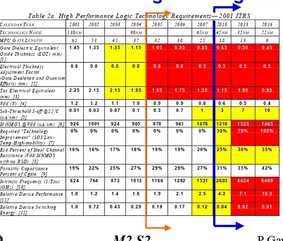
Table 2a High Performance Logic Technology Requirements— 2001 ITRS
C
ALEND AR
Y
EAR
2001
2002
2003
2004
2005
2006
2007
2010
2013
2016
T
ECH NO LO G Y
N
O D E
130
NM
90
NM
65
NM
45
NM
32
NM
22
NM
M PU G
ATE
L
ENG TH
65
53
45
37
32
30
25
18
13
9
Gate Dielectric Equivalent
Oxide Thickness (EOT) (nm)
[1]
1.45
1.35
1.35
1.15
1.05
0.95
0.85
0.65
0.50
0.45
Electrical Thickness
Adjustment Factor
(Gate Depletion and Quantum
Effects) (nm) [2]
0.8
0.8
0.8
0.8
0.8
0.8
0.5
0.5
0.5
0.5
Tox Electrical Equivalent
(nm) [3]
2.25
2.15
2.15
1.95
1.85
1.75
1.35
1.15
1.00
0.95
Vdd (V) [4]
1.2
1.2
1.1
1.0
0.9
0.9
0.8
0.6
0.5
0.4
Sub-Threshold I-off @25
°
C
(uA/ um) [5]
0.01
0.03
0.07
0.1
0.3
0.7
1
3
7
10
Id-NM OS @Vdd (uA/ um) [6]
926
1001
924
905
878
961
1076
1218
1523
1465
Required " Technology
Improvement" (SOI/
Low-Temp/ High-mobility) [7]
0%
0%
0%
0%
0%
0%
0%
30%
70%
100%
Rsd Percent of Ideal Channel
Resistance (Vdd/IdNM OS
with no RSD) [8]
16%
16%
17%
18%
19%
19%
20%
25%
30%
35%
Parasitic Capacitance
Percent of Cgate [9]
19%
22%
25%
27%
29%
29%
27%
31%
35%
42%
Intrinsic Frequency (1/Tau)
(GHz) [10]
624
764
873
1013
1166
1282
1531
2603
4424
6460
Relative Device Performance
[11]
1.0
1.2
1.4
1.6
1.9
2.1
2.5
4.2
7.1
10.3
Relative Device Switching
Energy [12]
M2 S2
P.Gargini
1.E-14
1.E-12
1.E-10
1.E-08
1.E-06
1.E-04
10
100
1000
Physical Gate Length (nm)
I
Off
(A/
µ
m)
Intel 15nm
transistor
Intel 30nm
transistor
Intel 20nm
transistor
Research data in literature ( )
Production data in literature ( )
1.E-06
1.E-05
1.E-04
1.E-03
1.E-02
1.E-01
1.E+00
1.E+01
1.E+02
1.E+03
5
10
15
20
25
Physical Tox (Å)
Jo
x
(A
/cm²) @1V In
v
e
rs
ion
SiO2 Gate Leakage
(from literature)
1.E-06
1.E-05
1.E-04
1.E-03
1.E-02
1.E-01
1.E+00
1.E+01
1.E+02
1.E+03
5
10
15
20
25
Physical Tox (Å)
Jo
x
(A
/cm²) @1V In
v
e
rs
ion
1.E-06
1.E-05
1.E-04
1.E-03
1.E-02
1.E-01
1.E+00
1.E+01
1.E+02
1.E+03
5
10
15
20
25
Physical Tox (Å)
Jo
x
(A
/cm²) @1V In
v
e
rs
ion
SiO2 Gate Leakage
(from literature)
M2 S2
P.Gargini
High
M2 S2
P.Gargini
Interconnect Grand Challenges
Near Term (2001-2007)
Enhancing Performance
■
Introduction of New Materials
:
●
High Conductivity and Low k Dielectric
■
Integration of New Processes and
Structures :
●
High Complexity
Long Term (2008-2016)
Enhancing Performance
■
Identify Solutions which address Global
Wiring Scaling:
●
Beyond Copper and Low k
●
Material Innovation to accelerate Design,
M2 S2
P.Gargini
®
®
Interconnect and
Interconnect and
Dielectric Materials
Dielectric Materials
1
2
3
R
e
si
st
iv
it
y
(
µµohm.cm)
2
3
1
Relative Dielectric Constant K
4
Cu
Air
Start
Aluminum
End
M2 S2
P.Gargini
Near Term (2001-2007)
Cost-effective Manufacturing
■
Coordinated Design Tools and
Simulators :
●
Mix Signal Co-design and Simulation
●
Transient Thermal Analysis Tool
●
Thermal Mechanical Analysis Tool
●
Electrical Analysis Tool
-
Power Disturbs
-
EMI
-
High Frequency / Current and
Lower Voltage Switching
Assembly & PKG Grand Challenges
Chip
Package
QFP
BGA
PGA
M2 S2
P.Gargini
M2 S2
P.Gargini
CMOS Future Directions
70%/2-3year
70% / 2-3year
Equivalent Scaling
2005-2014
??/2-3year
2X Performance/2-3year
Integrated Solutions
2000-2014
New Devices
2010-20XX
1970-2004
Traditional Scaling
Features
M2 S2
P.Gargini
The Ideal MOS Transistor
Fully Surrounding
Metal Electrode
High-K
Gate Insulator
Fully Enclosed,
Depleted
Semiconductor
Band Engineered
Semiconductor
Low Resistance
Source/Drain
Drain
Source
M2 S2
P.Gargini
Emerging Research Devices
Pursuing CMOS Scaling to the End
Bulk CMOS
–
Conventional bulk (SiO2, poly gate, etc..)
–
Introduction of new materials (high-K gate, metal gate
electrode,high mobility channel, etc.)
Non Classical CMOS Structures
–
Ultra thin channel (SOI)
–
Channel engineered structures
M2 S2
P.Gargini
BOXSource
Drain
Source
Gate
Drain
Si fin - Body!
FinFET
Band Engineered Transistor
Double Gate Transistor
Ultra-Thin Body SOI
2001 ITRS
New Transistor Definitions
M2 S2
P.Gargini
CNN
Nanotube
Molecular
SRT
SET
QD
RTD
M2 S2
Time
P.Gargini
Emerging Technology Sequence
SET
RSFQ
QCA
Molecular
RTD-FET
Strained
Si
Vertical
Transistor
FinFET
double gate
Planar
FD SOI
Quantum
computing
CNN
Defect
Tolerant
QCA
3D
Integration
Molecular
Architecture
Non-Classical
CMOS
Memory
Logic
Emerging
Technology
Vectors
Phase Change
Nano
SET
Molecular
Magnetic RAM
M2 S2
P.Gargini
Conclusions
•
The ITRS
has become a common
reference document
for the
Semiconductor Community
•
CMOS
will
remain
the device of choice for the foreseeable future
(>10yrs)
• Introduction of
Non-classical
CMOS in manufacturing will occur
within this decade
(~5years)
• Many
new materials
will be necessary->
Back to basics
• Design, Silicon Process, Package and System interaction will
continue to increase-> Need
integrated design
methodology
•
Innovation in:
Architecture, Logic, Memory and Devices is
marking the
Renaissance
of the Semiconductor Industry
•
Economical
challenges are
exceeding
the resources of any
individual company or consortium-> Cooperation is a must
M2 S2
P.Gargini
SUPPORT THE ITRS!!!!
SUPPORT THE ITRS!!!!
SUPPORT THE ITRS!!!!
SUPPORT THE ITRS!!!!