Sid Katzen
The Quintessential PIC
Microcontroller
SPIN Springer’s internal project number, if known
Engineering – Monograph (English)
November 8, 2000
Springer-Verlag
Berlin Heidelberg New York
London Paris Tokyo
Contents
List of Figures . . . . . VI
List of Tables . . . . . XI
List of Programs . . . . . XIV
Part I The Fundamentals
1. Digital Representation . . . . . 3
2. Logic Circuitry .. . . . 17
3. Stored Program Processing . . . . . 41
Part II The Software 4. The PIC16F84 Microcontroller .. . . . 77
5. The Instruction Set .. . . . 105
6. Subroutines and Modules .. . . . 137
7. Interrupt Handling . . . . . 171
8. Assembly language .. . . . 197
9. High-Level Language . . . . . 231
Part III The Outside World 10. The Real World . . . . . 253
VI Contents
12. One Bit at a Time . . . . . 305
13. Time is of the Essence .. . . . 361
14. Take the Rough with the Smooth . . . . . 391
15. To Have and to Hold . . . . . 431
16. A Case Study . . . . . 455
Appendices A. 14-bit Core Instruction Set .. . . . 475
B. Special Purpose Register Structure for the PIC16C74B .. . . . 477
C. CInstruction Set .. . . . 479
D. Acronyms and Abbreviations . . . . . 481
List of Figures
1.1 The NOT operation. . . 12
1.2 The AND function. . . 13
1.3 The inclusive-OR operation. . . 13
1.4 The XOR operation. . . 14
1.5 Detecting sign overflow. . . 15
2.1 The 74LS00 quad 2-I/P NAND package. . . 18
2.2 Output structures. . . 19
2.3 Open-collector buffers driving a party line. . . 20
2.4 Sharing a bus. . . 20
2.5 The 74LS138 and ’139 MSI natural decoders. . . 21
2.6 The 74LS688 octal equality detector. . . 23
2.7 Addition. . . 24
2.8 Implementing a programmable adder/subtractor. . . 25
2.9 The 74LS382 ALU. . . 25
2.10 A ROM-implemented 1-bit adder. . . 26
2.11 The 2764 Erasable PROM. . . 27
2.12 Floating-gate MOSFET link . . . 27
2.13 The R S latch. . . 29
2.14 Using a R S latch to debounce a switch. . . 30
2.15 The D latch and flip flop. . . 31
2.16 The 74LS74 dual D flip flop. . . 32
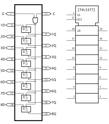
2.17 The 74LS377 octal D flip flop array. . . 33
2.18 The 74LS373 octal D latch array. . . 34
2.19 An 8-bit ALU-accumulator processor. . . 35
2.20 The SISO shift register. . . 36
2.21 The T flip flop. . . 36
2.22 A modulo-16 ripple counter. . . 37
2.23 Generating timing waveforms. . . 38
2.24 The 6264 8196×8 RAM. . . 39
3.1 An elementary von Neumann computer. . . 42
3.2 An elementary Harvard architecture computer. . . 44
3.3 Executing the 1st instruction whilst fetching down the 2nd. . . 45
VIII List of Figures
3.5 Programmer’s model. . . 54
3.6 The indirect mechanism. . . 57
3.7 Circular shifts. . . 61
3.8 The process. . . 65
3.9 Visualization of the taskprocess. . . 65
3.10 Division by repetitive subtracting. . . 68
3.11 Double-precision shifting. . . 70
3.12 A 7-bit pseudo-random number generator. . . 70
4.1 An example of a system based on a microcontroller. . . 81
4.2 Architecture of the PIC16F84 microcontroller . . . 85
4.3 Showing how all of the PCare altered when writing toPCL. . . . 86
4.4 Internal clocksequencing waveforms. . . 87
4.5 The PIC16F84 Status register . . . 89
4.6 Data store memory map. . . 92
5.1 General 14-bit core Status register. . . 109
5.2 The indirect mechanism. . . 109
5.3 The ith section of the compare-update sequence. . . 112
5.4 Generating a 13-bit Program-store address. . . 114
6.1 Modular hardware implementing a PC. . . 138
6.2 Subroutine calling. . . 140
6.3 Using the hardware stackhold return addresses. . . 141
6.4 Nested subroutines. . . 142
6.5 System view ofK×100 ms delay subroutine. . . 145
6.6 The 7-segment display. . . 148
6.7 System diagram for the byte multiplication subroutine. . . 150
6.8 The stackframe. . . 154
6.9 Finding the square root of an integer. . . 162
7.1 Detecting and measuring an external event. . . 172
7.2 Responding to an interrupt request. . . 175
7.3 The flag:maskpair. . . 176
7.4 The PIC 16F84’s interrupt logic. . . 178
7.5 Oven safety hardware. . . 188
7.6 Echo sounding hardware. . . 195
8.1 Conversion from assembly-level source to machine code. . . 198
8.2 Absolute assembly-level code translation. . . 202
8.3 Relocatable assembly-level code translation. . . 211
8.4 Linking three source files. . . 213
8.5 Code building and testing tools. . . 219
8.6 MPLAB window. . . 221
9.1 Conversion from high-level source code to machine code. . . 233
9.2 Onion skin view of the steps leading to executable code. . . 234
9.3 Simulating our example program in MPLAB. . . 242
9.4 The active-low die patterns. . . 250
10.1 Pinout for a variety of PIC family members. . . 254
10.2 Typical supply current versus clocking frequency. . . 256
10.3 Equivalent output circuit. . . 257
10.4 Typical oscillator configurations. . . 258
10.5 Configuration word for the PIC16F83/4. . . 261
10.6 Manually resetting the PIC. . . 263
10.7 The sequence of events leading to startup on power-up. . . 264
10.8 Brown-out reset. . . 267
10.9 An alternative brown-out circuit. . . 269
11.1 The mid-range PIC 16CXX series Parallel Ports A and B. . . 272
11.2 A simplified typical I/O port line. . . 273
11.3 Reading and writing to a port bit set to input or output. . . 275
11.4 Sinking and sourcing current. . . 276
11.5 Port A I/O pin driver structure. . . 278
11.6 Interfacing switches to a port line. . . 280
11.7 Port B’s weakpull-up option. . . 280
11.8 Interfacing to a keypad. . . 281
11.9 The Port B change feature. . . 285
11.10 A multi-zone intruder alarm. . . 287
11.11 Source current against voltage. . . 290
11.12 The stepper motor. . . 294
11.13 Using port expansion to drive three 7-segment displays. . . 298
11.14 Scanning a 3-digit 7-segment array. . . 299
11.15 Low-level output voltage against sinkcurrent. . . 304
12.1 The smart card. . . 305
12.2 Serial interface to a 3-digit 7-segment display. . . 307
12.3 Logic functional diagram of the 74HCT595 octal shift register. 309 12.4 Serially interfacing to a DAC0800 digital to analog converter. 310 12.5 Serially interfacing to the multi-zone intruder alarm. . . 311
12.6 The MAX549A SPI dual 8-bit DAC. . . 314
12.7 SPI waveforms for the MAX549A. . . 316
12.8 Multiple MAX549As on the one SPI circuit. . . 316
12.9 The basic Serial Synchronous Port. . . 317
12.10 The SSP CONtrol and STATus registers. . . 318
12.11 SSP SPI-mode master waveforms. . . 321
12.12 A multidrop SPI communications network. . . 322
12.13 Data transfer on theI2Cbus. . . 325
X List of Figures
12.15 AI2Cpacket transmission. . . 327
12.16 The MAXIM MAX518I2Cdual digital to analog converter. . . 328
12.17 Minimum timing relationships for the FastI2Cmode. . . 329
12.18 Transmitting the string "PIC" in the asynchronous mode . . . 336
12.19 The PIC USART configured for asynchronous communication. 342 12.20 Some signalling configurations. . . 347
12.21 Communicating with a PC via an RS-232 link. . . 349
12.22 The 24XXX series of I2C serial EEPROMs. . . 352
12.23 EEPROM Read and Write waveforms. . . 355
12.24 Interfacing the DS1820 1-Wire digital thermometer. . . 356
12.25 A LCD display. . . 360
13.1 The integral PIC Watchdog timer. . . 362
13.2 The Option register. . . 363
13.3 Simplified equivalent circuit for Timer 0. . . 365
13.4 Counting cans of beans on a conveyer belt. . . 366
13.5 Functional equivalent circuit for Timer 1 . . . 372
13.6 The CCP1 module set to Compare mode. . . 375
13.7 Capturing the time of an event. . . 377
13.8 A simplified equivalent circuit for Timer 2. . . 379
13.9 Pulse width modulation. . . 380
13.10 Timer 2 and the PWM CCP mode. . . 381
13.11 An event manifesting itself as a pulse duration. . . 387
14.1 Analog world – digital processing. . . 391
14.2 The quantizing process. . . 393
14.3 The analog–digital process. . . 396
14.4 Illustrating aliasing. . . 397
14.5 Initializing the 8-4-2-1 capacitor network. . . 398
14.6 Simplified view of the A/D converter. . . 400
14.7 The successive approximation process. . . 402
14.8 The 8-bit 8-channel analog to digital conversion module. . . 404
14.9 Configuring the analog inputs for Port A and Port E. . . 405
14.10 Interrupt control for the ADC module. . . 408
14.11 R-2R digital-to-analog conversion. . . 416
14.12 The Maxim MAX506 quad 8-bit D/A converter. . . 418
14.13 Generating a continuous sawtooth using a MAX506 DAC. . . 419
14.14 Buffered data acquisition. . . 420
14.15 A level-shifting resistor network. . . 423
14.16 ECG detection strategy. . . 426
14.17 A controllable external voltage circuit. . . 429
14.18 Pinning for the PIC16C71. . . 429
15.1 The PIC16F8X Data EEPROM module. . . 433
15.3 The first 32 bytes of EEPROM. . . 438
15.4 The PIC16F87X flash and Data EEPROM storage system. . . 440
15.5 The PIC16F87X EEPROM Control register 1. . . 441
15.6 View of the flash Program module. . . 445
15.7 Configuration word for the PIC16F87X devices. . . 445
15.8 Watchdog timer period versus temperature. . . 448
16.1 The annunciator hardware. . . 456
16.2 The modular software structure. . . 458
16.3 The Main process. . . 468
16.4 Programming the PIC from MPLAB. . . 472
List of Tables
1.1 7-bit ASCII characters. . . 5
1.2 Some common bit groupings. . . 6
1.3 Different ways of representing the quantities decimal 0…20. . 7
3.1 Our BASIC computer’s instruction set. . . 53
5.1 Move instructions. . . 115
5.2 Arithmetic. . . 117
5.3 Logic instructions. . . 121
5.4 Program Counter instructions. . . 127
6.1 Subroutine and interrupt handling instructions. . . 139
6.2 The 7-segment lookup table showing byte[N] being extracted. 149 8.1 The listing fileroot.lst. . . 206
8.2 The absolute 8-bit Intel format object-code fileroot.hex. . . . 206
8.3 The error file . . . 207
8.4 Part of Microchip’s file p16f84.inc. . . 209
8.5 Thepic16f84.lkr linker command file. . . 212
8.6 The output linker map filerms.asm. . . 218
8.7 The resulting absolute object file rms.hex. . . 219
9.1 Resulting assembly-level CCS compiler output after linking. . . 240
10.1 PIC16F83/4 Special-Purpose Register file reset summary. . . 263
10.2 Power-up reset andsleeptimeouts. . . 265
10.3 Reset conditions. . . 266
11.1 Summary of mid-range PIC parallel I/O provision. . . 272
11.2 Energization pattern for the eight field directions. . . 294
12.1 The SSP Mode bits. . . 319
14.1 Quantization parameters. . . 394
14.2 ADC clocking frequency versus device crystal frequency. . . 401
List of Programs
3.1 Clearing a blockof files the linear way. . . 56
3.2 Clearing a blockof files using a repeating loop. . . 57
3.3 Simple single-precision addition of two byte variables. . . 64
3.4 A more accurate single-precision addition. . . 64
3.5 The double-precision add program. . . 66
3.6 Dividing by ten. . . 67
3.7 Multiplying by nine. . . 69
3.8 A 7-bit pseudo-random number generator. . . 71
4.1 Incrementing a packed BCD byte. . . 101
4.2 Adding two packed BCD numbers. . . 103
5.1 Finding the maximum temperature the linear way. . . 111
5.2 Finding the maximum temperature using a loop structure. . . . 113
5.3 Division by repetitive subtraction. . . 118
5.4 Shifting to find the highest set bit. . . 124
5.5 Triple-precision shifting to find the number of set bits. . . 125
5.6 Multiplying by three. . . 126
5.7 Double-precision decrement. . . 128
5.8 Bi-quinary error detection. . . 130
5.9 Binary to 2-digit BCD conversion. . . 131
5.10 Average daily temperature. . . 132
5.11 multiplication by ten. . . 133
6.1 A 100 ms delay subroutine. . . 144
6.2 AK×100 ms delay subroutine. . . 146
6.3 An alternativeK×100 ms delay subroutine. . . 147
6.4 The software 7-segment decoder. . . 149
6.5 The byte multiplication subroutine. . . 152
6.6 Implementing a byte multiply using a stackmodel. . . 157
6.7 Dividing by three . . . 158
6.8 Coding a 208µs delay. . . 159
6.9 A 1-second delay program. . . 160
6.10 Binary to 3-digit BCD conversion. . . 161
6.11 Coding the square root subroutine. . . 163
6.12 Using a software stackto pass parameters. . . 166
XVI List of Programs
7.1 Background program for the pea canning packer. . . 181
7.2 Event counting foreground software. . . 183
7.3 Oven safety. . . 187
7.4 Saving and restoring the context for the PIC16C74 processor. 191 7.5 Coding the real-time clockISR. . . 193
7.6 Incrementing a packed-BCD byte with maximum value of 99. . 194
8.1 Absolute assembly-level code for our square-root module. . . . 200
8.2 The main relocatable source file main.asm. . . 214
8.3 The relocatable source filesqr.asm. . . 215
8.4 The relocatable source fileroot2.asm. . . 216
9.1 A simple function coded inC. . . 236
9.2 Coding the square root function. . . 245
9.3 Linearizing a K-type thermocouple. . . 246
9.4 Generating the root-mean square value of two variables. . . 247
11.1 Scanning the keypad. . . 283
11.2 Noise filtered keypad scanning. . . 284
11.3 Interacting with the intruder hardware. . . 288
11.4 A digital comparator with hysteresis. . . 292
11.5 Driving a stepper motor. . . 293
11.6 Coding the keypad device driver inC. . . 297
11.7 Displaying the decimal equivalent of a binary byte. . . 301
11.8 Displaying a 3-digit decimal number on a scanning readout. . 302
12.1 Displaying the decimal equivalent of a binary byte. . . 308
12.2 Input serial byte subroutine. . . 312
12.3 Interacting with the MAX549A dual-channel SPI DAC. . . 315
12.4 Using the SSP for SPI data input and output. . . 320
12.5 Interfacing to the MAX549A inC. . . 323
12.6 A crystal frequency-independent short delay macro. . . 331
12.7 Low-levelI2Csubroutines. . . 332
12.8 Interacting with the MAX518 dual-channel I2C DAC. . . 334
12.9 Interfacing to the MAX518 inC. . . 335
12.10 A baud-rate delay macro. . . 338
12.11 Asynchronous formatted input and output subroutines. . . 340
12.12 The USART-based I/O subroutines. . . 345
12.13 Updating Program 11.4’s trip value. . . 350
12.14 Reading in a byte using theI2Cprotocol. . . 351
12.15 Incrementing the non-volatile odometer count. . . 354
12.16 Reading and writing on a 1-Wire system. . . 358
13.1 The bean counter Interrupt Service Routine. . . 368
13.2 Measuring the ECG waveform period to a resolution of 1 ms. . 370
13.3 Generating a 15 minute data logger timebase. . . 374
13.4 Capturing the instant of time an ECG R-point occurs. . . 378
13.5 Pulse-Width Modulation using Timer 0. . . 384
13.7 Measuring the duration of a pulse. . . 388
14.1 Taking a reading from channeln. . . 407
14.2 Interrupt-driven subroutine to read channeln. . . 410
14.3 The ISR for our interrupt-driven ADC software. . . 411
14.4 Digitizing Channel 1 of a PIC16C71 device. . . 412
14.5 A digital/analog comparator with hysteresis. . . 414
14.6 Buffered interrupt-driven data acquisition. . . 421
14.7 Sleep conversion in C. . . 422
14.8 ECG peakpicking. . . 425
14.9 An implementation of the ECG peakpicker inC. . . 427
15.1 Retrieving a byte from the EEPROM Data module. . . 434
15.2 Putting a byte into the EEPROM Data module. . . 436
15.3 Incrementing the non-volatile odometer count in Data EEPROM. 437 15.4 Reading a word from the flash Program store. . . 442
15.5 Writing to flash Program memory. . . 443
15.6 Squaring an integer. . . 444
15.7 C-based coding for the odometer. . . 446
15.8 The Sauna Power-up reset sequence and ISR. . . 450
15.9 Reading a new period count. . . 451
15.10 Updating the Sauna EEPROM. . . 452
16.1 The timebase software. . . 461
16.2 The data display function. . . 463
16.3 The initialization code. . . 465
16.4 The Diagnostic process. . . 466
16.5 The Set-time process. . . 467
PART I
The Fundamentals
This bookis about microcontrollers (MCUs). These are digital engines modelled after the architecture of a stored-program computer and in-tegrated on to a single very large-scale inin-tegrated circuit together with support circuitry, memories and peripheral interface devices. Although the MCU is often confused with its better known cousin the micropro-cessor in its role of the driving force of the ubiquitous personal com-puter, the vast majority of both microprocessors and microcontrollers are embedded into an assemblage of other digital components. The first microprocessors in the early 1970s were marketed as an alternative way of implementing digital circuitry. Here the taskwould be determined by a series of instructions encoded as binary code groups in read-only memory. This is more flexible than the alternative approach of wiring hardware integrated circuits in the appropriate manner. The microcon-troller is simply the embodiment of this original role of the integrated computer.
We will lookat embedded MCUs in a general digital processing context in Parts II and III. Here our objective is to lay the foundation for this material. We will be covering:
• Digital code patterns.
• Binary arithmetic.
• Digital circuitry.
• Computer architecture and programming.
This will by no means be a comprehensive review of the subject, but there are many other excellent texts in this area1 which will launch you into greater depths.
CHAPTER 1
Digital Representation
To a computer or microprocessor, the world is seen in terms of patterns of digits. Thedecimal (or denary) system represents quantities in terms of the ten digits 0…9. Together with the judicious use of the symbols +,− and . any quantity in the range±∞can be depicted. Indeed non-numeric concepts can be encoded using numeric digits. For example the American Standard Code for Information Interchange (ASCII) defines the alphabetic (alpha) characters A as 65, B = 66…Z = 90 and a = 97, b = 98…z = 122 etc. Thus the string “Microprocessor” could be encoded as “77, 105, 99, 114, 111, 112, 114, 111, 99, 101, 115, 115, 111, 114”. Provided you know the context, that is what is a pure quantity and what is text, then just about any symbol can be coded as numeric digits.1
Electronic circuits are not very good at storing and processing a mul-titude of different symbols. It is true that the first American digital com-puter, the ENIAC (Electronic Numerical Integrator And Calculator) in 1946 did its arithmetic in decimal2 but all computers since handle data in bi-nary(base 2) form. The decimal (base 10) system is really only convenient for humans, in that we have ten fingers.3 Thus in this chapter we will look at the properties of binary digits, their groupings and processing. After reading it you will:
• Understand why a binary data representation is the preferred base for digital circuitry.
• Know how a quantity can be depicted in natural binary, hexadecimal and binary coded decimal.
• Be able to apply the rules of addition and subtraction for natural binary quantities.
• Know how to multiply by shifting left.
• Know how to divide by shifting right and propagating the sign bit.
• Understand the Boolean operations of NOT, AND, OR and XOR.
The information technology revolution is based on the manipulation, computation and transmission of digitized information. This
informa-1Of course there are lots of encoding standards, for example the 6-dot Braille code for
the visually impaired.
tion is virtually universally represented as aggregrates of binary digits (bits).4 Most of this processing is effected using microprocessors, and it is sobering to reflect that there is more computing power in a singing birthday card than existed on the entire planet in 1950!
Binary is the universal choice for data representation, as an electronic switch is just about the easiest device that can be implemented using a transistor. Such 2-state switches are very small; they change state very quickly and consume little power. Furthermore, as there are only two states to distinguish between, a binary depiction is likely to be resistant to the effects of noise. The upshot of this is that both the packing density on a silicon chip and switching rate can be very high. Although a switch on its own does not represent much computing power; five million switches changing at 100 million times a second, manage to present at least a facade of intelligence!
The two states of a bit are conventionally designated logic 0 and
logic 1 or just 0 & 1. A bit may be represented by two states of any number of physical quantities; for example electric current or voltage, light, pneumatic pressure. Most microprocessors use 0 V (or ground) for state 0and 3 – 5 V for state1, but this is not universal. For instance, the RS232 serial port on your computer uses nominally +12 V for state0and
−12 V for state1.
A single bit on its own can only represent two states. By dealing with groups of bits, rather more complex entities can be coded. For example the standard alphanumeric characters can be coded using 7-bit groups of digits. Thus the ASCII code for “Microprocessor” becomes:
1001101 1101001 1100011 1110010 1101111 1110000 1110010 1101111 1100011 1100100 1110011 1110011 1101111 1110010
Unicode is an extension of ASCII and with its 16-bit code groups is able represent characters from many languages and mathematical symbols.
The ASCII code isunweighted, as the individual bits do not signify a particular quantity; only the overall pattern has any significance. Other examples are the die code on gaming dice and 7-segment code of Fig. 6.6 on page 148. Here we will deal with natural binary weighted codes, where the position of a bit within the number field determines its value or weight. In an integer binary number the rightmost digit is worth 20 =1, the next left column 21=2 and so on to thenth column which is worth 2n−1. For example the decimal number one thousand nine hundred and ninety eight is represented as 1×10³+9×10²+9×101+8×100or 1998.
4The binary base is not a new fangled idea invented for digital computer; many cultures
1. Digital Representation 5
Table 1.1: 7-bit ASCII characters.
NUL SOH STX ETX EOT ENQ ACK BEL BS HT LF VT FF CR SO SI EM US RS GS ESC FS SUB SYN NAK DC1 DC2 CAN ETB DC4 DC3 DLE ) / . -+ , * & % ! " ( ’ $ # SP 9 ? > = ; < : 6 5 1 2 8 7 4 3 0 I O N M K L J F E A B H G D C @ Y } [ \ Z V U Q R X W T S P i o n m k l j f e a b h g d c ‘ y DEL ~ } { | z v u q r x w t s p LS nybble MS nybble ^
_
Innatural binarythe same quantity is 1×210+1×29+1×28+1×27+ 1×26+0×25+0×24+1×23+1×22+0×21+1×20, or11111001101b. Fractional numbers may equally well be represented by columns to the right of the binary point using negative powers of 2. Thus 1101.11b is equivalent to 14.75. As can be seen from this example, binary numbers are rather longer than their decimal equivalent; on average a little over three times. Nevertheless, 2-way switches are considerably simpler than 10-way devices, so the binary representation is preferable.
micropro-cessor, the Intel 4004, handled its data four bits (a nybble) at a time. Many current processors cope with blocks of 8 bits (a byte), 16 bits (a
word), or 32 bits (a long-word). 64-bit (aquad-word) devices are on the horizon. These groupings are shown in Table 1.2. The names illustrated are somewhat de-facto, and variations are sometimes encountered.
As in the decimal number system, large binary numbers are often expressed using the prefixes k (kilo), M (mega) and G (giga). A binary kilo is 210 = 1024; for example 64 kbyte of memory. In an analogous way, a binary mega is 220 =1,048,576; thus a 1.44 Mbyte floppy disk. Similarly a 2 Gbyte hard diskhas a storage capacity of 2×230 = 2,147,483,648 bytes. The former representation is certainly preferable.
Table 1.2: Some common bit groupings.
(0000 0000 0000 0000 0000 0000 0000 0000−1111 1111 1111 1111 1111 1111 1111 1111)
(32 bits) 0−4,294,967,295 (1 bit) 0−1
(0−1)
(4 bits) 0−15
(0000−1111)
(8 bits) 0−255
(0000 0000−11111 1111)
(16 bits) 0−65,535
(0000 0000 0000 0000−1111 1111 1111 1111) Bit
Nybble
Byte
Word
Long-word
Long binary numbers are not very human friendly. In Table 1.2, bi-nary numbers were zoned into fields of four digits to improve readability. Thus the address of a data unit stored in memory might be 1000 1100 0001 0100 0000 1010b. If each group of four can be given its own symbol, 0…9 and A…F, as shown in Table 1.3, then the address becomes 8C140Ah; a rather more manageable characterization. This code is called
hexadecimal, as there are 16 symbols. Hexadecimal (base-16) numbers are a viable number base in their own right, rather than just being a con-venient binary representation. Each column is worth 160,161,162. . .16n in the normal way.5
Binary Coded Decimal is a hybrid binary/decimal code extensively used at the input/output ports of a digital system (see Example 11.5 on page 298). Here each decimal digit is individually replaced by its 4-bit binary equivalent. Thus 1998 is coded as (0001 1001 1001 1000)BCD. This is very different from the equivalent natural binary code; even if it is represented by 0s and 1s. As might be expected, arithmetic in such
5Many scientific calculators, including that in the Accessories group under Windows 95,
1. Digital Representation 7
Table 1.3: Different ways of representing the quantities decimal 0…20.
Decimal Natural binary Hexadecimal Binary
00 00000 00 0000 0000
01 00001 01 0000 0001
02 00010 02 0000 0010
03 00011 03 0000 0011
04 00100 04 0000 0100
05 00101 05 0000 0101
06 00110 06 0000 0110
07 00111 07 0000 0111
08 01000 08 0000 1000
09 01001 09 0000 1001
10 01010 0A 0001 0000
11 01011 0B 0001 0001
12 01100 0C 0001 0010
13 01101 0D 0001 0011
14 01110 0E 0001 0100
15 01111 0F 0001 0101
16 10000 10 0001 0110
17 10001 11 0001 0111
18 10010 12 0001 1000
19 10011 13 0001 1001
20 10100 14 0010 0000
a hybrid system is difficult, and BCD is normally converted to natural binary at the system input and processing is done in natural binary before being converted back(see Program 5.9 on page 131).
The rules of arithmetic are the same in natural binary6 as they are in the more familiar base 10 system, indeed any base-n radix scheme. The simplest of these is addition, which is a shorthand way of totalling quantities, as compared to the more primitive counting or incrementa-tion process. Thus 2+4= 6 is rather more efficient than 2+1 =3; 3+1 = 4; 4+1 = 5; 5+1 = 6. However, it does involve memorizing the rules of addition.7 In decimal this involves 45 rules, assuming that order is irrelevant; from 0+0= 0 to 9+9=18. Binary addition is much simpler as it is covered by only three rules:
0+0 = 0
0+1 1+0
= 1
1+1 =10 (0carry 1)
Based on these rules, the least significant bit (LSB) is totalized first, pass-ing a carryif necessary to the next left column. The process ends with
the most significant bit (MSB) column, its carry being the new MSD of the sum. For example:
96 Augend + 37 Addend
133 Sum
1 Carries
1100000 Augend + 0100101 Addend
10000101 Sum
1 1
1 Carries
0 1 42684 21
1 3 6 1
(a) Decimal (b) Binary
8 2 1 0
1
0
Just as addition implements an up count,subtractioncorresponds to a down count, where units are removed from the total. Thus 8−5 =3 is the equivalent of 8−1=7; 7−1=6; 6−1=5; 5−1=4; 4−1=3.
The technique of decimal subtraction you are familiar with applies the subtraction rules commencing from LSB and working to the MSB. In any given column were a larger quantity is to be taken away from a smaller quantity, a unit digit isborrowedfrom the next higher column and given backafter the subtraction is completed. Based on this borrow principle, the subtraction rules are given by:
0 − 0 = 0 10
− 1 = 1 Borrowing1from the higher column 1 − 0 = 1
1 − 1 = 0
For example:
96 Minuend - 37 Subrahend
59 Difference
1 Borrows
1100000 Minuend - 0100101 Subrahend
0111011 Difference
1
1 Borrows
0 1 42684 21
1 3 6 1
(a) Decimal (b) Binary
1 1 1 1
Although this familiar method works well, there are several problems implementing it in digital circuitry.
• How can we deal with situations where the minuend is larger than the subtrahend?
• How can we distinguish between positive and negative quantities?
• Can a digital system’s adder circuits be coerced into subtracting?
1. Digital Representation 9
37 Minuend - 96 Subtrahend
41 Difference (- 59)
1
0100111 Minuend - 1100000 Subtrahend
1000111 Difference (- 0111001)
1
(a) Decimal (b) Binary
Normally when we know that the when Minuend is greater than the Subtrahend, the two operands are interchanged and a minus sign is ap-pended to the outcome; that is −(Subtrahend−Minuend). If we do not swap, as in (a) above, then the outcome appears to be incorrect. In fact 41 is correct, in that this is the difference between 59 (the correct outcome) and 100. 41 is described as the 10’s complement of 59. Furthermore, the fact that a borrow digit was generated from the MSD indicates that the difference is negative, and therefore appears in this 10’s complement form. Converting from 10’s complement decimal numbers to the ‘nor-mal’ magnitude form is simply a matter of inverting each digit and then adding one to the outcome. A decimal digit is inverted by computing its difference from 9. Thus the 10’s complement of 3941 is−6059:
3941 ⇒6058;+1= −6059
However, there is no reason why negative numbers should not remain in this complement form – just because we are not familiar with this type of notation.
The complement method of negative quantity representation of course applies to binary numbers. Here the ease of inversion (0→1;1→0) makes this technique particularly attractive. Thus in our example above:
1000111 ⇒0111000;+1= −0111001
Again, negative numbers should remain in a2’s complementform. This complement process is reversible. Thus:
complement⇐⇒normal
Signed decimal numeration has the luxury of using the symbols + and − to denote positive and negative quantities. A 2-state system is stuckwith 1s and 0s. However, looking at the last example gives us a clue on how to proceed. A negative outcome gives a borrow backout to the highest column. Thus we can use this MSD as a sign bit, with 0for
+ and 1 for −. This gives 1,1000111b for −59 and 0,01110011b for
0,1100000 (+96) 1,1011011 (- 37)
0,0111011 (+59)
1
0,0100101 (+37) 1,0100000 (- 96)
1,1000101 (- 59)
(a) Minuend less than subtrahend (b) Minuend greater than subtrahend
1
From this example we see that if negative numbers are in a signed 2’s complement form, then we no longer have the requirement to implement hardware subtractors, as adding a negative number is equivalent to sub-tracting a positive number. Thus A−B= A+(−B). Furthermore, once numbers are in this form, the outcome of any subsequent processing will always remain 2’s complement signed throughout.
There are two difficulties associated with signed 2’s complement arith-metic. The first of these isoverflow. It is possible that adding two pos-itive or two negative numbers will cause overflow into the sign bit; for instance:
(a) Sum of two +ve numbers gives - ve (b) Sum of two - ve numbers gives +ve 1,0011 (- 13!!!)
0,1011 (+11) 0,1000 (+8)
0,1101 (+3!!!) 1,0101 (- 11) 1,1000 (- 8)
1 1
In (a) the outcome of (+8)+(+11) is −13! The 24 numerical digit has overflowed into the sign position (actually, 10011b = 19 is the correct outcome). Example (b) shows a similar problem for the addition of two signed negative numbers. Overflow can only happen if both operands have the same sign bits. Detection is then a matter of determining this situation with an outcome that differs. See Fig. 1.5 for a logic circuit to implement this overflow condition.
The final problem concerns arithmetic on signed operands with dif-ferent sized fields. For instance:
0,0011001 (+25) 0,011 (+03)
???? 1
0,0011001 (+25) 1,101 (- 03)
????
(a) Extending a positive number (b) Extending a negative number
0,0011100 (+28) 0,0011001 (+25) 0,0000011 (+03)
0,0011001 (+25)
0,0010110 (+22) 1
1 1 1 1 1
1. Digital Representation 11
Both the examples involve adding an 8-bit to a 16-bit operand. Where the former is positive, the data may be increased to 16 bits by padding with 0s. The situation is slightly less intuitive where negative data re-quires extension. Here the prescription is to extend the data by padding out with 1s. In the general case the rule is simply to pad out data by propagating the sign bit left. This technique is known assign extension. Multiplication by thenth power of two is simply implemented by shift-ing the data leftnplaces. Thus00101(5) <<01010(10) <<10100(20)
multiplies 5 by 22, where the<<operator is used to denote shifting left. The process works for signed numbers as well:
0,00000011 ( 3) <<
0,00000110 ( 6) <<
0,00001100 (12) <<
0,00011000 (24)
(a) +3 x 8 = +24 (b) - 3 x 8 = - 24
1,11110100 (- 12)
1,11101000 (- 24) 1,11111010 ( - 6) 1,11111101 ( ¡3)
<< << <<
0,00000110 (3 x 2) + 0,00011000 (3 x 8)
0,00011110 (3 x 10 = 30)
(c) +3 x 10 = 30
Should the sign bit change polarity, then a magnitude bit has overflowed. Some computers/microprocessors have a Arithmetic Shift Left process that signals this situation, as opposed to the standard Logic Shift Left used in unsigned number shifts.
Multiplication by non-powers of 2 can be implemented by a combi-nation of shifting and adding. Thus as shown in (c) above, 3 × 10 is implemented as(3×8)+(3×2)=(3×10)or(3<<3)+(3 <<1).
In a similar fashion, division by powers of 2 is implemented by shifting rightnplaces. Thus1100(12) >>0110(6) >>0011(3) >>0001.1(1.5). This process also works for signed numbers:
>>
>>
>>
(a) +15/8 = 1.875 (b) - 15/8 = - 1.875
>> >> >>
(c) 15/10 = 1.5
1010 1111.0 0001.1 - 1010 0101 - 101.0 000.0 1,11110.001 (- 1.875)
1,1100.010 (- 3.75) 1,1000.100 (- 7.5) 1,0001.000 (- 15) 0,1111.000 (+15)
0,0111.100 (+7.5)
0,0011.110 (+3.75)
0,0001.111 (+1.875)
Notice that rather than always shifting in0s, the sign bit should be prop-agated in from the left. Thus positive numbers shift in 0s and negative numbers shift in1s. This is known asArithmetic Shift Rightas opposed toLogic Shift Rightwhich always shifts in0s.
analagous process to the shift and add technique for multiplication, using a combination of shifting and subtracting.
Arithmetic is not the only way to manipulate binary patterns. George Boole8 in the mid-19th century developed an algebra dealing with sym-bolic processing of logic propositions. This Boolean algebra deals with variables which can be true or false. In the 1930s it was realised that this mathematical system could equally well be used to analyze switching net-works and thus binary logic systems. Here we will confine ourselves to looking at the fundamental logic operations of this switching algebra.
A f
0 1 1 0
A f = A
1
A f = A
(a) Truth table (b) Alternative logic symbols
Fig. 1.1 The NOT operation.
The inversion orNOT operation is represented by overscoring. Thus f = A states that the variable f is the inverse of A; that is if A= 0 then f = 1 and if A=1 then f = 0. In Fig. 1.1(a) this transfer characteristic is presented in the form of a truth table. By definition, inverting twice returns a variable to its original state; thusf = f.9
Logic function implementations are normally represented in an ab-stract manner rather than as a detailed circuit diagram. TheNOT gateis symbolized as shown in Fig. 1.1(b). The circle always represents inver-sion in a logic diagram, and is often used in conjunction with other logic elements, such as in Fig. 1.2(c).
TheAND operatorgives anall or nothing function. The outcome will only be true wheneveryone of theninputs are true. In Fig. 1.2 two input variables are shown, and the output is symbolized as f = B·A, where · is the Boolean AND operator. The number of inputs is not limited to two, and in generalf =A(0)·A(1)·A(2)· · ·A(n). The AND operator is
8The first professor of mathematics at Queen’s College, Cork.
9In days of yore when logic circuits were built out of discrete devices, such as diodes,
1. Digital Representation 13
B A f
0 0 0 0 1 0
A
f = B A
&
A
f = B A
(a) Truth table (b) Alternative logic symbols
1 1 1
1 0 0 B
B
(c) NAND
1 1 0 0 0 1 0 1 1 1 0 1 B A f
B f = B A
A B A
&
f = B A
Fig. 1.2 The AND function.
sometimes called a logic product, as ANDing (cf. multiplying) any bit with logic0always yields a 0output.
If we consider B as a control input and A as a stream of data, then consideration of the truth table shows that the output follows the data stream when B=1and is always 0when B=0. Thus the circuit can be considered to be acting as a valve, gating the data through on command. The term gate is generally applied to any logic circuit implementing a fundamental Boolean operator.
Most practical AND gate implementations have an inverting output. The logic of such implementations is NOT AND, or NAND for short, and is symbolized as shown in Fig. 1.2(c).
B A f
0 0 0 0 1 1
A
f = B + A
>1
A
f = B + A
(a) Truth table (b) Alternative logic symbols
1 1 1
1 0 1 B
B
(c) NOR
1 1 0 0 0 1 0 1 0 1 0 0 B A f
B f = B + A
A B A
>1
f = B + A
Fig. 1.3 The inclusive-OR operation.
Considering B as a control input and A as data (or vice versa), then from Fig. 1.3(a) we see that the data is gated through when B is 0 and inhibited (always 1) when B is 1. This is a little like the inverse of the AND function. In fact the OR function can be expressed in terms of AND using the duality relationship A+B= B·A. This states that the NOR function can be implemented by inverting all inputs into an AND gate.
AND, OR and NOT are the three fundamental Boolean operators. There is one more operation commonly available as an electronic gate; the
Exclusive-OR operator(XOR). The XOR function is true ifonly oneinput is true (hence the=1label in the logic symbol). Unlike the inclusive-OR, the situation where both inputs are true gives a false outcome.
B A f
0 0 0 0 1 1
A
f = B + A
=1
A
f = B + A
(a) Truth table (b) Alternative logic symbols
1 1 0
1 0 1 B
B
(c) ENOR
B f = B + A
A B A
=1
f = B + A
1 0 0
1 1 1
0 1 0
0 0 1 B A f
Fig. 1.4 The XOR operation.
If we considerBis a control input and A as data (they are fully inter-changeable) then:
• WhenB=0then f =A; that is the output follows the data input.
• When B=1 then f =A; that is the output is the inverse of the data input.
Thus an XOR gate can be used as a programmable inverter.
Another useful property considers the XOR function as a logic differ-entiator. The XOR truth table shows that the gate gives a true output if the two inputs differ. Alternatively, the ENOR truth table of Fig. 1.4(c) shows a true output when the two inputs are the same. Thus an ENOR gate can be considered to be a 1-bit equality detector. The equality of two
n-bit words can be tested by ANDing an array of ENOR gates (see Fig. 2.6 on page 23), each generating the functionBk⊕Ak; that is:
fB=A = n−1
k=0
Bk ⊕Ak
1. Digital Representation 15
bit of the outcome word C is not the same as either of these sign bits, say SB⊕SC. The logic diagram for this detector is shown in Fig. 1.5 and implements the Boolean function:
(SB⊕SA)·(SB⊕SC)
SA B S
C S
S = SA B
S = SC B
V
is true if:
(Sign A = Sign B) AND (Sign C = Sign B) V
Fig. 1.5 Detecting sign overflow.
CHAPTER 2
Logic Circuitry
We have noted that digital processing is all about transmission, manip-ulation and storage of binary word patterns. Here we will extend the concepts introduced in the last chapter as a lead into the architecture of the computer and microprocessor. We will lookat some relevant logic functions, their commercial implementations and some practical consid-erations.
After reading this chapter you will:
• Understand the properties and use of active pull-up, open-collector and 3-state output structures.
• Appreciate the logic structure and function of the natural decoder.
• See how a MSI implementation of an array of ENOR gates can compare two words for equality.
• Understand how a 1-bit adder can be constructed from gates, and can be extended to deal with the addition of twon-bit words.
• Appreciate how the function of an ALU is so important to a pro-grammable system.
• Be aware of the structure and utility of a read-only memory (ROM).
• Understand how two cross-coupled gates can implement a R S latch.
• Appreciate the difference between a D latch and D flip flop.
• Understand how an array of D flip flops or latches can implement a register.
• See how a serial connection of D flip flops can perform a shifting func-tion.
• Understand how a D flip flop can act as a frequency divide by two, and how a cascade of these can implement a binary count.
• See how an ALU/PIPO register can implement an accumulator processor unit.
• Appreciate the function of a RAM.
1 2 3 4 5 6 7 8 9 10 11 12 13 14 Vcc GND 1A 1B 1Y 2A 2B 2Y 4B 4A 4Y 3B 3A 3Y [74LS00] & 1A 1B 1Y (1) (2) (3) 2B 2A (5) (4) (6) 2Y 3B 3A (10) (9) (8) 3Y 4B 4A (13) (12) (11) 4Y
(a) DIL package (b) ANSI/IEC logic symbol
Fig. 2.1 The 74LS00 quad 2-I/P NAND package.
The 74LS001comprises four 2-input NAND gates in a 14-pin package. The integrated circuit (IC) is powered with a 5±0.25 V supply between VCC2 (usually about 5 V) andGND.The logic outputs are 2.4 – 5 V High and 0 – 0.4 V for Low. Most IC logic families require a 5 V supply, but 3 V versions are becoming available, and some CMOS implementations can operate with a range of supplies between 3 V and 15 V.
The 74LS00 IC is shown in Fig. 2.1(a) in its Dual In-Line (DIL) pack-age. Strictly it should be described as a positive-logic quad 2-I/P NAND, as the electrical equivalent for the two logic levels 0 and 1 are Low (L is around ground potential) and High (H is around Vcc,3 usually about 5 V). If the relationship 0→H; 1→L is used (negative logic) then the 74LS00 is actually a quad 2-I/P NOR gate. The ANSI/IEC4 logic symbol of Fig. 2.1(b) denotes a Low electrical potential by using the polarity symbol. The ANSI/IEC NAND symbol shown is thus based on the real electrical operation of the circuit. In this case the logic coincides with a
1The LS stands for “Low-power Schottky transistor”. There are very many other
ver-sions, such as ALS (Advanced LS), AS (Advanced Schottky) and HC (High-speed Com-plementary metal-oxide transistor – CMOS). These family variants differ in speed and power consumption, but for a given number designation have the same logic function and pinout.
2For historical reasons the positive supply on logic ICs are usually designated asV
CC; theCreferring to a bipolar’s transistor Collector supply. Similarily field-effect circuitry sometimes use the designationVDDfor Drain voltage. The zero reference pin is normally designated as the ground point (GND), but sometimes the VEE (for emitter) or VSS (for Drain) label is employed.
3For historical reasons the positive supply on logic ICs are usually designated asV
CC; theCreferring to a bipolar’s transistor Collector supply. Similarily field-effect circuitry sometimes use the designationVDDfor Drain voltage. The zero reference pin is normally designated as the ground point (GND), but sometimes the VEE (for emitter) or VSS (for Drain) label is employed.
4The American National Standards Institution/International Electrotechnical
2. Logic Circuitry 19
positive-logic NAND function. The & operator shown in the top blockis assumed applicable to the three lower gates.
The output structure of a 74LS00 NAND gate is active pull-up. Here both the High and Low states are generated by connection via a low-resistance switch toVccorGNDrespectively. In Fig. 2.2(a) these switches are shown for simplicity as metallic contacts, but they are of course tran-sistor derived.
+Vcc
Phase splitter
Internal logic state
High/Low
(a) Push/pull (Totem-pole) (b) Open-collector (open-drain)
Internal logic state
Off/Low
(c) Three-state
Internal logic state Phase splitter
+Vcc
High/Low/Off EN
Fig. 2.2 Output structures.
Logic circuits, such as the 74LS00, change output state in around 10 nanoseconds.5 To be able to do this, the capacitance of any inter-connecting conductors and other logic circuits’ inputs must be rapidly discharged. Mainly for this reason, active pull-up (sometimes called totem-pole) outputs are used by most logic circuits. There are certain cir-cumstances where alternative output structures have some advantages. Theopen-collector(or open-drain) configuration of Fig. 2.2(b) provides a ‘hard’ Low state, but the High state is in fact an open-circuit. The High-state voltage can be generated by connecting an external resistor to either Vccor indeed to a different power rail. Non-orthodox devices, such as re-lays, lamps or light-emitting diodes, can replace this pull-up resistor. The output transistor is often rated with a higher than usual current and/or voltage rating for such purposes.
The application of most interest to us here is illustrated in Fig. 2.3. Here four open-collector gates share a single pull-up resistor. Note the use of the symbol to denote an open-collector output. Assume that there are four peripheral devices, any of which may wish to attract the attention of the processor (eg. computer or microprocessor). If this pro-cessor has only one Attention pin, then the four Signal lines must be
wire-ORedtogether as shown. With all Signals inactive (logic0) the out-puts of all buffer NOT gates are off (stateH), and the party line is pulled up to +V by RL. If any Signal line is activated (logic1), as in Sig_1, then the output of the corresponding buffer gate goes hard Low. This pulls
Sig_3 Sig_2 Sig_1 Sig_0
+V
0 0 0
0
1
0
To processor
Off Off Off/0/Off Off RL
Fig. 2.3 Open-collector buffers driving a party line.
the party line Low, irrespective of the state of the other signal lines, and thus interrupts the processor.
From master controller
00 Thing 0
d
Select_0
OFF
EN
0
02 01
d d d03
Thing 1
10
d
ON
d
11
d 12 d13
Thing 2
d
OFF
d
20 21 d22d23
d10
d
11
d12
d13
To master
Select_1
1
EN
Select_2
0
EN
Data bus
Fig. 2.4 Sharing a bus.
Thethree-state structure of Fig. 2.2(c) has the properties of both the preceeding output structures. When enabled, the two logic states are represented in the usual way by high and low voltages. When disabled, the output is open circuit irrespective of the activities of the internal logic circuitry and any change in input state. A logic output with this three-state is indicated by the symbol.
2. Logic Circuitry 21
can use the resource. As shown in the diagram, each Thing connected to the bus outputs, designated by the symbol. When selected, only the active logic levels will drive the bus lines. The 74LS244 octal (×8) 3-state (sometimes called tri-3-state or TRIS) buffer has high-current outputs (designated by the symbol) specifically designed to charge/discharge the capacitance associated with long bus lines.
Integrated circuits with a complexity of up to 12 gates are categorised as Small-Scale Integration (SSI). Gate counts upwards to 100 on a single IC are Medium-Scale Integration (MSI), up to 1000 are known as Large-Scale Integration (LSI) and over this, Very Large-Large-Scale Integration (VLSI). Memory chips and microprocessors are examples of this latter category.
G A B
Y0 Y1 Y2 Y3
X/Y [1/2 x 74LS139]
EN 0 1 2 3 1 0 G B A Y3 Y 2 Y1 Y 0 [74LS138] A 0 G2B B EN 1 5 4 7 6 X/Y Y Y 4 5 Y Y6 7 C 2 1 0 2 3 Y Y 0 1 Y Y 2 3 G2A G1 & (1) (2) (3) (6) (4) (5) (7) (9) (10) (11) (12) (13) (14) (15)
(a) The 74LS139 dual 2- to 4-line decoder.
(b) The 74LS138 3- to 8-line decoder
(2,14) (3,13) (1,15) (4,12) (5,11) (6,10) (9,7)
1 X X X 1 1 1 1 1 1 1 1 0 1 1 1 1 1 1 1 1 1 1 0 0 1 1 0 1 1 1 1 1 1 0 1 0 1 0 1 1 1 1 1 1 0 1 1 0 1 0 0 1 1 1 1 0 1 1 1 0 0 1 1 1 1 1 0 1 1 1 1 0 0 1 0 1 1 0 1 1 1 1 1 0 0 0 1 1 0 1 1 1 1 1 1 0 0 0 0 0 1 1 1 1 1 1 1 C B A Y Y Y Y Y Y Y Y
EN 0 1 2 3 4 5 6 7
1 X X 1 1 1 1 0 1 1 1 1 1 0 0 1 0 1 1 0 1 0 0 1 1 0 1 1 0 0 0 0 1 1 1 G B A Y Y Y Y0 1 2 3
The NAND gate networks shown in Fig. 2.5 are typical MSI-complexity ICs. Remembering that the output of a NAND gate is logic 0only when all its inputs are logic 1 (see Fig. 1.2(c) on page 13) then we see that for any combination of theSelect inputsB A(2120) in Fig. 2.5(a) onlyonegate will go to logic 0. Thus outputY2 will be activated when B A=10. The associated truth table shows the circuitdecodesthe binary addressB Aso that addressnselects outputYn. The 74LS139 is described as a dual 2 to 4-line natural decoder. Dual because there are two such circuits in the one chip. The symbol X/Ydenotes converting code X(natural binary) to codeY(unary – one ofn). The Enable inputG is connected to all gates in parallel. Thus the decoder function only operates ifGis Low (logic0). IfG is High, then irrespective of the state ofB A(theXentries in the truth table denote a ‘don’t care’ situation) all outputs remain deselected – logic1. An example of the use of the 74LS139 is given in Fig. 2.23.
The 74LS138 of Fig. 2.5(b) is similar, but implements a 3 to 8-line decoder function. The state of the three address lines C B A (222120) n
selects one only of the eight outputs Yn. The 74LS138 has three Gate inputs which generate an internal Enable signal G2B·G2A·G1. Only if bothG2AandG2Bare Low andG1is High will the device be enabled. The 74LS138 is used in Fig 11.10 on page 287 to decode microcontroller port lines to enable several devices to communicate to the one port.
A large class of ICs implement arithmetic operations. The gate array illustrated in Fig. 2.6 detects when the 8-bit byteP7…P0is identical to the byteQ7…Q0. Eight ENOR gates each give a logic1when its two input bits Pn, Qnare identical, as described on page 14. Only if all eight bit pairs are the same, will the output NAND gate go Low. The 74LS688Equality comparator also has a direct input G into this NAND gate, acting as an overall Enable signal.
The ANSI/IEC logic symbol, shown in Fig. 2.6(b) uses the COMP label to denote the arithmetic comparator function. The output is prefixed with the numeral1, indicating that its operationP=Qis dependent on any input qualifying the same numeral; that isG1. Thus the active-Low Enable input G1gates the active-Low output,1P=Q.
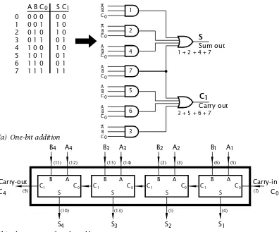
One of the first functions beyond simple gates to be integrated into a single IC was that of addition. The truth table of Fig. 2.7(a) shows the Sum (S) and Carry-Out (C1) resulting from the addition of the two bitsAandB and any Carry-In (C0). For instance row 6 states that adding two1s with a Carry-In of0gives a Sum of0and a Carry-Out of1(1+1+0=10). To im-plement this row we require to detect the pattern1 1 0; that isA·B·C0; which is gate 6 in the logic diagram. Thus we have by ORing all applicable patterns together for each output:
2. Logic Circuitry 23 P7 Q7 (17) (18) P7=Q7 (15) (16) P6 Q6 P6=Q6 (13) (14) P5 Q5 P5=Q5 (11) (12) P4 Q4 P4=Q4 (8) (9) P3 Q3 P3=Q3 (6) (7) P2 Q2 P2=Q2 (4) (5) P1 Q1 P1=Q1 (2) (3) P0 Q0 P0=Q0 (1) G Enable P=Q (19) 17 15 13 11 8 6 4 2 5 3 7 9 12 14 16 18 1 G1 7 0 P Q 0 7 1P=Q 19 [74LS688]
(a) Logic function (b) ANSI/IEC logic symbol
Fig. 2.6 The 74LS688 octal equality detector.
Using such a circuit for each column of a binary addition, with the Carry-Out from columnk−1 feeding the Carry-In of columnkmeans that the addition of any twon-bit words can be simultaneously implemented. As shown in Fig. 2.7(b), the 74LS283 adds two 4-bit nybbles in 25 ns. In practice the final Carry-Out C4is generated using additional circuitry to avoid the delays inherent on the carries rippling though each stage from the least to the most significant digit. n 74LS283s can be cascaded to implement addition for words of 4 × n width. Thus two 74LS283s perform a 16-bit addition in 45 ns; the extra time being accounted for by the carry propagation between the two units.
Adders can of course be coaxed into subtraction by inverting the min-uend and adding one, that is 2’s complementation. An Adder/Subtractor circuit could be constructed by feeding the minuend word through an array of XOR gates acting as programmable inverters (see page 14). The Mode lineAdd/Subin Fig. 2.8 that controls these inverters also feeds the Carry-In, effectively adding one when in the Subtract mode.
Extending this line of argument leads to the Arithmetic Logic Unit
A B C S C 0 0 0 0 0 0 1 0 0 1 1 0 2 0 1 0 1 0 3 0 1 1 0 1 4 1 0 0 1 0 5 1 0 1 0 1 6 1 1 0 0 1 7 1 1 1 1 1
0 1 AB
C 0 0 C A B 0 C A B 0 C A B 0 C A B 0 C A B 0 C A B Sum out Carry out S C1
(a) One-bit addition
C0 1 C A B S A B S 1 1 1 2 2 B A S S C1 B 2 0 C A 3 3 B A S S C1 B 3 0 C A 4 4 B A S S C1 B 4 0 C A Carry-in Carry-out
(b) The 74LS283 four-bit adder
(7) (9) (5) (6) (3) (2) (14) (15) (12) (11)
(10) (13) (1) (4)
1 2 4 7 5 6 3
1 + 2 + 4 + 7
3 + 5 + 6 + 7
C4 C0
Fig. 2.7 Addition.
addition and subtraction, the logic operations of AND, OR and XOR are supported. The 74LS382 even generates the 2’s complement overflow function (see page 10).
As we shall see, the ALU is the heart of the computer and micropro-cessor architectures. By feeding the Select inputs with a series of mode words, a program of operations can be performed by the ALU. Such
operation codesare stored in an external memory, and are accessed se-quentially by the computer’s control circuits.
2. Logic Circuitry 25
B1
2
B
3
B
4
B
A4 A3 A2 A1
0
C
ADD/SUB Word B
Word A
S1 S2 S3 S4
Sum/Difference
C4
Carry/Borrow out
Fig. 2.8 Implementing a programmable adder/subtractor.
0 0 0 Clear (F=0000) 0 0 1 Subtract (B-A) 0 1 0 Subtract (A-B) 0 1 1 Add (A+B) 1 0 0 EOR (A + B) 1 0 1 OR (A + B) 1 1 0 AND (A B) 1 1 1 Preset (F=1111)
Operation S2 1S S0
A3 A2 A1 A0 B3 B2 B1 B0 S2 S1 S0
F3 F2 F1 F0
Word A Word BMode Select S
Function Output F ALU
Carry-Out
Overflow
(17) (19) (1) (3) (16) (18) (2) (4) (7) (6) (5)
(12) (11) (9) (8)
(a) Function table (b) Logic diagram/pinning
C(n+4) OVR
(14) (13)
C(n)
(15) Carry-In
[74LS382]
Fig. 2.9 The 74LS382 ALU.
implement the 1-bit full adder of Fig. 2.7(a), but any two functions of three variables can be generated.
0
X/Y
1 2 4
1
2
3
4
5
6
7
G
A
B
C0
C1 S
CS
OE
0
1
0
1
0
0 1 1
1
1
1
1
0
1
1
+V
0 1
Output data Output Enable
Address Chip Select
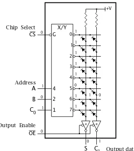
Fig. 2.10 A ROM-implemented 1-bit adder.
a high voltage, a selection of diodes could be taken out of contact. Such devices are called Programmable ROMs(PROMs).
2. Logic Circuitry 27 15 16 17 18 19 20 21 22 23 24 25 26 27 28 4 7 6 5 13 12 11 10 9 14 8 3 2 1 VDD PGM A8 A9 A11 OE A10 CE D7 D6 D5 D4 D3 VPP A12 A7 A6 A5 A4 A3 A2 A1 A0 D0 D1 D2 VSS A0 A1 A2 A3 A4 A5 A6 A7 A8 A9 A10 A11 A12
EPROM 8192x8
D0 A A D1 A D2 A D3 A D4 A D5 A D6 A D7 0 12 [POWER DOWN] & EN CS OE A 0 8191
(a) Dual in-line package (b) Logic symbol
[2764]
Fig. 2.11 The 2764 Erasable PROM.
are however, much cheaper to produce and are thus suitable for small to medium-scale production runs.
X
Y
VPP VDD G22 G21D2 S2 D1
S1 G1 TR2 TR1 Programmable element Addressable switch
Figure 2.12 shows a simplified representation of such a floating-gate MOSFET link. The cross-point device is a metal-oxide enhancement n-channel field-effect transistorTR1, rather than a diode. This MOSFET has its gate G1 connected to theX line and its sourceS1 to the Y line. If its drainD1were connected to the positive supply and theXline is selected (positive), then theYline too becomes positive (positive-logic1) asTR1is conducting (switch is on). However, ifTR1is disconnected fromVDDthen it does not conduct and the output on the Y line is logic 0. Transistor TR2 is in series with VDD and thus acts as the programmable element. TransistorTR2has an extra unconnected gate buried in the silicon diox-ide insulation layer. Normally there is no charge on this gate and TR2is off. If the programming voltage VPP is pulsed high to typically 20 – 25 V, negative charges tunnel across the extemely thin insulation surrounding the buried gate. This permanently turns TR2 on and thus connects TR1 to its supply. This shows up as a logic1on the Y line when selected by the internal memory decoder.
This charge remains more or less permanently on the buried gate un-til it is exposed to ultra-violet light. The high-energy light photons knock electrons (negative charges) out of the buried (floating) gate6 effectively discharging in around 20 minutes and wiping out all stored information. There are PROM structures which can be erased electrically, often in situe in the circuit. These are known variously as Electrically-Erasable PROMs (EEPROMs) or flash memories. In the former case a large negative pulse at VPP causes the captured electrons on the buried gate to tunnel back out. Generally the negative voltage is generated on the chip, which saves having to provide an additional external supply. Theflashvariant of EEP-ROM relies on hot electron injection rather than tunneling to charge the floating gate. The geometry of the cell is approximately half the size of a conventional EEPROM cell which increases the memory density. Pro-gramming voltages are also somewhat lower.
Most modern EPROM/EEPROMs are fairly fast, taking around 150 ns to access and read. Programming is slow, at perhaps 10 ms per word, but this is an infrequent activity. Flash EEPROM programs around 1000 times faster, in around 10µs per cell.
All the circuits shown thus far are categorised ascombinational logic. They have no memory in the sense that the output simply depends only on the present input, and not the sequence of events leading up to that input. Logic circuits, such as latches, counters, registers and read/write memories are described as sequential logic. Their output not only de-pends on the current input, but the sequence of prior inputs.
6This is called the Einstein effect. Einstein was awarded his Nobel prize for this
2. Logic Circuitry 29
R S Q 0 0 Q 0 1 1 1 0 0
(no change) (set)
(reset)
(a) Defining RS latch truth table
Q
Q
X 0 X 1
0 R
0 1 0
S
X 0
(c) Setting the latch (d) Resetting the latch X 0 0 1 0
S
R X 0
X 1
Q
Q 0
R
S R
S
Q
Q
(b) Logic symbol with true/complement outputs
Fig. 2.13 The R S latch.
Consider a typical door bell push-switch. When you press such a switch the bell rings, and it stops as soon as you release it. This switch has no memory.
Compare this with a standard light switch. Set the switch and the light comes on. Moreover it remains on when you remove the stimulus (usually your finger!). To turn the light off you must reset the switch. Again it remains off when the input is taken away. This type of switch is known as abistable, as it has two stable states. Effectively it is a 1-bit memory cell, that can store either an on or off state indefinitely.
A read-write memory, such as the 6264 device of Fig. 2.24, imple-ments each bistable cell using two cross-coupled transistors. Here we are not concerned with this microscopic view. Instead, consider the two cross-coupled NOR gates of Fig. 2.13. Remembering from Fig. 1.3(c) on page 13 that any logic1 into a NOR gate will always give a logic0 out-put irrespective of the state of the other inout-puts, allows us to analyse the circuit:
• If theSinput goes to1, then outputQ goes to0. Both inputs to the top gate are now 0 and thus output Q goes to 1. If the S input now goes backto 0, then the lower gate remains 0 (as theQ feedbackis 1) and the top gate output also remains unaltered. Thus the latch is set by pulsing theS input.
In the normal course of events – that is assuming that the R and S inputs are not both active at the same time7 then the two outputs are always complements of each other, as indicated by the logic symbol of Fig. 2.13(b).
S
R
Q
Q
+V
+V
Fig. 2.14 Using a R S latch to debounce a switch.
There are many bistable implementations. For example, replacing the NOR gates by NAND gives a R S latch, where the inputs are active on a logic0. The circuit illustrated in Fig. 2.14 shows such a latch used to de-bounce a mechanical switch. Manual switches are frequently used as in-puts to logic circuits. However, most metallic contacts will bounce off the destination contact many times over a period of several tens of millisec-onds before settling. For instance, using a mechanical switch to interrupt a computer/microprocessor will give entirely unpredictable results.
In Fig. 2.14, when the switch is moved up and hits the contact the latch is set. When the contact is broken, the latch remains unchanged, provided that the switch does not bounce all the way backto the lower contact. The state will remain Set no matter how many bounces occur. By symmetry, the latch will reset when the switch is moved to the bottom contact, and remain in this Reset state on subsequent bounces.
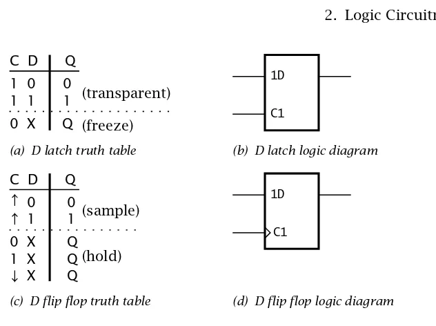
TheD latchis an extension to the R S latch, where the output follows the D (Data) input when the C (Control) input is active (logic1 in our example) and freezes when Cis inactive. The D latch can be considered
7If they where, then bothQandQgo to0. On relaxing the inputs, the latch will end up
2. Logic Circuitry 31
C D Q
1 0 0 1 1 1
0 X Q
(transparent)
(freeze) C1
1D
C D Q
0 0 1 1
0 X Q 1 X Q X Q
(sample)
(hold)
(a) D latch truth table (b) D latch logic diagram
(c) D flip flop truth table (d) D flip flop logic diagram
C1 1D
Fig. 2.15 The D latch and flip flop.
to be a 1-bit memory cell where the datum is retained at its value at the end of the sample pulse.
In Fig. 2.15(b) the dependency of the Data input with its Control is shown by the symbology C1 and 1D. The 1 prefix to D shows that it depends on any signal with a1suffix, in this case theCinput. That isC1 clocks in the1Ddata.
A flip flop is also a 1-bit memory cell, but the datum is only sampled on anedgeof the control (known here as the Clock) input. TheD flip flop
described in Fig. 2.15(c) is triggered on a / (as illustrated in the truth table as ↑), but \ clocked flip flops are common. The edge-triggered activity is denoted as on a logic diagram, as shown in Fig. 2.15(d).
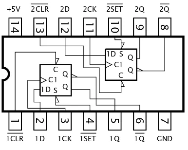
The 74LS74 shown in Fig. 2.16 has two D flip flops in the one SSI circuit. Each flip flop has an overriding Reset (R) and Set (S) input, which are asynchronous – that is not controlled by the Clockinput. MSI functions include arrays of four, six and eight flip flops all sampling simultaneously with a common Clockinput.
The 74LS377 shown in Fig. 2.17 consists of eight D flip flops all clocked by the same single Clockinput C, which is gated by input G. Thus the 8-bit data 8D…1D is clocked in on the / of C if G is Low. In the ANSI/ISO logic diagram shown in Fig. 2.17(b), this dependency is indi-cated asG1→1C2→2D, which states thatGenables the Clockinput, which in turn acts on the Data inputs.
1 2 3 4 5 6 7 8 9 10 11 12 13 14 C1 1D C S Q Q Q Q 1D C1 S C
+5V 2CLR 2D 2CK 2SET 2Q 2Q
GND 1Q 1Q 1SET 1CK 1D 1CLR S C1 1D R 4 3 2 1 5 6 10 12 11 13 8 9 [74LS74]
(a) Logic function (b) ANSI/IEC logic symbol
Fig. 2.16 The 74LS74 dual D flip flop.
latch outputs have a 3-state capability. This is useful if data is to be cap-tured and later put onto a common data bus to be read subsequently as desired by a computer.
A pertinent example of the use of a PIPO register is shown in Fig. 2.19. Here an 8-bit ALU is coupled with an 8-bit PIPO register, accepting as its input the ALU output, and in turn feeding one input word backto the ALU. This register accumulates the outcome of a series of operations, and is sometimes called anAccumulatororWorking register. To describe the operation of this circuit, consider the problem of adding two words A and B. The sequence of operations, assuming the ALU is implemented by cascading two 74LS382s might be:
1. Program step.
• Mode =000 (Clear).
• Pulsing Execute loads the ALU output (0000 0000) into the register.
• Data out is zero (0000 0000). 2. Program step.
• Fetch Word A down to the ALU input.
• Mode =011 (Add).
• Pulse / \ Execute to load the ALU output (Word A + zero) into the regi