Sekigaisen kogaku shisutemuyo shirikon porima fukugo renzu no kaihatsu
Bebas
174
0
0
Teks penuh
(2) DISSERTATION Submitted to the School of Integrated Design Engineering, Keio University, in partial fulfilment of the requirements for the Degree of Doctor of Philosophy. i.
(3) For my parents for supporting me to achieve big, and for my wife, Nor Arzuwin binti Ahmad and my childrens, Nurul Insyirah, Muhammad Irfan, and Muhammad Ilman, for their love, support, and sacrifices. ii.
(4) Table of Contents List of figures ..........................................................................................................................vii List of table ............................................................................................................................. xv Abstract .................................................................................................................................. xvi Acknowledgement .................................................................................................................... 1 CHAPTER 1. Motivation and introduction ....................................................................... 3. 1.1 Overview of issues regarding infrared lenses .............................................................. 3 1.2 Significance of the research ......................................................................................... 4 1.3 Research objectives ...................................................................................................... 5 1.4 Organization of dissertation ......................................................................................... 6 CHAPTER 2. Literature review .......................................................................................... 8. 2.1 Precision IR lenses fabrication..................................................................................... 8 2.2 Infrared imaging......................................................................................................... 11 2.3 Infrared lens material ................................................................................................. 13 2.3.1 Germanium ......................................................................................................... 13 2.3.2 Silicon ................................................................................................................. 14 2.3.3 Chalcogenide glass.............................................................................................. 15 2.3.4 High-density polyethylene .................................................................................. 15 2.4 Previous research works in the literature ................................................................... 17 2.4.1 Previous works on hybrid lens ............................................................................ 17 CHAPTER 3. Press molding of Si-HDPE substrate ........................................................ 22. 3.1 Introduction ................................................................................................................ 22 iii.
(5) 3.2 Si-HDPE substrate design .......................................................................................... 24 3.3 Mold design and fabrication ...................................................................................... 27 3.4 Press molding ............................................................................................................. 28 3.4.1 Experimental setup.............................................................................................. 30 3.4.2 Molding conditions ............................................................................................. 31 3.5 Si-HDPE substrate evaluation.................................................................................... 33 3.5.1 Si-HDPE adhesion .............................................................................................. 34 3.5.2 Si-HDPE interface phenomenon ......................................................................... 36 3.5.3 Infrared transmittance ......................................................................................... 42 3.6 Optical evaluation ...................................................................................................... 48 3.6.1 Optical evaluation setup ...................................................................................... 48 3.6.2 Optical evaluation ............................................................................................... 49 3.6.2.1. Image evaluation using chart ...................................................................... 50 3.6.2.2. Image sharpness evaluation ........................................................................ 51 3.6.2.3. Night mode imaging evaluation .................................................................. 53 3.7 Chapter summary ....................................................................................................... 55 CHAPTER 4. Microstructures forming on Si-HDPE substrate ..................................... 56. 4.1 Micro lens array ......................................................................................................... 56 4.1.1 Micro lens array design ....................................................................................... 57 4.1.2 Mold design and fabrication ............................................................................... 58 4.1.2.1. Mold without plunger ................................................................................. 58 4.1.2.2. Mold with plunger....................................................................................... 58 4.1.2.3. Lens array machining .................................................................................. 59. iv.
(6) 4.1.3 Press molding of micro lens array ...................................................................... 60 4.1.3.1. Molding conditions ..................................................................................... 61 4.1.3.2. Demolding with uncoated mold .................................................................. 62 4.1.3.3. Mold coating ............................................................................................... 65 4.1.4 Form accuracy and surface integrity of micro lens array ................................... 66 4.1.4.1. Form accuracy............................................................................................. 66 4.1.4.2. Viscosity measurement ............................................................................... 70 4.1.4.3. HDPE plate as raw material ........................................................................ 72 4.1.4.4. Surface integrity .......................................................................................... 74 4.1.5 In-situ observation .............................................................................................. 78 4.1.5.1. Experimental setup...................................................................................... 78 4.1.5.2. In-situ observation ...................................................................................... 79 4.1.6 Numerical simulation of pellets press molding .................................................. 83 4.1.7 Trench formation on coating surface .................................................................. 88 4.1.8 Press molding in vacuum environment ............................................................... 91 4.1.9 Form accuracy improvement by shrinkage compensation.................................. 92 4.2 Fresnel lens ................................................................................................................ 94 4.2.1 Fresnel lens design .............................................................................................. 95 4.2.2 Mold design and fabrication ............................................................................... 97 4.2.3 Press molding of Fresnel lens ........................................................................... 100 4.2.3.1. Experimental setup.................................................................................... 100 4.2.3.2. Molding conditions ................................................................................... 101 4.2.4 Form accuracy evaluation ................................................................................. 102 4.2.5 Numerical simulation of Fresnel press molding ............................................... 109 v.
(7) 4.3 Chapter summary ..................................................................................................... 112 CHAPTER 5. Infrared imaging evaluation .................................................................... 114. 5.1 Micro lens array ....................................................................................................... 115 5.1.1 Lens design evaluation ...................................................................................... 115 5.1.2 Imaging setup and image evaluation................................................................. 116 5.1.2.1. Image evaluation ....................................................................................... 118 5.2 Double Fresnel lens.................................................................................................. 118 5.2.1 Determination of refractive index ..................................................................... 119 5.2.2 Evaluation of lens design .................................................................................. 120 5.2.3 Imaging setup and evaluation ........................................................................... 125 5.2.3.1. Imaging setup ............................................................................................ 125 5.2.3.2. Lens performance evaluation .................................................................... 126 5.2.4 Night mode imaging ......................................................................................... 134 5.2.5 Thermography imaging ..................................................................................... 136 5.2.6 Combination of Si-HDPE with Ge lens ............................................................ 137 5.2.7 Si-HDPE and HDPE Fresnel lens comparison. ................................................ 139 5.3 Chapter summary ..................................................................................................... 140 CHAPTER 6. Conclusion ................................................................................................. 142. 6.1 Conclusion ............................................................................................................... 142 6.2 Future works ............................................................................................................ 143 References ............................................................................................................................. 145 List of Achievement ............................................................................................................. 155. vi.
(8) List of figures Figure 2.1: Schematic diagram of lens grinding process. .......................................................... 8 Figure 2.2: Schematic diagram of precision glass molding process. ......................................... 9 Figure 2.3: Schematic diagram of ultra-precision diamond lathe. ........................................... 10 Figure 2.4: Examples of IR imaging applications. .................................................................. 12 Figure 2.5: IR transmittance comparison of different IR substrates. ....................................... 13 Figure 2.6: An example of Ge lens for IR imaging. ................................................................ 14 Figure 2.7: Thin Fresnel lens for IR applications. ................................................................... 16 Figure 2.8: Hybrid glass-polymer UV curing process: (a) placement of UV resin and glass lens, (b) UV curing process, and (c) demolding. ......................................... 17 Figure 2.9: Glass-polymer hybrid lens fabricated using UV curing method. .......................... 18 Figure 2.10: Fabrication of glass-polymer hybrid by using injection molding: (a) a glass lens is inserted into the mold, (b) the mold is closed and polymer injected into the mold, (c) the mold is opened, and (d) the hybrid glass-polymer lens is completed. ......................................................................................................... 19 Figure 2.11: Fabrication of glass-polymer utilizing the compression molding process: (a)-(c) glass molding process, and (d)-(f) hybrid glass-polymer hot embossing.............................................................................................................. 20 Figure 2.12: A Si-glass hybrid lens.......................................................................................... 21 Figure 3.1: Si-HDPE hybrid substrate. .................................................................................... 22 Figure 3.2: IR transmittance of rough and polished Si. ........................................................... 25 Figure 3.3: Photograph of: (a) a laser-drilled Si, and (b) a broken piece of Si after press molding. ................................................................................................................ 26 Figure 3.4 Si-HDPE hybrid structure design. .......................................................................... 26. vii.
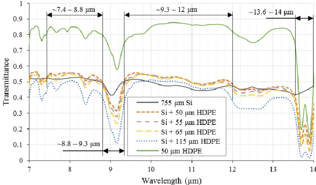
(9) Figure 3.5: Schematic diagram of upper and lower mold structure. ........................................ 27 Figure 3.6: Photographs of fabricated aluminium molds......................................................... 28 Figure 3.7: Schematic diagram of the glass molding press machine. ...................................... 29 Figure 3.8: Glass molding press machine. ............................................................................... 29 Figure 3.9: Schematic diagram of press molding process: a) material setup, b) heating, c) pressing, and d) cooling and specimen removal. .................................................. 30 Figure 3.10: Light diversion in a hybrid structure a) without a gap, and b) with a gap. ......... 31 Figure 3.11: Process parameters for the hybrid structure molding press. ................................ 32 Figure 3.12: Si-HDPE measurement using FTIR measuring instrument. ............................... 33 Figure 3.13: Photograph of the Si-HDPE hybrid substrate under melting temperature of 133 °C.................................................................................................................... 35 Figure 3.14: Photographs of the Si-HDPE hybrid substrates pressed under different heating times: a) 50 seconds, b) 60 seconds, and c) 70 seconds. .......................... 36 Figure 3.15: Photograph of two pressed HDPE-Si substrates, showing different sides. ......... 36 Figure 3.16: Positive and negative charges at the polymer-metal interface. ........................... 37 Figure 3.17: Cross-sectional SEM images of the interface of a hybrid substrate formed at 133 °C.................................................................................................................... 38 Figure 3.18: Enlarged view of Si-HDPE interface phenomenon showing the stretched HDPE. ................................................................................................................... 39 Figure 3.19: Cross-sectional SEM images of the interface of a hybrid substrate formed at 140 °C.................................................................................................................... 39 Figure 3.20: Enlarged view of the Si-HDPE interface. ........................................................... 40 Figure 3.21: Schematic of chemical bonding between substrate. ............................................ 40 Figure 3.22: Silane primer structures. ...................................................................................... 41 Figure 3.23: HDPE IR transmittance of different varying thicknesses. .................................. 42 viii.
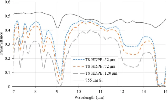
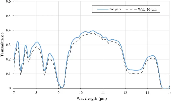
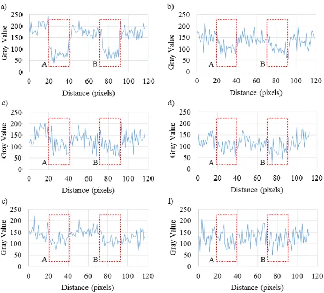
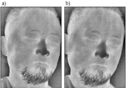
(10) Figure 3.24: IR transmittance of Si, HDPE, and Si-HDPE hybrid substrates with various HDPE thicknesses. ................................................................................................ 43 Figure 3.25: IR transmittance of Si etched with HF. ............................................................... 45 Figure 3.26: Photograph of two side laminated Si-HDPE hybrid substrates, showing different sides. ....................................................................................................... 46 Figure 3.27: IR transmittance of two side (TS) laminated Si with different varying HDPE thicknesses. ........................................................................................................... 46 Figure 3.28: Effect of an interface gap on the IR transmittance of a hybrid substrate. ........... 47 Figure 3.29: Effect of molding temperature on the IR transmittance. ..................................... 48 Figure 3.30: Camera setup with image chart for optical performance evaluations. ................ 49 Figure 3.31: IR images without filter and images for different substrates: b) 755 μm Si, c) 50 μm HDPE + 755 μm Si, d) 65 μm HDPE + 755 μm Si, d) 75 μm HDPE + 755 μm Si, and f) 155 μm HDPE + 755 μm Si. ................................................. 50 Figure 3.32: Image cross section for edge sharpness measurement. ....................................... 51 Figure 3.33: Image edge sharpness measurement: a) without filter, b) 755 μm Si, c) 50 μm HDPE + 755 μm Si, d) 65 μm HDPE + 755 μm Si, e) 75 μm HDPE + 755 μm Si, f) 155 μm HDPE + 755 μm Si. .................................................................. 52 Figure 3.34: HDPE thickness effect on the image’s gray value. ............................................. 53 Figure 3.35: Night mode images obtained by different lens substrates: a) 755 μm Si, and b) 50 μm HDPE + 755 μm Si. ............................................................................... 54 Figure 3.36: Night mode images obtained by 620 μm thick HDPE. ....................................... 54 Figure 4.1: Schematic diagram of: (a) Si-HDPE hybrid lens array design, and (b) lens cross section. ......................................................................................................... 57 Figure 4.2: Upper mold design without plunger. ..................................................................... 58 Figure 4.3: Upper mold design with plunger. .......................................................................... 59 ix.
(11) Figure 4.4: Photograph of (a) an aluminum mold insert with micro-lens array, and (b) three-dimensional topography of the mold. .......................................................... 60 Figure 4.5: Form error profile of a micro-lens dimple on the mold insert............................... 60 Figure 4.6: Photograph of: (a) lens array mold, (b) contaminated lens insert, and (c) contaminated formed lens. .................................................................................... 63 Figure 4.7: Photograph of (a) mold insert without coating, and (b) upper mold assembly with stripper ring. .................................................................................................. 64 Figure 4.8: Photograph of (a) adhesion of HDPE on the mold insert, and (b) tear off lens. ... 64 Figure 4.9: Layer structures of the mold insert coating. .......................................................... 65 Figure 4.10: Photograph of (a) coated mold insert, and (b) mold assembly. ........................... 66 Figure 4.11: Sag heights of lenses formed at different molding forces and different temperatures: (a) 133 °C, and (b) 140 °C, using the upper mold without a plunger. ................................................................................................................. 67 Figure 4.12: Sag heights of lenses formed at different molding forces and different temperatures: (a) 133 °C, and (b) 140 °C, using the upper mold with a plunger. ................................................................................................................. 68 Figure 4.13: Schematic diagram of: (a) press molding in a vacuum, and (b) press molding in a non-vacuum environment............................................................................... 69 Figure 4.14: Air trapping on lens apex. ................................................................................... 69 Figure 4.15: Lens sag heights for different HDPE thicknesses. .............................................. 70 Figure 4.16: Schematic diagram of a viscosity measurement unit. ......................................... 72 Figure 4.17: HDPE pellets to circular plate. ............................................................................ 73 Figure 4.18: HDPE circular plate mold assembly. .................................................................. 73 Figure 4.19: Sag heights of lenses formed at different molding forces using a HDPE circular plate. ......................................................................................................... 74 x.
(12) Figure 4.20: (a) Photograph of trench formation on a lens surface and (b) threedimensional topography of a Si–HDPE hybrid lens, showing an uneven lens surface. .................................................................................................................. 76 Figure 4.21: Air trap and trench formation under different pressing forces and temperatures. ......................................................................................................... 76 Figure 4.22: Air trapping phenomena at different HDPE thicknesses..................................... 77 Figure 4.23: Photograph of a cross-section of sliced molds. ................................................... 79 Figure 4.24: In-situ air trapping observation results at 133 °C. ............................................... 80 Figure 4.25: In-situ air trapping observation results at 140 °C. ............................................... 81 Figure 4.26: Schematic diagram of air trapping formation...................................................... 82 Figure 4.27: In-situ air trapping observation for a flat shaped HDPE. .................................... 82 Figure 4.28: Schematic diagram of the pellets press molding simulation setup. ..................... 83 Figure 4.29: Press molding simulation at the pressing temperature of 133 °C. ....................... 86 Figure 4.30: Press molding simulation at the pressing temperature of 140 °C. ....................... 87 Figure 4.31: (a) Surface of mold coating; (b) magnified view of rectangle (i) showing trench formation; (c) magnified view of rectangle (ii) showing worn out of coating; (d) magnified view of rectangle (iii) showing HDPE adhesion. ............. 89 Figure 4.32: Cross-sectional profile of a micro-lens dimple on the mold, showing worn out, HDPE adhesion, and trench formation areas. ................................................ 90 Figure 4.33: Three-dimensional topography of mold surface showing the wearing out of coating. .................................................................................................................. 90 Figure 4.34: Energy-dispersive X-ray fluorescence of coated mold insert. ............................ 91 Figure 4.35: A press molded Si–HDPE hybrid lens array in a vacuum environment: (a) center region, (b) outer region, (c) three-dimensional topography. ...................... 92. xi.
(13) Figure 4.36: Lens sag height obtained at different pressing forces in a vacuum environment. ......................................................................................................... 93 Figure 4.37: Photograph of two pressed Si-HDPE lens arrays, showing different sides......... 94 Figure 4.38: Collapsing spherical shaped lens into Fresnel shaped lens. ................................ 94 Figure 4.39: Si-HDPE hybrid Fresnel structures. .................................................................... 95 Figure 4.40: Schematic diagrams of Fresnel structure surface geometry. ............................... 97 Figure 4.41: (a) Photograph of an aluminum mold insert with a spherical Fresnel structure, (b)-(d) microscope images of the spherical Fresnel structure, (e) mold insert cross section of a spherical Fresnel structure obtained by UV curing, (f) photograph of an aluminum mold insert with an aspherical Fresnel structure, (g)-(i) microscope images of an aspherical Fresnel structure, and (j) mold insert cross section of an aspherical Fresnel structure obtained by UV curing. ............................................................................................................. 98 Figure 4.42: Measurement errors using non-contact measurement. ........................................ 99 Figure 4.43: UV curing replication process and cross-sectioning method. ........................... 100 Figure 4.44: Press molding process of a Si-HDPE hybrid lens: (a)-(c) hybrid substrate press molding, and (d)-(f) press molding of the Fresnel structure. ..................... 101 Figure 4.45: Zone depth change of the Fresnel structure for different temperatures under the pressing force of 0.2 kN. ............................................................................... 103 Figure 4.46: Microscope images of formed Fresnel lens under different pressing forces at a temperature of 130 °C................................................................................... 104 Figure 4.47: Zone height of the Fresnel under different pressing forces at a temperature of 130 °C. ............................................................................................................ 105 Figure 4.48: Microscope images of formed Fresnel lens under different pressing forces at a temperature of 131 °C................................................................................... 106 xii.
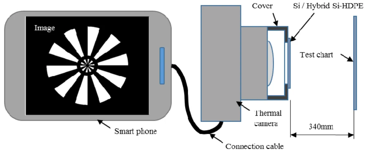
(14) Figure 4.49: Zone height of the Fresnel under different pressing forces at a temperature of 131 °C. ............................................................................................................ 107 Figure 4.50: (a) Cross-sectional profile of lens geometry, (b) a press molded Si-HDPE hybrid Fresnel lens and a Japanese coin. ............................................................ 108 Figure 4.51: (a) Cross-sectional SEM images of a Si-HDPE Fresnel lens; (b) magnified view of rectangle (i) showing the interface. ........................................................ 108 Figure 4.52: Schematic diagram of Fresnel press molding simulation setup. ....................... 109 Figure 4.53: Cavities filling of the Fresnel during initial press molding step. ...................... 110 Figure 4.54: Flat region formation of the Fresnel during press molding. .............................. 111 Figure 4.55: Complete filling of the Fresnel cavities. ........................................................... 112 Figure 5.1: Schematic diagram of focal length. ..................................................................... 115 Figure 5.2: Ray trace of microlens array. .............................................................................. 116 Figure 5.3: Microlens array imaging stage setup. .................................................................. 117 Figure 5.4: Photograph of (a) IR camera attached to the imaging stage, and (b) letter ‘E’ image masking. ................................................................................................... 117 Figure 5.5: Image of ‘E’ letter captured by using Si-HDPE micro lens array. ...................... 118 Figure 5.6: Refractive index of HDPE for different IR wavelengths. ................................... 120 Figure 5.7: Schematic diagram of a double Si-HDPE hybrid Fresnel lens system. .............. 121 Figure 5.8: Ray trace of the lens systems. ............................................................................. 123 Figure 5.9: Spot diagram at lens focal point. ......................................................................... 123 Figure 5.10: Zemax lens transverse ray fan plot for different wavelength and incident angles. ................................................................................................................. 124 Figure 5.11: (a) An original image from Zemax software and (b) simulated image obtained by the double Si-HDPE hybrid lens. .................................................... 125 Figure 5.12: Schematic diagram of IR imaging systems camera setup. ................................ 126 xiii.
(15) Figure 5.13: Camera setup for night imaging performance evaluation. ................................ 126 Figure 5.14: Diffractive limit of the double Si-HDPE hybrid Fresnel lens system. .............. 128 Figure 5.15: Square wave representative of the contrast. ...................................................... 129 Figure 5.16: Photograph of: (a) ImageMaster MTF equipment and (b) cross section measurement for different image height. ............................................................ 130 Figure 5.17: MTF measurement conditions. .......................................................................... 131 Figure 5.18: Comparison of geometric MTF calculated by Zemax and measured results for different field angles: (a) θ = 0°, (b) θ = 5°, (c) θ = 10°, and (d) θ = 15°. ..... 132 Figure 5.19: Zemax-simulated and measured image distortion. ............................................ 133 Figure 5.20: Schematic diagram of image distortion. ............................................................ 133 Figure 5.21: Focal length measurement results at a wavelength of 10 μm. ........................... 134 Figure 5.22: Visible light and night vision images at different distances; (a)-(b) 400 mm and (c)-(d) 2 m, and rectangle (i) showing image aberration. ............................. 135 Figure 5.23: Schematic diagram of stray light formation from the lens system. ................... 136 Figure 5.24: Thermography images of different lens systems: (a) standard germanium lens and (b) uncalibrated double Si-HDPE hybrid Fresnel. ................................ 137 Figure 5.25: (a) Schematic diagram of combining a Si-HDPE hybrid lens and germanium lens, (b) night vision images captured by combining a Si-HDPE hybrid lens and a germanium lens at different distances; (b) 400 mm and (c) 2 m, and rectangle (i) showing image aberration. .............................................................. 138 Figure 5.26: Image sharpness evaluation between double Si-HDPE hybrid Fresnel and a combination of a spherical Si-HDPE hybrid Fresnel (Lens 1) + Ge. ................. 138 Figure 5.27: A 250 μm Fresnel lens made by HDPE ............................................................ 139 Figure 5.28: Image comparison of the object captured by using (a) Si-HDPE hybrid Fresnel, and (b) HDPE Fresnel lens. ................................................................... 140 xiv.
(16) List of table Table 3.1: Si material properties .............................................................................................. 23 Table 3.2: HDPE material properties. ...................................................................................... 24 Table 4.1: Plano-convex lens array design parameters. ........................................................... 57 Table 4.2: Viscosity measurement parameters. ....................................................................... 71 Table 4.3: Stress-strain tabular data (Stress: MPa). ................................................................. 84 Table 4.4: Double Si-HDPE hybrid lens design parameters.................................................... 96 Table 5.1: Refractive index of Si ........................................................................................... 120 Table 5.2: Design results of lens unit..................................................................................... 122 Table 5.3: MTF measurement parameters. ............................................................................ 130. xv.
(17) ABSTRACT The demand for cost-effective infrared (IR) optics has increased over the past decade. Germanium (Ge) has been primarily used for the IR lenses because of its excellent IR transmittance and refractive index; however, Ge is bulky, heavy, and expensive. As an alternative, silicon (Si) is another IR material which is lighter and cheaper than Ge. However, as Si is a typical hard and brittle material, the ultraprecision machining of Si into complicated shapes like a Fresnel lens is considerably difficult. When diamond turning is used for machining Si, the process is very time-consuming, and serious tool wear takes place. In recent years, IR polymers, such as high-density polyethylene (HDPE), have been developed which are much cheaper and easier to shape by thermal molding processes. However, the transmittance of HDPE is still very low, thus the thickness of HDPE lens must be extremely thin, which brings the problem that the lens stiffness becomes very low and thus the substrate is easily deflected. Accordingly, there is an urgent need for exploring alternative IR substrate. In this study, a novel IR optical lens substrate, namely, the Si-HDPE hybrid substrate, was proposed and developed. An extremely thin layer of HDPE was laminated to one side of a Si wafer by means of silane-crosslinking, and the mechanical strength is further improved by utilizing a mechanical lock structure. Thus, the resulting Si-HDPE hybrid lens substrate possesses the advantages of both materials, i.e., the high stiffness and IR transmittance of Si together with the high formability of HDPE. The hybrid substrate was fabricated by highprecision press molding where the pressure and temperature were strictly controlled. The surface integrity and form accuracy of the developed Si-HDPE hybrid substrates were experimentally investigated. The IR imaging evaluation showed that the hybrid substrate was useable for night vision and thermography. The main contents of this study are summarized as follows: 1. Experimental results indicate that when the thickness of HDPE layer is less than 100 μm was attached to Si, the transmittance of Si is improved in ~7.4-8.8 μm and ~9.3-12 μm IR region. This is due to the HDPE layer acting as an anti-reflective coating of Si. The interface between Si and HDPE were evaluated and found that both substrates were successfully bonded with the aid of silane-crosslinking under controlled press molding parameters. The bonding of the two substrates occurs due to the chemical reactions at the interface. The bonding helps to eliminate the interface gap which affects the IR xvi.
(18) transmittance of the hybrid substrate. The press molding temperature also needs to be controlled as the use of a higher temperature degraded the HDPE and also reduced the IR transmittance. The developed Si-HDPE hybrid substrate was then optically evaluated, and it was revealed that the hybrid substrate was able to capture an IR images with acceptable image quality. 2. Press molding experiments were done, in which micro-lens structures were formed on the thin HDPE layer of the hybrid substrate. Two different lens structures were fabricated; micro-lens array and Fresnel lens. The micro-lens array was press molded at the polymer molten state in a non-vacuum condition. It was found that the air trapping occurs during press molding and caused severe damage to the lens surface and also affected the form accuracy. To investigate, a new in-situ direct observation was developed and used, and it is found that the air pockets were formed between the polymer pellets. Unescaped air during pressing caused the trench formation on lens surfaces which also reflects on mold coating. A numerical simulation conducted verified similar behaviour with the in-situ observation. As for that, pressing force should be kept to the minimum at the higher temperature to reduce the effect of air trapping to the surface integrities and lens accuracy. Press molding in a vacuum condition and shrinkage compensation were also conducted where the form accuracy and surface integrity were significantly improved. Meanwhile, in fabricating the Fresnel structures, a two-step molding method was applied. In the first step, a flat hybrid substrate was formed and the Fresnel structures were press molded in the second step to reduce the effect of air trapping. The form accuracy of the Fresnel was achieved at the higher pressing temperature and force. The experimental results also compared with the numerical simulation and the flow behaviour during press molding was studied. 3. Novel extra-thin Si-HDPE hybrid Fresnel lens was designed and evaluated to demonstrate the hybrid substrate’s usability for night imaging and thermography. The performance of the lens was measured and compared with simulated data, which showed good agreement. The night mode imaging trial also demonstrated the Si-HDPE hybrid lens usability as an IR systems lens where the object image at different distances was able to be captured. The thermography image was also captured, and the temperature distribution was shown. The Si-HDPE hybrid Fresnel lens also combined with Ge to show its ability to work with other lens material which resulted in clearer and sharper captured images. xvii.
(19) ACKNOWLEDGEMENT. Full praise and thanks to Allah the Almighty for making it possible for me to come to this point in life by granting me the good fortune to work on a Ph.D. research that I enjoyed at Keio University, one of the best institutions in Japan and for seeing me through the ups and downs through the journey that every Ph.D. degree brings about. Firstly, I would like to express my sincere gratitude to my advisor Professor Jiwang Yan for continuous support throughout my Ph.D. study and related research, for his patience, motivation, and immense knowledge. His guidance helped me in all stages of research and the writing of this thesis. I could not have imagined having a better advisor and mentor for my Ph.D. study. Besides my advisor, I would like to thank the rest of my thesis committee: Professor Norihisa Miki, Professor Masaki Omiya, and Associate Professor Takasumi Tanabe, for their insightful comments and encouragement, but also for the thought-provoking questions which gave me greater incentive to widen my research from various perspectives. My sincere thanks also go to Dr. Tsunetoshi Sugiyama, who continuously provided me with technical support during the research. Without his precious support, it would not be possible to conduct this research. Not to forget, many companies are also acknowledged: Global Wafers, Mitsubishi Chemical, Toshiba Machine, to name a few, for providing the samples and technical supports. A great source of motivation and inspiration for me has also come from my circle of friends here in Keio University – Atiq and Erialdi. I would also like to thank all of my 1.
(20) colleagues in the Precision Machining and Nano Processing Laboratory (Yan Lab), including Dr. Huang, Mukaida, Moriya, Yamasaki, Ishizuka, Niitsu, Takayama, and many others. The atmosphere in our laboratory was very inspirational and supportive throughout these years. I would like to reserve a very special gratitude, especially to my wife, Nor Arzuwin binti Ahmad, for always being very supportive with her encouragement, understanding, and for taking care of our children; Nurul Insyirah, Muhammad Irfan, and Muhammad Ilman, during my Ph.D. study. This dissertation is also dedicated to my family: my parents and to my brothers and sisters for supporting me spiritually throughout my studies and my life in general. Last but not the least, I would like to thank Keio Leading-edge Laboratory (KLL) for providing my research grant every year, making it possible for me to participate in overseas and domestic conferences in order to share the idea of my research to the public. Finally, the financial support from Malaysian Ministry of Higher Education and Universiti Malaysia Pahang towards my scholarship for all these years is gratefully acknowledged.. 2.
(21) CHAPTER 1. Motivation and introduction 1.1 Overview of issues regarding infrared lenses In recent years, the demand for IR optical imaging systems has risen, especially in night mode imaging and thermographic applications. High-end IR imaging requires good lens material and is often used in sophisticated technologies, primarily in the military. Meanwhile, the application of the IR optics in engineering, night driving assistance, security surveillance to name a few, are also demanding especially in mid to far IR region (7-14 μm). Recently, a new IR camera detectors which offer inexpensive detector are been developed [1]. This offers opportunities for the development of the cheaper IR camera system. Meanwhile, the current trend of the camera are also towards the miniature and compact system. However, due to the complicated and costly process of fabrication the IR lenses, the IR camera systems will remain out of the reach of the majority. It is due to the characteristic of some IR material which is hard to machine. If the manufacturing cost of the lens can be reduced, it is expected to reduce the cost of IR camera systems. Germanium (Ge), for example, possesses excellent transmittance rates in the mid-to-far IR region. However, it is bulky, heavy, and expensive [2]. Silicon (Si) is relatively lower in cost compared to Ge. It is also lighter, and in contrast, its IR absorbance is higher than that of Ge. However, machining both Ge and Si materials are difficult and expensive towing to their hard and brittle nature [3–6]. Ultraprecision machines and extremely sharpened diamond tools are 3.
(22) necessary to enable the ductile machining of Si and Ge. Machining the IR lens materials such as Ge and Si requires high precision and high stiffness machining. The machines must also be usable under a stable environment with strict temperature control and vibration isolation. In addition, the production cost is exorbitant because expensive single-crystal diamond tools are worn down very quickly especially when machining Si. These problems greatly limit the productivity and application of high-precision IR optics for everyday use. The polymer material is an alternative solution for expensive and difficult to machine substrates. High-density polyethylene (HDPE) offers a cheaper solution [7]. However, compared with Ge and Si, HDPE suffers from high IR absorbance and needs to be formed in very small thicknesses to obtain acceptable levels of IR transmittance. Thus, the stiffness level reduces and the substrate is easily deflected. A hybrid optical lens may work for visible light optical application [8,9]. It combines the various optical properties of the composing lens materials. Past research has demonstrated that a combination of glass and polymer can reduce the manufacturing cost, and improve the optical properties of the lens systems [10]. With that, it is believed that combining HDPE with Si will enable it to be used as IR substrate. The HDPE can be formed as a thin layer and attached to the Si. The Si will retain the shape of the HDPE layer; nevertheless different IR properties of the material can be selected and combined. The lens structures can be formed on the HDPE layer using a thermal shaping process. Thus, a cheaper solution of IR lens can be fabricated.. 1.2 Significance of the research Although it is possible to develop the Si-HDPE hybrid substrate/lenses by using press molding, the adhesion between the Si and HDPE need to be developed. However, the use of silane crosslinking polymer make it possible to be realized in which tenth of micron HDPE. 4.
(23) thickness can be attached to the Si. The thickness of the polymer was determined to achieve higher IR transmittance. As the press molding of the lens structures on the thin HDPE layer of the hybrid substrate is not reported in any literature, this research demonstrated the ability of the hybrid substrate to be formed precisely into an IR lens. Furthermore, the development of in-situ direct observation in this research also clarified the air trapping phenomenon due to the used of the HDPE pellets during press molding. This research also demonstrated the capability of the Si-HDPE hybrid lenses for IR imaging including thermography in which the temperature distributions are measured. Furthermore, this research aims to contribute towards lowering the manufacturing cost of fabricating IR lenses, thereby helping realize thin and compact IR imaging systems.. 1.3 Research objectives The objectives of this research are as follows: 1. To fabricate a Si-HDPE hybrid substrate/lens for IR applications for the wavelength of 7-14 μm. The adhesion method for Si and HDPE also needs to be developed. The gap between the substrate needs to be eliminated during the bonding process failing which it could detriment the IR transmittance. The interface phenomenon of the substrate also needs to be investigated. 2. To evaluate and determine the resulting IR properties of varying HDPE thicknesses of the hybrid substrate, and the image quality of the hybrid substrate with various HDPE thicknesses, respectively. 3. To form the lens structures on the thin layer of HDPE of the Si-HDPE substrate utilizing the press molding method. Also, to show the viability of forming the lens structures of the hybrid substrate using press molding, and to define the best process parameters.. 5.
(24) 4. To investigate the air trapping phenomenon during process needs, especially as the press molding is done in a non-vacuum condition. Also, to develop a new in-situ online observation method to study the formation of air trapping between the polymer pellets. 5. To design the lens using the Si-HDPE hybrid substrate to be used for IR application. Also to show the viability of the hybrid lens for IR imaging systems applications. 6. To verify the performance of the designed lens in the IR imaging, by developing home build testing equipment. Also to measure the lens performance, and the image quality was also evaluated. The possibilities of combining the Si-HDPE hybrid lenses with other lens material will also be examined.. 1.4 Organization of dissertation Chapter 1 provides the introduction and overview of the issues regarding research. The research significance and also the research objectives were included in this chapter. Chapter 2 provides an overview of lens fabricating techniques, as well as the IR imaging systems and the materials normally used in fabricating the IR lens. In this chapter, a method that past researchers used for fabricating a hybrid optical lens was detailed as well. Chapter 3 details the initial steps of fabricating the Si-HDPE hybrid lens. The method of combining the HDPE to the Si, and the interface phenomenon between Si and HDPE, and the IR evaluation and optical abilities of the hybrid substrate is explained in this chapter. In Chapter 4, contains the fabricating processes of forming microstructures on a HDPE layer of the hybrid substrate The mold design and machining methods are included in this chapter. Chapter 4 also examines the effect of the press molding parameters in maintaining surface integrities, and for accuracies of the microstructures, including the coating. The in-situ observation of air trapping phenomenon during the press molding is also detailed here. In 6.
(25) addition, a numerical simulation also described as well. A press molding in a vacuum environment and the resulting results of the form accuracy and surface integrities of the microstructures are also included in this chapter. Also, the formation of a Fresnel shaped out of Si-HDPE lens, and the mold fabrication prior to the press molding processes were explained. Chapter 5 delineates the lens and IR imaging evaluations respectively. The lens design and analysis are provided to show the performance of the designed lens. The lens performance was measured, and it was compared to simulated data. The formed lenses were tested using a home built imaging system, during which, the captured night mode and thermography images, demonstrated the designed and fabricated lens’s ability to visualise objects during the IR imaging. The combination of the different IR lens materials was also introduced in this chapter to examine the compatibility of the Si-HDPE hybrid lens with other lens material. Chapter 6 consists of the overall conclusion of the research. The future of this research area is also included.. 7.
(26) CHAPTER 2. Literature review 2.1 Precision IR lenses fabrication An infrared lenses are usually made from hard and brittle materials such as silicon and germanium. These materials had to experience a complicated shaping process in order to transform them into a final shape. A conventional method that involves three steps, particularly grinding, lapping, and finishing are imperative procedures for the transformation [11,12]. This method can be used to form a single lens and derive a good surface finish. However, it is inefficient to produce the complicated lens shapes in a large quantity that can be costly and time-consuming. The worst of it is the use of cutting fluid in the process is detrimental to our environment. Figure 2.1 illustrates a schematic diagram of the precision lens grinding process.. Figure 2.1: Schematic diagram of lens grinding process. 8.
(27) Precision glass molding process (GMP) is a prominently used method to fabricate the optical lenses at lower cost [13–15]. This lens molding process involves heating and cooling. During the thermal process of the molding, the glass is heated to the glass transition point with the aid of the IR heater, and subsequently it forms a viscoelastic material. Then, the nitrogen gas is used to cool down both mold and lens after the lens are press molded. This process is effective to produce the glass lenses, and obtain the accuracy and excellent surface finish of the lenses. The schematic process of the GMP is illustrated in Figure 2.2.. Figure 2.2: Schematic diagram of precision glass molding process. Chalcogenide glass is considered as an alternative material for the IR lenses [16]. Similar to a visible light glass lenses, it can be molded by using the GMP process effectively while the form accuracy can also be obtained. The chalcogenide glass can be heated above the softening point, pressed, and finally cooled. However, it is very sensitive to the molding process because the parameters of the GMP can influence the lens performance. This material 9.
(28) is subjected to the changes in refractive index due to the stress during molding [17]. During the GMP process, precaution measures need to be taken against the negative effects the glass will bring to the environment. It is due the chemical contents of the chalcogenide glass which contains hazardous and poisonous chemical for example arsenic. Therefore, the glass should be molded in vacuum surrounding to minimise the effect. Another major issue of this process is the long thermal cycles. The mold is also subjected to the thermal expansion that shortens the life span of the mold. This is a departure for many researchers to conduct their studies experimentally and numerically in response to this issue. Although the glass molding process is advantageous to the formation of the glass lenses, it is not applicable to silicon and germanium which require a higher softening point of both substrate. Given that the maximum operating temperature of the GMP is 800 °C, the softening point of more than 800 °C is mandatory to both silicon and germanium.. Figure 2.3: Schematic diagram of ultra-precision diamond lathe. Ultra-precision diamond lathe machine enjoys scholarly attention being the lens manufacturing method [4,6,18]. An aspherical to micro-lens array can be fabricated by using 10.
(29) this machine with a high accuracy and surface finish. With a combination of diamond point tools and slow tool servo systems, the machine eases the entire lens cutting process. This machine also enables the production of different shapes of the lens with the support of computer numerical code (NC) generation. The schematic diagram of the ultra-precision diamond lathe is shown in Figure 2.3. Although ultra-precision machining can produce different forms of lens, it still suffers from inevitable drawbacks. This method is similar to the conventional grinding and lapping process, which does not have the function to manufacture hard materials. As Si and Ge are hard and brittle, the cost incurs is much higher when adopted to fabricate lens from these two materials in a mass production. In fact, machining Ge is easier than machining Si [19]. A ductile mode cutting must be activated during the process to ensure that the precision and higher surface finish to be obtained. In the similar vein, the use of the diamond pointed tool also incurs higher fabrication cost. However, the lens cutting process may cause the machine to be easily worn out that reduces the machining efficiency.. 2.2 Infrared imaging A body with a temperature above the absolute 0 °C will release radiation energy or electromagnetic (EM) radiation. When EM is released, radiation is distributed from the body, the rate of which depends on the temperature of the body. The radiation that is emitted from the body is also called emissivity, which functioned as an IR wavelength [20]. The IR wavelength consists of, near-IR, mid-IR, and also far-IR. The maximum radiation energy, which depends on body temperature, can be calculated using Plank’s equations: 𝑊(𝜆, 𝑇) = 𝑒(𝜆)𝐶1 /𝜋𝜆5 [exp (. 𝐶2 ) − 1] 𝜆𝑇. (2.1). 11.
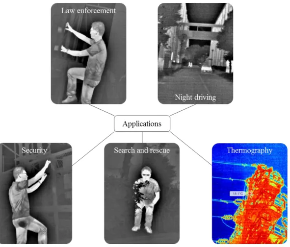
(30) where W (λ, T) represents the wavelength radiance in μm; and temperature in Kelvin (K). Meanwhile, the radiance, C1 is 3.7418 × 10⁸, and C2 is 14387.9 in units of watts m-2 steradians1. μm-1, which are constant for the equation. The emissivity of a wavelength which is varied in. the range of 0 to 1, is represented by e (λ). A special devices or systems is required to capture the body emissivity, which cannot be captured by the normal invisible camera. Individuals with normal eye-vision lack the ability to view of 0.4 – 0.7 μm light [21]. However, this view can be captured using an IR camera equipped with the cooled or uncooled image sensor. A special lens material is also attached to the camera, which can transmit the IR from the object body to the camera sensor via the lens. In fact, anything which emits the heat from the body can be captured with IR imaging systems. Figure 2.4 showed some of the applications of the IR camera.. Figure 2.4: Examples of IR imaging applications. 12.
(31) 2.3 Infrared lens material IR material can be made conventionally from several types of material. These materials are usually either made from semiconductors or crystalline. Germanium (Ge) and silicon (Si) are examples of semiconductor material. Some of the lenses are also made from a glass, for instance the chalcogenide glass (Ch). The aforementioned substrates will offer different characteristic of IR properties, each with different applications. This is displayed in Figure 2.5. These materials have their own advantages, drawbacks. The details of the IR material will be discussed after this section’s sub-topics.. Figure 2.5: IR transmittance comparison of different IR substrates. 2.3.1 Germanium Germanium (Ge) a semiconductor material, is very popular as IR lens material. It has high permeability and a high refractive index, the latter of which is around 5.76. Meanwhile, it has stable and good transmittance in the IR region of 2-14 μm. Thus, it is an excellent candidate for infrared lenses substrate material.. 13.
(32) Ge is relatively expensive, bulky, and heavy. Machining Ge into a flat and thin Fresnel shape appears to be the appropriate solution for reducing its weight [4]. However, fabricating the germanium into the final shape of the lens is a difficult and time-consuming process, and the resulting lenses are expensive. During heat exposure, Ge becomes opaque at about 400 °C, while its transmittance decreases by a factor of 2 at a temperature above 120 °C. Figure 2.6 shows an example of IR lens made from Ge.. Figure 2.6: An example of Ge lens for IR imaging. 2.3.2 Silicon Silicon (Si) is a popular material for electronic and photonic applications as it is costeffective [22]. It can be found in rocks, sand, clay and soil, as well as in other elements such as silicates. In its oxide or silicate form, it can be used to makes glass. Si is a brittle material and is used in many industries. It has become popular for optical components such as IR lenses and thermal imaging cameras. Si has a high transparency for far infrared (FIR) and is opaque for visible light. It also has excellent optical properties and thermal conductivity. The refractive index of Si is ~3.5. Although silicon can be used in IR optical applications, it has its own set of limitations. Reflectance is one of the problems, and although anti-reflective coating can be used to solve the issue, nevertheless the coating is not always appropriate for infrared optical systems [23]. 14.
(33) Meanwhile, the IR transmittance depends on the thickness of the Si. A significantly higher IR transmittance is recorded when the thickness of Si is less than 1 mm [24]. Si costs less than Ge, and the former is also light. However, to mold Si into the final shape of the IR lens, a precision machining is required. Ductile mode machining needs to be used when machining this kind of material. Specifically, an extremely sharp diamond point tool is required to make sure the ductile machining mode is realized. Typically, however, the diamond tools gets worn out very quickly due to the Si characteristics itself. Another method Si can also be shaped using an etching process. Nevertheless, the process is very timeconsuming making it an unpopular choice. 2.3.3 Chalcogenide glass Recently, chalcogenide glass has received a considerable amount of as suitable IR lens material. Chalcogenide glass has excellent IR transmission in the mid to long IR [16]. It offers a cheaper solution compared to Ge. The former’s refractive index ( ~2.5 ) is slightly higher than Si and slightly lower than Ge [25]. The forming process is considerably cheaper, as the lens shape can be formed using molding processes, especially using the glass molding press machine [26–28]. However, molding this particular type of material is hazardous, due to the contents of the material, which include arsenic and selenium. The only relatively safe ingredient of the glass is sulphur. 2.3.4 High-density polyethylene Although there are many types of polymers that reportedly can be used for optical systems, not all of them are suitable for IR applications. Polycarbonate (PC) and acrylic, for example, are good for visible light as owing to their optical clarity [29,30]. However, in IR light, this polymer is opaque, wherein IR is absorbed by the material. The IR absorption of the 15.
(34) polymer is due to the molecular vibration that occurs when IR light passes through it [31]. Specifically, it is because the normal polymer has light elements of carbon, hydrogen, and oxygen, wherein higher vibrational frequencies occur. The use of the polymer allows several thermal fabrication methods to be used to form the lens into its final shape; for instance by using injection molding and hot embossing. Unlike Ge and Si, the polymer can be heated into a softened state, before undergoing hot embossing. The polymer can be melted inside the injection molding barrel before being injected into the mold. The polymer then changes to the solid state after being hot embossed or being used in injection molding. When cooled the final product will be easily obtained. High-density polyethylene (HDPE) is the most suitable material to be used as IR material; this has been reported over 4 decades ago [32]. It is commonly available and used in various industries. HDPE’s good IR transmittance, in 6-14 μm region, is significantly higher than most polymers [33]. Previous research has highlighted the use of this material as an IR lens [34]. However, it still suffers higher from IR absorbance and needs to be formed into a very thin lens so as to compensate for the IR losses. Figure 2.7 displays a 300 μm thick Fresnel lenses, to compensate for IR absorbance.. Figure 2.7: Thin Fresnel lens for IR applications.. 16.
(35) 2.4 Previous research works in the literature In fabricating hybrid optics, several methods are utilized by the previous researchers. Various types of optical materials were attached, mainly to improve the lens performance, as well as to reduce the manufacturing cost. For instance, the achromatic lens, which is a lens consisting of different optical materials, which were combined to form a hybrid lens. 2.4.1 Previous works on hybrid lens Ultraviolet (UV) curable resin was the earliest method used to fabricate a hybrid lens whereby the resin was applied to the substrate, and subsequently it was cured by UV light [35– 38]. Before the UV curing (hardening) process starts, a suitable amount of UV resin is placed within the lens mold. After that, the glass lens is placed on the top of the UV resin, while the resin is cured with the aid of UV light. As a general rule, the glass lens or the mold must be UV light transparent to ensure that the UV light can be transmitted in order to harden the resin. The process of UV curing resin is illustrated in Figure 2.8, whereas an example of a hybrid glass-polymer is illustrated in Figure 2.9. This method provides a strong adhesion between the two materials.. Figure 2.8: Hybrid glass-polymer UV curing process: (a) placement of UV resin and glass lens, (b) UV curing process, and (c) demolding. 17.
(36) . Figure 2.9: Glass-polymer hybrid lens fabricated using UV curing method. Despite the usefulness of UV curable method, the curing process is indubitably complicated. The curing needs to be controlled properly as excessive UV power can cause the UV material to crack [37]. Due to the use of liquid UV resin, the air trapping is another problem in the process [39]. After pouring the UV resin into the mold, the resin will expose the material to the air trapping phenomenon, and thus it is strongly advisable to perform the process in a vacuum condition. However, the use of this method for producing hybrid IR optics is impossible because UV resin cannot transmit the IR. To date, there is no research done on the use of the UV resin as IR lenses. Another method used to fabricate a hybrid glass-polymer lens is injection molding. This method has a special design of the injection mold which controls the lens’s characteristics. To use this method, the glass is first inserted into the mold, then the molten polymer is injected to cover one side of the glass [10], as described in Figure 2.10. However, no adhesive agent is used in the injection molding process. The resulting lens assembly is held by the flange of the polymer lens. Most importantly, this process can produce the lens in a large quantity at cheaper cost with lower time cycles. A similar process is used to fabricate a silicone-glass hybrid lenses for photovoltaic application [40].. 18.
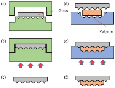
(37) Figure 2.10: Fabrication of glass-polymer hybrid by using injection molding: (a) a glass lens is inserted into the mold, (b) the mold is closed and polymer injected into the mold, (c) the mold is opened, and (d) the hybrid glass-polymer lens is completed. To guarantee a mass production of the lens, a multi mold cavities can be implied to the injection mold to allow the production of multiple lens in one injection molding cycle. Still, the injection molding suffers from some shortcomings. The effect of polymer flow will reduce the performance of the lens [10]. Hence, care should also be taken in designing the mold, especially the gate size and location where the polymer enters the lens cavity after being injected through the machine nozzle. When the hybrid lens are manufactured through this process, a weak adhesion exists between the two lens substrate due to the shear force between the substrate at the cooling stage. Figure 2.11 exhibits the compression molding process, which is another method used to fabricate glass-polymer hybrid lens. Through this method, a glass lens is molded and used as the lower cavity then. After that, the polymer is inserted on the top of the glass to be heated 19.
(38) and pressed. The polymer is adhered to the glass by heating and cooling the polymer during compression. The adhesion can be improved by applying hot glue between the two substrates [41]. In general, the compression molding process is similar to the GMP process. It enhances the efficiency of molding the optical lenses. The control of the pressing force can improve the adhesion between the two different substrate during the molding process. Concurrently, it can reduce the effect of shear force on the interface of the substrate.. Figure 2.11: Fabrication of glass-polymer utilizing the compression molding process: (a)-(c) glass molding process, and (d)-(f) hybrid glass-polymer hot embossing. A combination of glass and Si for simultaneous visible and infrared imaging has also been performed, whereby the glass is placed at the centre of a Si lens without any adhesion [42]. The combination of the Si and the glass for this application is showed in Figure 2.12. Undeniably, the fabricating process is challenging. This is because the time-consuming etching process is utilized to fabricate the Fresnel lens, which are made of silicon. Nevertheless, the quality of the surface finish produced through this method is considered poor as compared to other lens forming methods.. 20.
(39) Figure 2.12: A Si-glass hybrid lens. Attaching a polymer onto Si has been reported previously, and the adhesion of the polymer substrate to the Si was done with the help of the chemical process. In the present study, an adhesion chemical was applied to the Si, and the polymer was attached. The diamond turning was then used to cut the polymer into the final lens shape [43,44]. It should be added that, in using the adhesion between these two materials, care should be taken in choosing the appropriate adhesion material. This is because the adhesion material used must be able to transmit the IR light. A chemically attached polymer to the silicon helps to improve the adhesion between the two materials. However, it involves several process starting with the adhesion process and ends with the cutting process. During the adhesion process, the uniformity of the adhesion need also to be considered. On contrary, the ununiformed adhesion process creates an interface gap between the two substrate that allows the light to be reflected on the interface gap, and eventually the lens performance reduces. The interface phenomenon is not reported.. 21.
(40) CHAPTER 3. Press molding of Si-HDPE substrate 3.1 Introduction In this study, a Si-HDPE substrate is fabricated. A HDPE layer is attached to one side of the Si, as illustrated in Figure 3.1. The HDPE thickness is formed in a varying thicknesses to investigate the effect of these variations on the IR transmittance of the hybrid substrate. To attach the HDPE to the Si, no adhesion promoter is used, and the attaching process is done in melt condition of the HDPE.. Figure 3.1: Si-HDPE hybrid substrate. In this study, a glass molding press (GMP) machine is used as a press molding to form the Si-HDPE hybrid material. The molding temperature and pressure is precisely controlled in order to ensure that the shape transferability, surface quality, and interface strength can be improved [45,46]. Glass is normally formed at high temperatures (~500°C) which are above the glass transition temperature. At this point, the glass is in its softened state. In this study, as the HDPE polymer exhibits a lower softening temperature (125°C) and a lower melting point (133°C). Therefore, forming the Si-HDPE hybrid structure is more easily done in the melt state of HDPE, which is similar to that used in other applications [47]. Forming the polymer in its. 22.
(41) melt state is also beneficial for complete replications of microstructures or complicated shapes to the polymer, without damaging the mold and the thin Si substrate. Moreover, forming the Si-HDPE in the melt state also helps to create strong Si-HDPE adhesion during the press molding process. In the experiments, two types of materials were used. The first is single-crystal Si with 755 μm thickness in the form of a two-side polished wafer, which was provided by Global Wafers Japan Co. Ltd.. The properties of the Si material are displayed in Table 3.1. The Si wafer is then cut to the size of 15 mm × 15 mm using a diamond pen. Cylindrical HDPE granules with resin/pellets size of ∅3 mm × 3.5 mm, supplied by Mitsubishi Chemical Corporation, Japan, were used in the experiments. The grade of the HDPE material is LINKLON HM600A, which is a silane cross-linkable resin. This type of HDPE was selected because of its adhesive ability to Si. Table 3.1: Si material properties Material properties Type. Value P. Doping element. Boron. Resistance, Ω.cm. 27. Surface orientation. (111). Thickness, μm. 755. Refractive index. 3.5. Surface roughness (Ra), nm. 3.5. The properties of the HDPE granules are displayed in Table 3.2. The utilization of a silane cross linkable, such as HDPE does not require an adhesive because of its ability to create a direct bond between non-polar surfaces [48,49]. Crosslinking is a type of polymerization. 23.
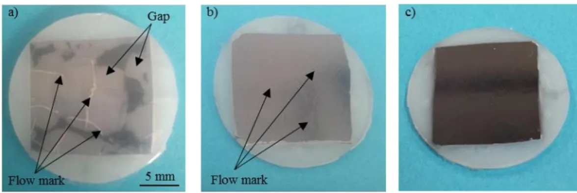
(42) reaction in which branching occurs out from the main molecular chain to form a network of chemical links. Table 3.2: HDPE material properties. Material properties. Value. Density, g/cmᵌ. 0.955. Melting point, °C. 133. Softening temperature, °C. 125. Shape. Granules. Grain size, mm. ∅3 × 3.5. Melt flow rate (190℃,21.2N), g/10min Refractive index. 9 1.5. 3.2 Si-HDPE substrate design To attach the HDPE layer to Si, several methods were developed. As the Si used in the experiment is polished, the HDPE does not adhere very well. Roughening the Si surface improves the adhesion of the two substrates. However, doing so will scatter the IR light when it is passing through an uneven surface of the Si substrate. The effect of the rough surface on the IR transmittance of the Si can be viewed in Figure 3.2, where is demonstrated that polished Si would result in higher IR transmittance. To improve the adhesion between HDPE and Si, a mechanical lock is considered, simply by securing the assembly using strong locking devices [50]. The mechanical lock or coupling was the earliest method introduced by MacBain almost 9 decades ago [51]. The shape irregularities or undercuts will become the mechanical coupling to attach the different substrate. The shape irregularities or undercuts become the mechanical couplings to attach the differing substrate. By considering this, research implemented the locking idea, to improve the adhesion between HDPE and Si. 24.
(43) Figure 3.2: IR transmittance of rough and polished Si. To create surface irregularities in some area of the Si surfaces, the used of drilled holed was considered. The first trial was conducted by drilling a hole into the Si using a laser. The HDPE layer is then created by heating and pressing it onto the Si. During pressing, the molten HDPE flows into the drilled hole to become the mechanical lock for both substrates. However, it is found that the Si is easily broken after the press molding process, especially at the laser drilled holes. This leads to micro-cracks around the hole. The micro cracks are then subjected to a pressing force during the press molding, and this causes the Si to break. Thus, the laser drilling method is not suitable for this study. The sample of the Si-HDPE hybrid substrate that uses laser drilling holes as its locking is shown in Figure 3.3.. 25.
(44) Figure 3.3: Photograph of: (a) a laser-drilled Si, and (b) a broken piece of Si after press molding. The structure of the Si-HDPE hybrid structure test piece was improved, and this is schematically shown in Figure 3.4. In the design of the hybrid substrate, the HDPE laminates one side of the polished Si, and the adhesion of the HDPE to the Si is carried out via crosslinking. As mentioned above, in order to improve the adhesion strength between the two materials, a mechanical lock (undercut) was designed at the edge of the Si substrate, leaving an effective lens area of 13 mm × 13 mm, after subtracting 1 mm for locking. In this way, the fragile Si substrate is fully protected by the HDPE from external shocks. Furthermore, the flatness of the HDPE film can be firmly maintained by the Si substrate.. Figure 3.4 Si-HDPE hybrid structure design. 26.
(45) 3.3 Mold design and fabrication Aluminum was selected as the material for the mold due to it being malleable in the machining process. As the HDPE polymer is also soft, the strength of aluminum is sufficient to prevent mold deflection. Next, the upper mold used in this study was shaped by using a universal lathe from an aluminium cylinder, to a diameter of ∅40 mm and a height of 20 mm. The top surface of the mold was then flattened/micro-structured using an ultraprecision lathe, NanoForm X (Ametech Precitech Inc., USA). The machine was equipped with an air bearing spindle and a single crystalline diamond tool, with a nose radius of 250 μm. The final mold surface had a mirror finish, with a surface roughness of 7.8 nm Ra.. Figure 3.5: Schematic diagram of upper and lower mold structure. The lower mold comprises of a group of elements, as is schematically shown in Figure 3.5, to form a flexible mold cavity. This is essential to control the shape of the HDPE material and create the mechanical lock for the Si-HDPE hybrid substrate. The cavity formed by the circular ring has a diameter of ∅22 mm, whereas the depth is automatically adjusted by a spring supporting the ring in accordance with the varying HDPE thickness. A stop bolt was put in 27.
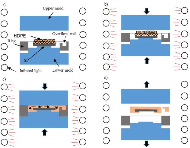
(46) place prevent the circular ring from dislodging itself from the mold. A photograph of the molds are displayed in Figure 3.6.. Figure 3.6: Photographs of fabricated aluminium molds.. 3.4 Press molding A glass molding machine GMP211 (Toshiba Machine Co. Ltd., Japan) was used for the press molding process of the Si-HDPE hybrid substrate. The machine was not equipped with a vacuum system. Instead, it contained a transparent silica glass tube chamber, which holds the purging nitrogen gas during molding. This prevents the oxidation of the molds at high temperatures. The machine structure is illustrated in Figure 3.7. The molds are usually attached to the heat isolator, which is made from ceramic. There is no moving component at the fixed upper mold system. Meanwhile, the lower mold is attached to the lower system of the machine. It has a moving Z-axis, which is moved in the upwards direction (+ve) when the press molding takes place. The molding temperature can rise to 800 °C with a ±1 °C tolerance level and is monitored by a thermocouple. The pressing force of the machine ranges from 0.2 kN to the maximum of 20 kN with a 0.98 N resolution. An AC servomotor controls the lower mold’s movement. 28.
(47) accuracy towards the stationary upper mold, with a resolution of 0.1 μm. Figure 3.8 displays the glass molding press machine.. Figure 3.7: Schematic diagram of the glass molding press machine.. Figure 3.8: Glass molding press machine. 29.
Gambar
+7
Dokumen terkait
The analyses compared workers of these three religious groups on the following: (i) perceptions of workplace safety, (ii) compliance with safety management
Paradigma penelitian dapat diartikan sebagai pola pikir yang menunjukkan hubungan antar variabel yang akan diteliti yang sekaligus mencerminkan jenis dan rumusan
diperlukan pada jembatan balok-T lebih ekonomis dari pada jembatan box culvert.. Kata kunci : jembatan, box culvert , balok-T, bangunan
Bahwa sanksi hukum yang ditimbulkan cyber sex akan berbeda pada setiap Negara, di Indonesia cyber sex dapat menimbulkan suatu pertanyaan yang berkenaan dengan hukum, jika media
Tujuan dari penelitian ini adalah untuk (1) mendapatkan formulasi terbaik untuk organogenesis aksis bunga pisang (AA, BB, AAB dan ABB), (2) mengetahui pengaruh
SecaI'a Ul11um diketahui bahwa pada saat l11usim melaut lebih besar daripada saat mllsim tidak l11elaut keluarga ABK contoh l11engalami tekanan ekonomi yang lebih
Ada pula beberapa hambatan dalam pengelolaan anggaran pendapatan dan belanja desa diantaranya keterlambatan dana yang turun dari pemerintah sehingga perangkat desa
Pada hari ini Senin tanggal Dua Puluh Dua bulan Juni tahun Dua Ribu Lima Belas Kami Panitia Pengadaan Barang/Jasa Pelelangan Mako Polres Manggarai tipe T.1.472 TA 2015 yang
