Manufacturing And Engineering Technology
1. INTRODUCTION
1.1. Name and Description of Skill
1.1.1. The name of the skill competition is
Electronics. 1.1.2. Description of Skill
The electronics industry is very diverse and has evolved into several specialisms. Some technicians/engineers will work across many aspects of electronics, but increasing specialization and technical developments means that specialist technician/engineers are widely employed.
The key areas of specialism which can be seen as careers in their own right include the assembly and wiring of electronic products, the designing of prototype circuits to specifications, the installation and commissioning of equipment including the provision of customer support, service and maintenance which include a service both in site remotely, monitoring and testing to specifications subassemblies or systems and approving fit– for-purpose and simulating outcomes on computers.
Electronics specialists need to work in a wide range of industries by supporting highly technical specialist equipment. These industries include:
➢ Aerospace/aeronautics, ➢ The military,
➢ Robotics,
➢ Audio/TV/entertainment, ➢ Laboratories and hospitals,
➢ Higher education research laboratories, ➢ Communications and telecommunications, ➢ Power,
➢ Transport, ➢ Security,
➢ Manufacturing including instrumentation.
Due to the constant developments in technology, the electronics technician/engineer needs to be proactive in ensuring that his/her skills and knowledge are up-to-date and meet industry standards and expectations.
The technician/engineer may work directly with clients and will therefore need to demonstrate excellent customer service and communication skills and work effectively to time schedules. When working with clients, the technician/engineer may have to explain elements of complex electronics principles to assist the client to use equipment correctly. Often the nature of the establishment in which the electronics expert works will require him/her to respect confidentiality with respect to highly commercially sensitive information and to demonstrate integrity, honesty and a strong ethical sense.
The electronics specialist will work with a wide range of tools, Specialist hi-tech equipment and materials. Increasingly, computers and specialist software for communications technology is embedded into the work. In addition, tasks will also require the use of specialist hand tools for the assembly and maintenance of circuits and surface mounted technology.
1.2. The Relevance and significance of this Document
This document contains information about the standards required to compete in this skill competition, and the assessment principles, methods and procedures that govern the competition.
Every Competitor must know and understand this Technical Description. In the event, English or Indonesia is official languange.
1.3. Associated Documents
As this Technical Description contains only skill-specific information it must be used in association with the following:
2. THE COMPETENCY SPECIFICATION
2.1. General Competency
➢ Creativity. ➢ Critical thinking. ➢ Honesty and integrity. ➢ Self-motivation.
➢ Problem-solving skills. ➢ Work under pressure.
➢ Able to do environmentally friendly operation.
2.2. Competency for all modules
Skills to do measurements in electronic circuits (with DVM, scope, etc). Skills to use materials and tools of electronics industry in ordinary servicing, installation and repair tasks (hand tools, different soldering and de-soldering technique). Knowledge in analysis and design of electric circuit, electronic circuit and digital logic circuit and sensor circuit.
Module 1 - Hardware Design
➢ Skills to design small modification to basic electronics blocks, ➢ Skills to draw developed circuit by hand,
➢ Skills to design of library component using Altium design PCB software. ➢ Skill to design of Printed Circuit Board using Altium design PCB Software, ➢ Skill to assembling circuits and Printed Circuit Board into prototype.
Module 2 - Embedded Systems Programming
➢ Knowledge of circuit boards, processors, chips, electronic equipment, and
computer hardware and software.
➢ Skills and knowledge in programming of embedded systems by using
C-language and Integrated Development Environments (Atmel Studio 7 Compiler and AVR Dude Downloader).
Module 3 - Fault finding, Repair, and Measurement
➢ Troubleshooting, determining causes of operating errors and deciding
what to do about it.
electronics components, using hand tools and soldering iron.
➢ Skills to test electronics units, using standard test equipment, and analyze
results to evaluate performance and determine need for adjustment.
Module 4 – Assembly Project
➢ Skill in assembling and utilizing mechanical parts such as DC Motor, Fan
Motor, Solenoids, bolt, nut, washer and etc. ➢ Skill in wiring and forming cables.
➢ Skill in assembling and using various types of parts and SMD part.
2.3. Theoretical Knowledge
Theoretical knowledge is required but not tested explicitly. The Competitors’ Theoretical knowledge should cover :
Fundamental Electronics Principles ➢ Basics of AC and DC technology.
➢ Two ports LRC network, resistive networks with up to three meshes. ➢ RC oscillators.
Components in Electronics
➢ Properties, behavior, characteristics and application (elementary circuits)
of mechanically,
➢ Electrically and physically adjustable components i.e. Capacitors,
Resistors, Variable Resistors, Coils, Transformers and Diodes.
Multistage and Special Amplifier Circuits
➢ Basic amplifier circuits (AC, DC and power amplifiers) ➢ Differential amplifiers/operational amplifiers
➢ Ideal operational amplifier: (infinite input resistance, zero output resistance
and infinite open loop gain) Basic circuits with operational amplifier, analogue adder and sub-tractor, differentiator, comparator, impedance transducer.
➢ Real operational amplifier: Offset voltage and offset current, compensation,
Generators and Pulse Shaper
➢ Generators for sine wave voltage: RC, quartz, LC oscillators; Wien bridge
generator, phase generator.
➢ Pulse shaper: Schmitt trigger, differentiator, and integrator.
Digital Electronics
➢ Basic logic gates:
➢ Level switching function, function table, pulse, diagram, circuit symbols
(table in appendix)
➢ Properties of basic gates AND, OR, NOT, NAND, NOR, EXCLUSIVE OR
and EXCLUSIVE NOR
➢ Substituting basic NAND or NOR gates for basic gates.
➢ Creating switching functions from given circuits and vice versa. ➢ Making function table from circuit diagrams and switching functions
➢ Simplifying switching networks using Karnaugh diagram or mathematical
techniques.
➢ Flip-flops, RS Flip-flop, D Flip-flop and JK Master slave Flip-flop
3. THE ASSESSMENT STRATEGY AND
SPECIFICATION
3.1. GENERAL GUIDANCE
Assessment is governed by the LKS Assessment Strategy. The Strategy establishes the principles and techniques to which LKS assessment and marking must conform.
Jury assessment practice lies at the heart of the LKS Competition. For this reason, it is the subject of continuing professional development and scrutiny. The growth of expertise in assessment will inform the future use and direction of the main assessment instruments used by the LKS Competition: the Marking Scheme and Test Project.
Assessment at the LKS Competition falls into two broad types: measurement and judgement. For both types of assessment, the use of explicit benchmarks against which to assess each Aspect isessential to guarantee quality.
The Marking Scheme must follow the weightings within the Standards Specification. The Test Project is the assessment vehicle for the skill competition, and also follows the Standards Specification.
4. THE MARKING SCHEME
This section describes how the Jury will assess the Test Project / modules. It also specifies the assessment specifications and procedures and requirements for marking.
4.1. Assessment Criteria
This section defines the assessment criteria and the number of objective marks awarded. The total number of marks for all assessment criteria must be 100.
Module Criterion
Marks
Subjective Objective Total
A Hardware design - 30 30
B Embedded systems
Programming - 25 25
C Fault finding, repair and
measurement - 25 25
D Assembly Project - 20 20
Total 100 100
4.2. Skill Assessment Specification
Specific marking criteria for each project differ. However, major marking features for each project are as follows.
A. Hardware design - 30 marks
Development of given basic circuit - 5 marks Design of PCB-board layout – 15 marks Assembly of PCB (IPC-A-610-F) – 5 marks Functionality of Designed PCB – 5 marks
C. Fault finding, repair and measurement - 25 marks Finding faulty spots and evidence – 15 marks; Standard repairing (IPC-A-610-F) – 5 marks; Validity of measuring results – 5 marks;
D. Assembly Project - 20 marks Functionality – 5 marks
5. THE TEST PROJECT
5.1. Test Project Design
5.1.1. Hardware Design
Each Competitor will have to design a PCB. The Altium designer PCB 17 or 18 will be used in competition. Competitor have to make one library component using Altium designer. The task board must be 100mm x 160mm. Single layer board to be used. Soldering and fuction design PCB.
5.1.2. Embedded Systems Programming
Programming module using ATmega 16 (Atmel Studio 7) and AVR Dude downloader.
5.1.3. Fault Finding, Repair and Measurement
The Competitors are expected to work with conventional measuring and testing equipment to locate, test and replace faulty electronic components on a printed circuit board, surface mount board or mixed technology board. All surface mount components to have no more than 20 pins. The Competitors should be able to document fault finding method/procedure with results. 3 faults on a single board. All test boards must have similar faults. They are further expected to record and analyze measured results. Boards must be pre-built before the Competition. The task board must be 100 mm x 160mm double layer PCB.
5.1.4. Assembly Project
The Competitors will be asked to assemble a project from a kit of parts. The standard to be reached is determined by IPC-A-610 issue F (International acceptability of electronic assemblies) using lead free.
5.2. Time allowed for each module
Module Time allowed
(Hours) Suggested
Hardware Design 7 1/2 D1, D3
Embedded Systems Programming 4 D2
Fault Finding, Repair, and Measurement 4 D2
6. SKILL MANAGEMENT AND COMMUNICATION
6.1. Discussion Forum
For more information and question send, all mentor each province send number of Whatsapp (WA) to [email protected]. Jury will make WA group for discussion forum.
6.2.
Competitor Information7. SKILL-SPECIFIC SAFETY REQUIREMENTS
Skill-specific safety requirements:
8. TOOLS BROUGHT BY COMPETITOR
No Tools Specification Qty Unit Discription
1 Osciloscope dual Channel Minimal frequency 20
MHz 1 Set Recomended Digital Osciloscope
2 Analog Function Generator (AFG)
Minimal Range Frequency 0.1 Hz - 10Mhz
1 Set
3 Laptop
Minimal I3 core, Ram 2 GB, Higher spec. Will speed up the desing
1 Set
(1) Install Atmel Studio 7(with usbasp driver), Altium 17/18, microsoft office, pdf reader and video player. (2) The laptop new OS and just software above are allowed to install. (3) Dont put important file to the laptop, if any file in laptop will delete and we are not responsible for any data loss.
4 Multi tester Analaog / Digital 1 pcs
5 Solder Iron Standard 1 pcs Rocomended brand is goot
6 Power Suppply 0 - 12 V Minimal 1
Ampere 1 pcs
Dont bring big power supply(1 Ampere is enaugh)
7 Cutter Piler Recomended pointed
and sharp ends 1 pcs
recomended brand is goot or sanfix
8 Pilers Standard 1 pcs
recomended sanfix P-40 or PS 41
9 De-Soldering Pump Standard 1 pcs
10 Tweezer Standard 1 Set
11 Screw driver set Standard 1 Set
12 Precision screw driver Standard 1 Set for setting multiturn and Terminal Block
13 Protoboard Standard 1 pcs
14 Stationery Standard 1 Set tools for drawing schematics and documentation
9. MATERIALS & EQUIPMENT
9.1. Infrastructure List
The Infrastructure List contents all the information regarding to equipment, materials and facilities provided by the organizer / responsible and participant. Some standard components to be provided by organizer/ responsible and participant.
9.2. Materials
10. SCHEDULE OF COMPETITION
COMPETITION TIME ACTIVITIES
C-1 - Technical meeting and
Familiaritation
C1
07:45 - 09:45 Preparation
09:45 - 10:00 Briefing
10:00 - 12:00 Hardware Design (1)
12:00 - 13.00 Lunch
13:00 - 16:30 Hardware Design (2)
16:30 - selesai Marking
C2
07:45 - 08:00 Briefing
08:00 - 12:00 Embedded Systems
Programming
12:00 - 13:00 Lunch
13:00 - 13:15 Briefing
13:15 - 17:15 Fault Finding, Repair and
Measurement
17:15 - selesai Marking
C3
07:45 - 08:00 Briefing
08:00 - 12:00 Assembly Project
12:00 - 13:00 Lunch
13:00 - 13:15 Briefing
13:15 - 15:15 Hardware Design (3)
15:15 - 17:15 Evaluation
11. LAYOUT COMPETITION
Visitors
Visitors Visitors
Line
Follower
12. VISITOR AND MEDIA ENGAGEMENT
Following is a list of possible ways to maximize visitor and media engagement:
➢ Try a trade;
➢ Display screens outlining the tasks being performed; ➢ Test Project descriptions;
➢ Competitor profiles;
➢ Daily reporting of Competition status; ➢ Display of interesting electronic project; ➢ Display of past Test Projects;
➢ Sponsor install a mini working electronic production line close to the
13. SUSTAINABILITY
This skill competition will focus on the sustainable practices below: ➢ Recycling.
o Using project from previous competition for different task; o Encourage use of industry donated components;
o Use datasheets in PDF form
Modul 1
HARDWARE DESIGN
Test Project document
LKS_2018_HWD_EN
Submitted by:
Name
: Tim Elektronika LKS ASC WSC
1. Introduction
This Hardware Design Project will access each competitor’s skill and capacity. 1. To design circuit based on the given drawing, components and
product specification.
2. To design printed Circuit Board (PCB) layout using Altium Designer CAD tool.
3. To assemble and test the functionality of product prototype.
2. Description of project and tasks
a. Circuit Design and Schematic Capture (Time limit: 2.0 hrs)
You are to complete 4 designs. Please complete the designs according to the requirements. Use only components from the parts list for your designs. You may not need all the components in the parts list. Competitor can use LTspice to simulate the design. LTspice is freeware and competitor can download the software at http://www.linear.com/designtools/software/.
Competitors can read component data sheet that is provided with only personal computer which contains Data sheet pack. The data sheet pack should be provided by Committee. The hard copies brought by competitor can’t be used, but competitors can read the hard copies provided with committee. When you have completed your designs you are to submit your answers on the provided Answer Sheets to the expert. You cannot do this until the 1st hour has
passed. You cannot start your PCB design in this phase of the test project.
b. Design of Printed Circuit Board (Time limit: 3:30 hrs)
➢ Design printed circuit board of PCB using Altium Designer CAD tool. ➢ Complete the designs, save PCB in the Desktop
• File folder : LKS_HWD_NOTABLE
• File name : LKS_HWD_NOTABLE
➢ Please use track widths (including necked track) of 0.3 mm (11.811mil)
minimum for signal and 0.6 mm (23.622 mil) minimum for power and a minimum clearance of 0.3mm (11.811mil).
➢ Follow the following design rules:
• Design rule: Pad – Pad clearance is 0,4mm • Design rule: Pad – Trace clearance is 0,3mm • Design rule: Trace – Trace clearance is 0,24mm
• Design rule: Copper Pour – Trace clearance is 0,24mm • Design rule: Copper Pour – Pad clearance is 0,4mm • Design rule: Board Edge – ALL clearance is 0,5mm ➢ Rule of Design PCB:
• All SMD components should be placed on the Bottom layer and all TH components should be placed on the Top layer.
• Signal traces should be as short as possible.
• Components should be grouped together in a logical way by function. Poor grouping results in long traces, difficulty in routing and a
poor PC board.
8 x 8 Dot Matrix Display
Row Driver
Column Driver Power
Amplifier
• Sharp angle can cause noise injection into other tracks on the PCB. Therefore all corners should be rounded or mitred (angled) by 45 deg.
W L
L > W
• While we cannot produce a silk screen layer on our milled boards, Competitors should ensure reference designators and other needed information is present in the assembly documentation. All text should be in the same direction, ideally. There may be times where space does not permit this, and in this case the competitor should place the designation in a location that most clearly identifies where the component is located, or other important information related to the component.
Text should be readable in two directions only.
R1
R2
R3 R4 R5
C1 C2 C4 + J1 IC 2 IC 2 D1 D1 IC1 IC1 Q1 Q1 C3 R6 1
• Polarized or Orientation Component Marking
Components that have a polarity should be marked on the assembly documentation. Non-polarized components should also be indicated through markings on the assembly.
R1 R2
R3 R4 R5
C1 C2 C4 + J1 IC 2 IC 2 D1 D1 IC1 IC1 Q1 Q1 C3 R6 1
• Jumper Wires
Jumper wires should be short, straight and not diagonal or crooked.
• Do not place jumpers under components.
Notice that D1 and C4
show markings that
indicate polarization. ICs show markings indicating orientation.
• Power track not allowed between pin IC
• T-junction
➢ There must not be any country/competitor indication on the PCB Layout. ➢ You are to place the components following the instuction.
➢ Compelete the design and save to : • PCB Bottom Layer.pdf (scale 1:1)
• Component Placement Side bottom overlay.pdf (scale 1:1) • Component Placement Side top overlay.pdf (scale 1:1) • All schematics. Pdf
c. Build and Test Hardware design project (Time limit: 2.0 Hr)
➢ Assemble PCB, and check its operation.
3.
PROJECT OVERVIEWThe circuit is a maze controller. There are 2 separated parts:
1. Responsible to control the servo output based on the input frequency. Channel A creates a reference to X motor and channel B to the Y motor. 2. Responsible to create the start/stop signal. The metallic ball touches
metallic contacts in the beginning and in the end of the maze. The circuit enables a wave sign in the output when a start pulse is generated (at the beginning) and disable it when a stop pulse is generated (in the end). Functionally, the smartphone app generates a sine wave that has its frequency changed using the phone’s accelerometer. Each audio channel is controlled by one axes of the accelerometer.
The smartphone is not necessary, all waves can be created by the function generator and the output generated signals can be checked using the oscilloscope. Of course, if the circuit works properly it can be connected to the smartphone!
#app will be uploaded in february
Block Diagram
MAZE CONTROL APP
Data Accelerometer
X
Y
Frequency Out Audio
Audio R
Audio L
Hz
Hz
Part List
No. Qty. Value / Tipe Part Information
1 1 IC 7402 OR Gate, DIP 14
2 2 IC 7404 NOT Gate, DIP 14
3 2 IC 7408 AND Gate, DIP 14
4 2 IC 7493 Binary Counter, DIP 14
5 2 IC NE555 Single precision timer DIP 8
6 1 IC LM339 Quad differential
comparators, DIP 14
7 1 FCS 9013 Traonsistor, DIP TO-92
8 2 1N4148 Diode
9 1 GREEN LED 5mm
10 1 Relay SPDT 5V
11 2 Header 3x1
12 5 Test Point 1 Pin
No. Qty. Value / Tipe Part Information
14 >1 Resistor standard DIP 1% 1/4W
15 >1 Capasitor standard DIP
16 4 Spacer 10mm Metal spacer M3
17 2 Motor Servo SG90 9G
18 1 3.5mm jack handphone
4. Competence
➢ Competitor can understanding :
• Truth table
• Time Chart
Modul 2
ASSEMBLY PROJECT
Test Project Document
LKS_2018_ASM_EN
Submitted by:
Name
: Tim Elektronika LKS ASC WSC
1. INSTRUCTIONS
Competitors are given 4 hours to complete an electronics assembly project. This test project shall access competitors in the following areas:
a. Ability to assemble an electronic project based on given drawings, specifications and instructions like :
➢ Schematic Diagrams ➢ PCB Layout Diagrams ➢ Assembly Photographs ➢ Component Part Lists ➢ Component Data Sheets
b. Ability to verify proper operation of an electronic project after assembly like :
➢ Interpret test specifications
➢ Demonstrate proper operation of complete project
2. DESCRIPTION PROJECT AND TASKS
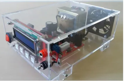
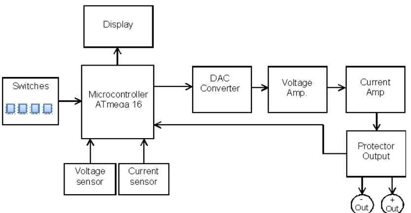
Assembly of this project is the digital power supply. The microcontroller used in the circuit is ATMEGA 16, a member of Atmel’s AVR microcontroller family. The main features of the power supply are the adjustable output voltage level and protection current limiter. Character 16x 2 of LCD is used as a control interface to set the parameters of voltage and current, and as displays for monitoring the actual values of voltage and current parameters that must be controlled. The output voltage of this device is 0-13 volts and the current is 1.5 amperes.
The Digital Power Supply Unit conforms to the following specifications:
Digital Power Supply Unit SPECIFICATIONS
NO CRITERIA REQUIREMENTS
1. Rated Input Voltage 220 VAC (+/-) 10%
3. Set Voltage Accuracy Set Voltage (+/-) 100mV
4. Output Voltage Ripple < 50mVAC
The Digital Power Supply Unit can be operated with the following controls:
FRONT PANEL CONTROL
SYM DESCRIPTION FUNCTION
SW1 SWITCH Turn ‘ON’ & ‘OFF’ Power Supply Unit
S2 MENU
Navigate continuously through the following modes:
S3 UP Increase Set Voltage
S4 DOWN Decrease Set Voltage
S5 OK Program Run / Function
JA +OUTPUT Power Supply DC Output Voltage (+)
JB -OUTPUT Power Supply DC Output Voltage (-)
Fig 2 : Block Diagram Assembly Project
3. INSTRUCTION TO THE COMPETITOR
Time limit is 4 hours.
Complete this Assembly Project using given materials and documents.
➢ Diagram list
➢ Schematic : Main PCB, Panel PCB
➢ Component Layout : Main PCB Top, Main PCB Bottom, Panel PCB
Top, Panel PCB Bottom ➢ Photographs for assembling ➢ Operating description
4. Parts list (BOM)
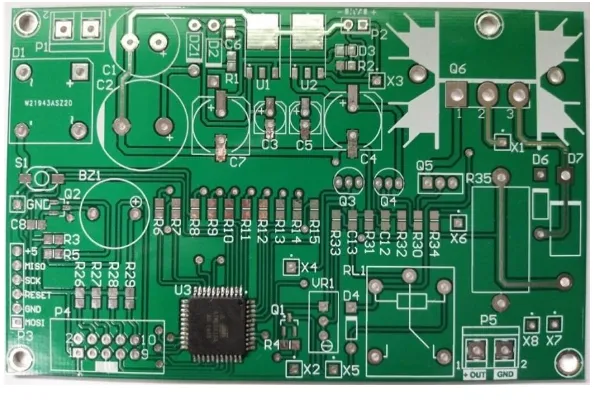
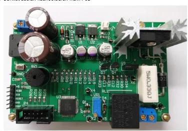
4.1. Main PCB
No. Qty Value Description Part Number
1 1 0.33 Resistor, 5W, 5% R35
2 1 470 Resistor SMD 0805 R2
3 1 1k Resistor SMD 0805 R5
4 1 1k8 Resistor SMD 0805 R31
5 3 4k7 Resistor SMD 0805 R1, R30, R32
6 1 5k6 Resistor SMD 0805 R34
7 15 10k Resistor SMD 0805
R3, R16, R17, R18, R19, R20, R21, R22, R23, R24, R33, R26, R27, R28, R29
8 12 20k Resistor SMD 0805
R4, R6, R7, R8, R9, R10, R11, R12, R13, R14, R15, R25
9 1 10K Multi turn variable
resistor VR1
10 2 22pF Capacitor SMD 0805 C10, C11,
11 5 100nF Capacitor SMD 0805 C6, C8, C9, C12, C13
12 2 22uF/35V Aluminium electrolytic
capacitors, 5× 5 dia C3, C5 13 2 330uF/25V Aluminium electrolytic
capacitors, 10× 10 dia C4, C7, 14 1 2200uF/25V Capacitor, Electrolytic,
2 mm pitch, 12 mm dia C1 15 1 4700uF/25V Capacitor, Electrolytic,
2 mm pitch, 16 mm dia C2
16 2 IN4001/
IN4002
Diode 1 A, footprint
DO-41 D2, D6
17 1 KBPC308 Bridge diode 3A, size
15.9x15.9 mm D1
18 1 1N5401
3A General Purpose Plastic Rectifier, footprint DO-201AD
D7
19 1 1N4148
1A General Purpose Plastic Rectifier, footprint DO-35
D4
20 1 8V2 Diode zener 1 watt DZ1
No. Qty Value Description Part Number
SOT23_N
23 1 BC547 Transistor NPN
footprint SOT54 Q3
24 1 BC557 Transistor PNP
footprint SOT54 Q4
25 1 DB139 Transistor NPN Q5
26 1 TIP35 Transistor NPN Q6
27 1 MC78M05
5 V 1A Step-Down Voltage Regulator, footprint 369A-03
U1
28 1 MC78M12
12 V 1A Step-Down Voltage Regulator, footprint 369A-03
U2
29 1 Atmega16A
- AU
Microcontrollers,
footprint 44A_N U3
30 1 11.059200
MHZ
SMD Crystal, Load Capacitance 10,0pF to 75.0pF
Y1
31 1 TMB12A05 Buzzer BZ1
32 1 B3F-1020 SMD Push button size
5 mm S1
33 1 Relay Relay 12 Volt, 5 pin,
SPDT, omron RL1
34 1
2x5pin Male Header With cover ST
10 Pin, male, Pin Header, 2.54 mm Pitch P4
35 1
1x6Pin male Header single ST, yellow
6 Pin, Male, Pin Header, 2.54 mm Pitch P3
36 2 T-block 2
pin
2-Pin Terminal Blok, 5
mm Pitch P1, P5
37 1 1x2 white
connector
MHDR 1x2, 2.54 mm
Pitch P2
4.2. Panel PCB
No Qty Value Description Part Number
1 1 270 Resistor SMD 0805 R36
2 1 5K Multi turn variable
resistor VR2
3 1 100nF Capacitor SMD 0805 C14
4 1 SN74HC59
5D
Register IC SMD,
footprint D016_N U4
5 4 B3F-4050
Tactile Switch size 12x12 mm, DC 24 V, 50 mA
SW1, SW2, SW3, SW4,
6 4 knob Tactile Switch square knob Switch
7 1
TG12864E-01XWBV
16x2 alphanumeric
LCD LCD1
8 1
2x5 pin
Male
Header With cover ST
10 Pin, male, Pin Header, 2.54 mm Pitch P6
9 3 Plug 1 pin Plug test point 1 pin X10, X11, X12
4.3. Power Supply Box
No Qty Value Description Part Number
1 1 AC Cord Cable
2 1 770W-X2/12
Inlet, 250V, 2.5A,
28x16 mm, Panel
Thickness + fuse
P7
3 1 SLE10A2
Rocker Switch,
125VAC, 10A, SPST, 20 mm dia
SW1
4 1
Step Down
Transformer,
110/220/230 primary, 0- 18V
T1
5 1 Fan DC 12 Volt,
60x60mm F1
6 1 Fan nets 60x60 mm
7 2 IDC socket S10 - A1 P4’, P6’
10 1 Heat sink for TIP35 35mmx12.5mm
11 1 1,5 M Wire, 18 AWG, Black
12 1 1,5 M Wire, 18 AWG, Red
13 1 20 cm layer cable, 10 layer
14 1 15 cm Shrinkable Tubing,
Black, 4mm dia
15 1 15 cm Shrinkable Tubing,
red, 4mm dia
16 8 Spacer, metal,
Hexagonal, M3x10 mm
17 7 Screw Pan Head,
metal M3x8mm
18 4
Screw, Pan Head, Brass, Nickel Plated, M3x35mm
19 2
Screw, Pan Head, Brass, Nickel Plated, M4x8 mm
20 6 Hexagonal Nut M3,
metal
21 2 Hexagonal Nut M4
22 10 Cable Ties, 2.5x100
mm
23 1 Acrylic Casing 19 x 14
5.
Proses AssemblyPastikan semua komponen lengkap
Fig 20 Semua komponen
5.1. Perakitan Main PCB
Merakit main PCB berdasarkan main PCB skematik dan main PCB list
komponen.
Spesifikasi ketinggian
(1) IC ATmega 16 sudah dipasang oleh panitia.
(2) Kapasitor, buzzer, transistor SMD SOT23, resistor DIP, Resistor SMD Diode, Led,
Socket, connector, Relay, T- block, Switch button, harus menempel pada
permukaan PCB.
(3) Transistors tipe TO 92 adalah 5mm – 7mm dari permukaan PCB.
(6) Berikut adalah hasil solderan main PCB
Fig 22 Main PCB Atas, Setelah Assembly
5.2. PANEL PCB ASSEMBLY
Perakitan PCB depan berdasarkan Panel PCB skematik dan Panel PCB list
komponen.
a. Assembly kapacitor, Resistor, IC, test point, variable resistor dan header 2 x5 pin
pada sisi bawah dari PCB.
Fig 24 Panel PCB Bawah
b. Assembly Push Button pada sisi atas dari PCB, diberi jarak +- 3mm dari PCB.
c. Gabungkan LCD dan PCB depan dengan 16 pin Header.
Fig 26 Gabungkan LCD dengan 16 pin header
Assemble LCD pada atas of PCB
Fig 27 Assembly LCD
5.3. Assembly dan pengkabelan instalasi power.
a. Assembly Inlet AC, Kipas, Jaring Kipas, Rocker Switch, Transformer, Soket Banana pada kotak acrylic.
Fig 29 Assembly asesoris
Fig 31 Assembly Transformer
Fig 32 Assembly Rocker Switch
Fig 34 Assembly kipas dan jarring kipas
b. Assembly dan pengkabelan instalasi power.
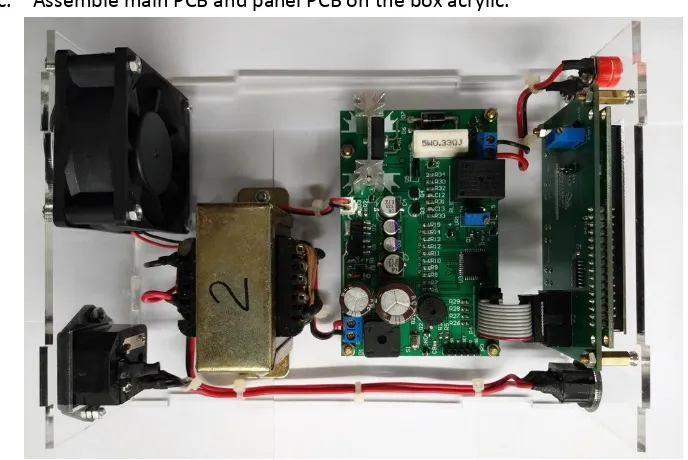
c. Assemble main PCB and panel PCB on the box acrylic.
Fig 36 Assembly main PCB dan panel PCB
Fig 37 Assembly main PCB
d. Wiring connection.
Pengkabelan sesuai dengan KKIN_NAS_VI_ASM _06_ID.pdf, Gambar instalasi.
Fig 39 Jalur pengkabelan
Fig 42 Pengkabelan transformer sekunder (0 – 18 V)
Fig 44 Pengkabelan soket banana
Fig 46 Panjang IDC socket
Fig 47 Panjang IDC socket
Fig 48 Panjang DC socket
Hasil Perakitan
Modul 3
FAULT FINDING, REPAIR AND
MEASUREMENT
Foto: Hadi Hardiansyah (Jawa Barat)
Test Project Document
LKS_2018_FFRM_EN
Submitted by:
Name
: Tim Elektronika LKS ASC WSC
Member
: ASC WSC Team ID
1. Description
Name of project is Frequency analyzer.
Figure 1. PCB “8 Band Audio Spectrum Analyzer”
This project is 8 Band Audio Spectrum Analyzer. A spectrum analyzer measures the magnitude of an input signal versus frequency within the full frequency range of the instrument. The primary use is to measure the power of the spectrum of known and unknown signals.
By analyzing the spectra of electrical signals, dominant frequency, power, distortion, harmonics, bandwidth, and other spectral components of a signal can be observed that are not easily detectable in time domain waveforms. These parameters are useful in the characterization of electronic devices, such as wireless transmitters.
Spectrum analysis can be used at audio frequencies to analyse the harmonics of an audio signal. A typical application is to measure the distortion of a nominally sine wave signal.
2. Block diagram
The block diagram is shown in Fig 2.
Figure 2. Block diagram for “ 8 Band Audio Spectrum Analyzer”
3. Recording of faults
Record the evidence of each fault using the attached sheets and symbols shown below.
FAULT
SYMBOL
DESCRIPTION FAULT
SYMBOL
DESCRIPTION
Open
(part, wire or PCB trace)
Stuck at high voltage (pin, input, output, etc.)
Short
(part, wire or PCB trace)
Stuck at low voltage (pin, input, output, etc.)
Part with larger value (resistor, capacitor,
etc.)
?
Incorrect part
number or wiring connecting
Part with smaller value
(resistor, capacitor, etc.)
+/-Wrong Polarity
Reference component locations accurately. Refer to examples shown below.
LOCATION CATEGORY SAMPLE
Power +5V / +12V / -5V / -12V / GND
Pin of IC IC2_8
Component of R/C/L R7_1(left/up:1 right/down:2)
Test Point TP1
Example
DEFECTIVE PART FAULT SYMBOL
Fault #1 IC2_8 - R7_1
BEFORE AFTER
Measurement #1
Node: R7_1___
DEFECTIVE PART FAULT SYMBOL
Fault #2 R1
BEFORE AFTER
Measurement #2
1.00V/DIV 1.00ms/DIV
Node: _TP1______
GND GND
2ms 4ms
5.00V 5.00V
Tegangan pada R7_ 1 dibawah 1V
4.
Recording of Measurement
Each measurement should show how to measure by using the symbol as below.
TOOLS SIMBOL
Power Supply
Voltmeter
Ammeter
Oscilloscope
Function Generator
GND
Example measuring schematic:
V
A
FG
CH1 CH2
GND Vcc
TP1 TP2
5.
Best Practice
to
Make jumper wire
4.1. Wire routing
Unless otherwise specified by high speed/high frequency requirements, route jumper wires the shortest route in straight legs as possible, avoiding test points, to points of termination. Allow enough length for routing, stripping and attachment.
Jumper wire routing on assemblies having the same part number should be the same pattern. Routing shall be documented for each part number and followed without deviation.
Do not allow jumper wires to pass over or under any component, however, they may pass over parts such as thermal mounting plates, brackets and components that are bonded to the PWB.
Jumpers may pass over solder lands if sufficient slack is provided so they can be moved away from the solder land for component replacement. Except for connectors at the edge of the board, do not pass jumpers through component foot prints unless the layout of the assembly prohibits the routing in other areas. Do not pass jumpers over patterns or vias used as a test point..
4.1.1. Target
➢ Wire routed shortest route.
➢ Wire does not pass over or under component.
➢ Wire does not pass over land patterns or vias used as points.
4.1.2. Defect
➢ Wire routed under or over components.
➢ Routing of wire(s) overhang or wrap over the edge of the board.
➢ The wire is loose and can extend above the height of adjacent components.
4.2. Supported Holes 4.2.1. Target :
➢ Wires soldered into a PTH/Via hole
4.2.2. Defect :
4.3. Wrapped Attachment 4.3.1. Target :
➢ Wire is wrapped a minimum of 90° on a flat lead or 180° on a round lead.
➢ Acceptable solder connection at wire/lead interface.
➢ Wire contour or end is discernible in the solder connection.
➢ Wire overhang of component termination does not violate minimum electrical clearance.
4.3.2. Defect :
➢ Wire is wrapped less than 90° on flat or less than 180° on round leads.
Answer Sheet
Competitor Name Table Number Signature
Fault-Answer Sheet
DEFECTIVE PART FAULT SYMBOL
Fault #1
BEFORE AFTER
Measurement #1
Node: _______
DEFECTIVE PART FAULT SYMBOL
Fault #2
BEFORE AFTER
Measurement #2
DEFECTIVE PART FAULT SYMBOL
Fault #3
BEFORE AFTER
Measurement #3
Node: _______
DEFECTIVE PART FAULT SYMBOL
Fault #4
BEFORE AFTER
Measurement #1
DEFECTIVE PART FAULT SYMBOL
Fault #5
BEFORE AFTER
Measurement #5
Node: _______
DEFECTIVE PART FAULT SYMBOL
Fault #
BEFORE AFTER
Measurement #
Verify graph output
Calculate the voltage using the formula
...
Calculate the frequency using the formula
#Info Tambahan
Silahkan download datasheet, schematic pdf, PCB dan video pada website:
Modul 4
SOFTWARE DESIGN
Test Project Document
LKS_2018_ESP_EN
Submitted by:
Name
: Tim Elektronika LKS ASC WSC
Member
: ASC WSC
Type
: Open hardware & Colse Firmware
1. Description
Hardware used is Line Follower V1.2 robot (LF V1.2). LF V1.2 is a small robot. LF V1.2 is a small robot with a size of 100 x 100 mm. Type of motor used is N20 with speed 1000Rpm at 12V. The main control of this robot is a microcontroller type ATmega16/32 and there is include a downloader type USBAsp on this robot, so that directly connected to the computer when the user is doing the programming. This robot can work with a voltage power of 6 to 12 Volts, but in competition later, this robot uses voltage 7.4V (LIPO 2S 850mA). Competitor have to program the Line Follower following instruction until can run normally in the track.
Figure 1. Line follower V1.1
2. Description of project and tasks
3. Software
All competitors are required to use Atmel studio 7. Template, libraries and tutorials will be uploaded on the website www.inaskills-electronics.com/lks2018. In the competition participants will be given a template by the jury.
4. Interface
This Line follower use interface: ➢ 6 light sensor (ADC) ➢ LCD Character 16x2 ➢ 4 push button
➢ 2 Motor with gearbox (PWM)
5. Schematic
5.2 Controller
5.3 Sensor
5.5 4 bit LCD 16x2
5.8 Pasive Buzzer
5.9 Downloader
6. Detail hardware
Sensor
Roda Ø34 mm
Roda Ø34 mm
Atmega 16/32
Downloader USB Asp
USB
Downloader Ball Caster
H=10mm
7. Track design competition F IN IS H S T A R T S T A R T 2 4 0 ,0 120,0 100 100 2 1 2 0 m m 10 2 0 2 6 m m 1 5 10 31 52 1 7 12 6 0 18
8. PCB Design
List Components.
Comment Designator Value Footprint Quantity
8-Bit AVR Microcontroller
U7 Atmega 8 32A_M 1
8-Bit AVR Microcontroller
U6 Atmega16 44A_M 1
Capacitor C11, C12, C20, C21 22pF C0805 4
Capacitor C5, C15, C18, C19, C22, C26, C27, C29, C33, C34
100nF C0805 10
Capacitor C4, C6, C7, C8, C13, C14, C30, C32
100nF C1206 8
Resistor C35, C36, C37, C38, C39, C40 2.2nF Chip_R0805 6
Polarized Capacitor (Surface Mount)
C1, C2, C3, C17, C9, C10 470uF CAPOL-X-7343-43 6
Polarized Capacitor (Surface Mount)
C28 220uF CAPOL-X-7343-43 1
Capasitor C16 1000uF capSMD10
Aluminium
1
Resistor R31, R33 150K Chip_R0805 2
Resistor R32, R34 100K Chip_R0805 2
Resistor R41 1.5K Chip_R0805 1
Resistor R42 680 Chip_R0805 1
Resistor R10 1K8 Chip_R0805 1
Resistor R1, R9 1K R0805 2
Resistor R11, R12 4K7 R0805 2
Resistor R2 8K2 R0805 1
Resistor R26, R27, R28, R29 680 R0805 4
Resistor R3, R16, R17, R20, R21, R25, R30
220 R0805 7
Resistor R4, R5 1K5 R0805 2
Resistor R6, R13, R18, R19, R22, R23 10K R0805 6
Resistor R7, R8, R14, R15, R24 68 R0805 5
Schottky Diode D2 SS36 DO214AC 1
Default Diode D5, D23, D24, D25, D26, D31, D32, D33, D34, D35
M7 DO214AC 10
Default Diode D1 1N5402 DO-201-15 1
Pole, Double-Throw Switch
S5 Switch 6pin ON OFF DPDT-6 1
Crystal Oscillator Y1 12MHz HC-49/SM 1
Crystal Oscillator Y2 16Mhz HC-49/SM 1
Header, 2-Pin P1 Header male 2x1 HDR1X2 1
Header, 3-Pin, Dual row
P2 Header male 3x2 HDR2X3_CEN 1
Magnetic Transducer Buzzer
LS1 Pasive buzzer SMD KLJ-9025 1
Inductor L1 47uH L-MS127 1
Liquid Crystal Display LCD1 LCD 16x2 neumaric LCD 1602 1
LED D10, D11 LED Blue LED0805 2
LED D19, D20, D27, D28 LED Green LED0805 4
Comment Designator Value Footprint Quantity
LED D4 LED Red LED_0805 1
USB 2.0, Right Angle, SMT, AB Type, Receptacle, 5 Position, Black
J1 Mini USB Mini USB AB -
440479
1
Motor, General Kind B1, B2 Motor DC 12V
1000Rpm
N20 Motor + Wheel 2
2
Dual Full Bridge Driver U9 L298P SO20_M 1
Sensor U0, U1, U2, U3, U4, U5 QRE1113g /
TCRT5000
Sensor LF 6
SMD Solder Jumper CB1, CB2, CB3 SJ 3
Switch S0, S1, S2, S3, S4 SMD 2 Pin SKQY_SMD Tact
Switch
5
Zener Diode D6, D7 3V3 SOD-80 2
Zener Diode D8, D9, D18 1N4148 SOD-80 3
Quad 2-Input NOR Buffered B series Gate, 14-Pin SOIC
U10 CD4001 SOIC14A_M 1
NPN Bipolar Transistor Q1, Q2 9013/3904 SOT23_M 2
Precision 500mA Regulator
U11 L78M05 TO-252 1
SIMPLE SWITCHER® 3A Step-Up Voltage Regulator
U8 LM2576-ADJ TS5B_M 1
Roda Pololu roda 34mm 2
Battry Lipo 2S 850mA 1
Charger Charger Lipo 2S 1
Ball caster Metal H10mm 1
Pcb PCB LF Inaskills Design 1
Hit sink 9x9mm 2
#Info Tambahan
Silahkan download\ template, tutorial, schematic pdf, dan video pada website:
INFORMASI PENTING
1. Baca dan pahami secara baik rule pedoman LKS.
2. Baca dan pahami secara baik Technical Description (TD) bidang Electronics.
3. Software yang digunakan dalam LKS 2018 sesuai dengan TD.
4. Peserta wajib membawa alat sesuai dengan yang tercantum pada TD, tolong selalu aktif dalam group/ email/ website ina skills terutama tujuh hari sebelum perlombaan untuk memastikan perubahan dari panitia tentang alat sesuai dengan kebijakan angaran dari direktorat.
5. Alat yang dibawa oleh peserta dari sekolah harap dibawa pada saat familiarisasi alat.
6. Peserta dibolehkan merubah tataletak alat dan pengkabelan pada work station/ meja kerja sesuai dengan kebutuhan peserta.
7. Software penunjang harus diinstal pada saat peserta masih berada didaerah/ tempat latihan, dikarenakan waktu familiarisasi yang singkat. Juri tidak bertanggung jawab jika pada saat lomba terjadi ketidak siapan software pada komputer peserta.
8. Peserta dan pembimbing masing masing harus membawa laptop. Laptop peserta akan ditinggal ditempat lomba saat familiarisasi hingga perlombaan selesai (tidak diperkenankan dibawa kepenginapan saat kompetisi). Untuk latihan di tempat penginapan peserta bisa menggunakan laptop pembimbing. Catatan: untuk laptop peserta disaranan disk dalam kondisi kosong atau tidak ada data yang penting.
9. Selalu aktif untuk membuka website www.inaskills-electronics.com untuk mendapatkan tutorial tutorial dan informasi tambahan penting dalam persiapan LKS 2018.
11. Saat perlombaan berlangsung tidak ada buku atau kertas diatas meja dan semua tas harus dimasukan dalam loker yang telah disediakan oleh panitia.
12. Utamakan keselamatan dan kesehatan kerja. sarung tangan akan disediakan oleh panitia.
13. Jika peserta terdapat melakukan kecurangan dengan bukti yang jelas maka akan dikenakan pengurangan nilai atau diskualifikasi.
14. Persiapan LKS yang sangat singkat, tolong manfaatkan waktu sebaik baiknya, perkuat dasar/ basic.
15. Jadwal istirahat peserta menyesuaikan waktu ibadah setempat. Bagi Muslim harap untuk membawa sendal jepit dan sajadah serta mukena bagi perempuan.
SELAMAT BERLATIH !!!
Soal akan berubah minimal 30%
Mungkin ada informasi tambahan mengenai persiapan LKS NASIONAL 2018, Mohon selalu membuka web inaskills
www.inaskills-electronics.com/lks2018
Forum group WA silahkan hub email: [email protected]
Dengan format pesan
Asal Sekolah :
Provinsi :
Nama Pembimbing :
TTL Pembimbing :
No Handphone Pembimbing :
Nama Peserta :
TTL Peserta :