ABSTRACT
DESIGN, FABRICATION AND CHARACTERISATION OF FREE-STANDING THICK-FILM PIEZOELECTRIC CANTILEVERS FOR ENERGY
HARVESTING
by Swee-Leong, Kok
ii
Contents ...ii
List of Figures ... vi
List of Tables ... xiii
Acknowledgements ... xiv
Nomenclature ... xv
Abbreviations ... xvii
Chapter 1 Introduction ... 1
1.1 Overview of The Technology ... 1
1.2 The Scope of the Book ... 3
1.3 The Book Structure ... 4
Chapter 2 Literature Review ... 6
2.1 Introduction ... 6
2.2 Piezoelectricity ... 7
2.2.1 Constituent Equations of Piezoelectricity ... 8
2.2.2 Piezoelectric Material Measurement Methods ... 10
2.2.3 Piezoelectric Materials... 13
2.2.4 Lead Zirconate Titanate (PZT) ... 14
2.3 Piezoelectric Applications ... 15
2.4 Vibration Energy Harvesting ... 17
2.4.1 Generic Mechanical-to-Electrical Conversion Model ... 18
2.4.2 Analytical Model of Piezoelectric Harvester ... 20
2.4.3 Cantilever-Based Piezoelectric Energy Harvesters ... 22
2.4.4 Performance Comparison ... 26
2.5 Thick-Film Technology ... 29
2.5.1 Evolution of Thick-Film Technology ... 29
2.5.2 Standard Fabrication Process ... 30
2.6 Thick-Film Free-Standing Structures ... 32
2.6.3 Thick-Film Sacrificial Layer Techniques ... 38
2.7 Conclusion ... 40
Chapter 3 Free-Standing Cantilever Structure Designs ... 41
3.1 Introduction ... 41
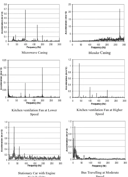
3.2 Ambient Vibration Sources ... 42
3.3 The Design Considerations ... 45
3.4 Theoretical Analysis of Multilayer Structures ... 46
3.4.1 Natural Frequency of a Unimorph Cantilever ... 47
3.4.2 Location of Neutral Axis of a Unimorph Cantilever ... 50
3.4.3 Maximum Allowed Stress ... 51
3.4.4 Maximum Allowed Deflection ... 54
3.4.5 Estimated Output Voltage ... 55
3.5 Analysis and Discussion on Calculation Results ... 56
3.6 Computational Analysis ... 68
3.6.1 Modal Analysis ... 71
3.6.2 Comparison with Calculation Results ... 77
3.7 Screen Printing Design ... 80
3.8 Conclusion ... 82
Chapter 4 Processing of Thick-Film Free-Standing Devices ... 83
4.1 Introduction ... 83
4.2 Fabrication Materials ... 84
4.2.1 Lead Zirconate Titanate (PZT) Pastes ... 84
4.2.2 Carbon Pastes ... 85
4.2.3 Electrode Pastes ... 86
4.2.4 Substrate Materials ... 88
4.3 Thick-Film Printing Process ... 88
4.4 Three-Dimensional Co-Firing Technique ... 89
4.5 Co-firing Process... 91
4.6 Experiment Results and Discussion ... 92
4.6.1 Effect of PZT-Ag/Pd Fabrication Sequence ... 92
4.6.2 Effect of Air-Flow and Co-Firing Profile ... 95
4.7 Final Fabricated Samples and Polarisation ... 102
4.8 Conclusion ... 106
Chapter 5 Piezoelectric Materials Characterisations ... 107
5.1 Introduction ... 107
5.2 Thick-Film Dimensions Measurement... 108
5.3 Thick-Film Free-Standing Samples under SEM Inspection ... 111
5.4 Resonant Measurement ... 113
5.5 Direct Measurement (Berlincourt Method) ... 120
5.5.1 Effect of Substrate Clamping ... 120
5.5.2 Decay of d33 over Time ... 122
5.5.3 Comparison between Clamped and Unclamped Samples ... 126
5.6 Conclusion ... 127
Chapter 6 Testing under Harmonic Base Excitation ... 128
6.1 Introduction ... 128
6.2 Mechanical Properties of Cantilever Structure ... 130
6.3 Experimental Procedure ... 132
6.4 Mechanical Characterisation... 134
6.4.1 Excitation without Proof Mass ... 134
6.4.2 Excitation with Proof Mass ... 136
6.5 Electrical Characterisation ... 137
6.5.1 Excitation without Proof Mass ... 138
6.5.2 Excitation with Proof Mass ... 141
6.5.3 Comparison between Samples with Different Distance from Neutral Axis ... 143
6.5.4 Interdigitated Cantilever ... 145
6.6 Energy Conversion Efficiency ... 148
6.7 Conclusion ... 151
Chapter 7 Multimorph Cantilevers ... 152
7.1 Introduction ... 152
7.2 The Functioning Principle ... 153
7.3 Experimental Samples ... 158
7.4 Evaluation of Maximum Allowed Excitation with Proof Mass ... 160
7.5.2 Parallel polarised multimorph ... 168
7.5.3 Excitation with Proof Mass ... 173
7.6 Conclusion ... 176
Chapter 8 Multi-Frequency Piezoelectric Energy Harvesters ... 177
8.1 Introduction ... 177
8.2 The Functioning Principle ... 179
8.3 Multi-Cantilever Design ... 181
8.4 ANSYSTM Simulation Results and Discussion ... 184
8.5 Experimental Results and Discussions ... 189
8.5.1 Excitation without Proof Mass ... 192
8.5.2 Excitation with Proof Mass ... 198
8.6 Conclusion ... 200
Appendix A ...201
Appendix B ...202
Appendix C ...206
Appendix D ...214
vi
Figure 2-1: Schematic diagram of the electrical domain: (a) before polarisation, (b) during polarisation and (c) after polarisation. ... 7 Figure 2-2: Notation of piezoelectric axes. ... 9 Figure 2-3: Cross-sectional view of piezoelectric configuration mode, (a) d31 and (b) d33.
... 9 Figure 2-4: Impedance of a piezoelectric ceramic at resonance. ... 11 Figure 2-5: A schematic diagram of a spring-mass-damper system of a piezoelectric
FSD, based on the model developed by Williams et al [44]. ... 18 Figure 2-6: A diagram of an analogous circuit for a piezoelectric vibrated device with a
resistive load. ... 20 Figure 2-7: Design of prototype generator (after [5]). ... 24 Figure 2-8: (a) A rectangular cantilever microgenerator prototype (b) An improved
version (after [12]). ... 25 Figure 2-9: MEMS micromachined IDE pattern cantilever (after [15]). ... 25 Figure 2-10: Schematic structure of the vibration energy harvester based on air-spaced
piezoelectric cantilevers (after [50]). ... 25 Figure 2-11: Cantilever configuration of a MFC plate (a), a PZT plate (b) and a Quick
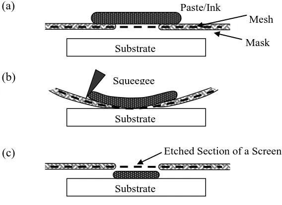
Pack actuator (c) (after [49]). ... 26 Figure 2-12: Thick-film screen printing steps. ... 31 Figure 2-13: A few examples of free-standing micromechanical structure [83]: (a)
cantilever, (b) bridge, (c) tunnel, (d) honeycomb, and (e) dome. ... 33 Figure 2-14: Micromachining process for fabricating a cantilever structure [26]. ... 35 Figure 2-15: Fabrication steps of surface micromachining based on sacrificial layer
technique [14]. ... 36 Figure 2-16: Fabrication steps for a ‘flip-and-bond’ technique [87]. ... 37 Figure 2-17: Piezoelectric polyimide free-standing structure fabrication steps [27]. ... 38 Figure 2-18: Fabrication steps for thick-film sacrificial layer technique. ... 39 Figure 3-1: Typical low level ambient vibration sources. ... 43 Figure 3-2: A cross-sectional view of a unimorph structure. ... 48 Figure 3-3: (a) Side view of Bending beam with bending moment and radius of
curvature, (b)Transformed cross-section of a composite unimorph beam, with PZT layer width, wp and transformed electrode width of nepwp. ... 50
Figure 3-4: Bending beam of unimorph structure. ... 51 Figure 3-5: Parallel-axis for a transformed cross-section of a unimorph. ... 52 Figure 3-6: Diagram of a multimorph cantilever structure. The theoretical model was
based on a unimorph sandwiched structure of PZT, lower and upper electrodes. 56 Figure 3-7: Experimental data of mechanical damping ratio as a function of cantilever
length (a) and proof mass (b). The dotted lines are a fitting line to illustrate that the mechanical damping ratio is proportional to the cantilever and proof mass. ... 57 Figure 3-8: Experiment data of optimum resistive load as a function of cantilever length
(a) and proof mass (b). The dotted lines illustrate the change of optimum resistive load at resonant frequency. ... 58 Figure 3-9: Experimental data of structural coupling factor as a function of cantilever
Figure 3-10: Theoretical calculation of cantilever length variation effect on maximum stress (a) and maximum deflection for two cases (b); one with damping fixed at 0.0037 and the other one is the value measured from experiment as shown in Figure 3-7 (a). ... 59 Figure 3-11: Theoretical calculation of the cantilever length variation effect on output
power at a constant resistive load of 20 kΩ. ... 60 Figure 3-12: Theoretical calculation of the output power as a function of cantilever
length when driving resistive loads; at optimum resistive load and constant
resistive load at 20 kΩ. ... 61 Figure 3-13: Theoretical calculation of the lower electrode thickness variation effect on
maximum stress (a) and maximum deflection (b) on two conditions; one with constant upper electrode he2 at 15 µm (condition-A) and another one with constant
total thickness at 116 µm (condition-B). ... 62 Figure 3-14: Theoretical calculation of the condition-A (constant upper electrode) and –
B (constant total thickness) effect on output voltage (a) and output power (b). ... 63 Figure 3-15: Theoretical calculation of the PZT thickness variation effect on maximum
stress induced on the structure at a constant base excitation. ... 63 Figure 3-16: Theoretical calculation of the PZT thickness variation effect on output
power. ... 64 Figure 3-17: Theoretical calculation of the base input acceleration effect on maximum
deflection for a cantilever with length 18 mm. ... 64 Figure 3-18: Theoretical calculation of the base input acceleration effect on output
voltage (a) and output power (b) for a cantilever with length 18 mm at resonance. ... 65 Figure 3-19: Theoretical calculation of the maximum deflection as a function of proof
mass at an acceleration of 10 m/s2 for two different cases; the dotted line is calculated with a fixed damping ratio at 0.0037 and the solid line is calculated base upon the experimental damping value according to Figure 3-7 (b). ... 66 Figure 3-20: Theoretical calculation of the proof mass variation effect on output voltage
(a) and output power for two scenarios (b): (1) Fixed values of damping at 0.0037 and coupling factor 0.06 and (2) Experimental values of damping and coupling factor. ... 67 Figure 3-21: Theoretical calculation of the electrical output voltage (a) and output
power (b) as a function of electrical resistive load for three different damping factors. ... 67 Figure 3-22: A schematic diagram of a unimorph cantilever (a) and a cantilever with
mesh on used for simulation in ANSYS (b). ... 68 Figure 3-23: Diagram of multilayer cantilever structure. ... 69 Figure 3-24: Contour plot of stress distribution of a cantilever with dimension as shown
in Table 3-3 under fundamental (a), 2nd order (b), 3rd order (c) and 4th order (d) vibration modes. ... 73 Figure 3-25: Diagram of maximum stress as a function of base excitation frequency for
a cantilever having the dimension as shown in Table 3-3 ... 73 Figure 3-26: Contour plot of stress distribution of a cantilever beam having a width of
18 mm under fundamental (a), 2nd order (b), 3rd order (c) and 4th order (d) vibration modes. ... 74 Figure 3-27: Diagram of maximum stress as a function of base excitation frequency for
a cantilever having a width of 18 mm. ... 74 Figure 3-28: Cantilever with full-width-coverage tungsten proof mass; contour plot of
Figure 3-29: Diagram of maximum stress as a function of base excitation frequency for a cantilever attached with full-width-coverage proof mass. ... 75 Figure 3-30: Contour plot of stress distribution of a cantilever beam attached with
full-width-coverage proof mass for fundamental (a), 2nd order (b), 3rd order (c) and 4th order (d) vibration modes. ... 76 Figure 3-31: Diagram of maximum stress as a function of base excitation frequency for
a cantilever attached with full-width-coverage proof mass. ... 76 Figure 3-32: Comparison between ANSYS simulations and theoretical calculation
results on its natural frequency (a), maximum cantilever tip acceleration (b), maximum stress (c) and maximum deformation on the tip of the cantilever (d). . 79 Figure 3-33: A free-standing cantilever structure design layout. ... 80 Figure 3-34: Layouts of a plated electrode (a) and an IDE cantilever structure (b). ... 81 Figure 4-1: Thermogravimetric analysis (TGA) of graphite heated in air at 10 °C/min
[100]... 86 Figure 4-2: A photograph of Ag/Pd films printed on carbon sacrificial layers. ... 89 Figure 4-3: Three different co-firing profiles for fabricating free-standing structure. .. 91 Figure 4-4: Photographs of failed free-standing structure comprising only (a) PZT and
(b) Ag/pd materials. ... 93 Figure 4-5: Composite structures of Ag/Pd conductors and PZT ceramics printed in
sequence and co-fired together: (a) ceramic (A-P), (b) conductor-ceramic-conductor (A-P-A), (c) conductor-ceramic- conductor-ceramic (A-P-A-P) and (d) conductor-ceramic-conductor-ceramic-conductor (A-P-A-P-A). ... 94 Figure 4-6: (a) Composite structures of PZT ceramics as the lower layer followed by
printed Ag/Pd conductors and co-fired together, (b) Composite of ceramic-conductor-ceramic-conductor. ... 95 Figure 4-7: A photograph of failure free-standing structure fabricated with reduced air
flow. ... 96 Figure 4-8: Thick-film co-fired with 550 Profile. ... 96 Figure 4-9: Thick-film co-fired with: (a) 850 and (b) 950 Profile. ... 97 Figure 4-10: Schematic diagram of an arrangement of alumina substrates with a gap of 2
mm. ... 97 Figure 4-11: IDT patterned electrode on ceramic-conductor composite structure: (a)
schematic diagram of a conductive layer printed on seven layers of ceramic; (b) fabrication results. ... 98 Figure 4-12: Enhanced structures with a layer of ceramic printed over Ag/Pd IDT
conductors. ... 99 Figure 4-13: A layer of Ag/Pd as supporting layer can prevent the cermet from cracking
after co-firing. ... 99 Figure 4-14: Upper and lower electrodes peeling off from ceramic layers. ... 100 Figure 4-15: Composite films of ceramic-electrode-ceramic-electrode which curve
side-way and pull off from substrate. ... 101 Figure 4-16: Flatter free-standing structures as a result of protective films of ceramic
printed on both upper and lower side of the structures. ... 101 Figure 4-17: Photograph of fabricated samples of free-standing cantilever with different
lengths with a gap height of 2 mm. ... 102 Figure 4-18: Photographs of free-standing structures: a) original designed model, with
length, l0 and width, w0; b) samples of fabrication outcome. ... 103
Figure 4-19: Sample A1 with no additional PZT covers on the upper electrode. ... 103 Figure 4-20: Polarisation set-up. ... 104 Figure 5-1: Photographs show: (a) A SPIDA system set-up and (b) a thick-film sample
Figure 5-2: PZT thickness before and after co-firing. ... 111 Figure 5-3: SEM micrographs of samples co-fired at 850 °C and 950 °C under
magnification of ×300, ×800 and ×4000. ... 112 Figure 5-4: Comparison of sample D and C series for the value of capacitance over the
ratio of area/thickness (with ± 5% error). ... 114 Figure 5-5: Frequency response for sample D1, D2, D3, D4 and D5, corresponds to their
impedance. ... 115 Figure 5-6: Frequency response for sample C series. ... 116 Figure 5-7: Resonant frequency as a function of inverse of cantilever length. ... 117 Figure 5-8: Coupling factor of sample D and C series as a factor of material length. 117 Figure 5-9: The impedance at resonance is proportional to the ratio of thickness to the
area of the material. ... 118 Figure 5-10: Mechanical quality factor, Qm for sample C and D series. ... 119
Figure 5-11: A photograph (a) and a schematic diagram (b) showing a piezoelectric specimen being measured with the Berlincourt measurement method. ... 120 Figure 5-12: Diagram of a free-standing film in expansion (a) and contraction (b)
compared to a clamped film in expansion (c) and contraction (d). ... 121 Figure 5-13: Photographs of (a) a clamped sample printed across a score line on a
substrate and (b) an unclamped sample held with a pair of tweezers. ... 123 Figure 5-14: d33 as a function of time elapsed over 15 minutes for measurements taken
just after polarisation and six months after polarisation for a clamped sample. . 123 Figure 5-15: d33 as a function of time elapsed for an unclamped sample just after
polarisation and six months after polarisation. ... 124 Figure 5-16: The d33 value as a function of time elapsed for free-standing samples
co-fired at 850 °C and 950 °C. ... 125 Figure 5-17: Comparison of d33 value between unclamped (free-standing) samples and
clamped sample. ... 126 Figure 6-1: Diagram of a free-standing unimorph cantilever structure. ... 128 Figure 6-2: Free-standing cantilever samples; (a) photograph and (b) the dimensions of
a sample. ... 129 Figure 6-3: (a) Diagram of a sequence test system and (b) a shaker table where the
device is being tested. ... 133 Figure 6-4: Schematic diagram of four different proof masses M1 – M4 (shaded) with
the same thickness of 1 mm distributed on the tip of a cantilever. ... 133 Figure 6-5: Experimental results in agreement with theoretical calculation for resonant
frequency as a function of cantilever length. ... 134 Figure 6-6: QT as a function of cantilever length. ... 135
Figure 6-7: Experimental results in agreement with theoretical calculation for resonant frequency as a function of mass for sample D5 with length 13.5 mm. ... 136 Figure 6-8: QT as a function of mass for sample D5 for four different proof mass
distributions. ... 137 Figure 6-9: Coupling factor as a function of mass attached to a cantilever with length 18
mm. ... 137 Figure 6-10: Output power at resonant frequency as a function of electrical resistive
load when accelerated at a level of 100 milli ‘g’. ... 139 Figure 6-11: Optimum resistive load, Ropt as a function of cantilever length. ... 139
Figure 6-12: Output power at optimum resistive load as a function of cantilever length when excited to their resonant frequency at an acceleration of 0.1 ‘g’. ... 140 Figure 6-13: Output power as a function of excited frequency at different levels of
acceleration for sample D6, where 1 ‘g’ = 10 m/s2
Figure 6-14: Optimum resistive load, Ropt as a function of mass for sample D5 with
different configurations of proof mass as shown in Figure 6-4. ... 142 Figure 6-15: Output power at optimum resistive load as a function of mass for sample
D5 loaded with different distributions of proof masses. (Dotted lines show general trend). ... 142 Figure 6-16: Frequency response for sample A1, D5 and C3. ... 143 Figure 6-17: Output power as a function of resistive load for samples A1, D5 and C3.
... 144 Figure 6-18: Photograph of an IDE sample. ... 145 Figure 6-19: Output power of sample IDa1 as a function of resistive load at an
acceleration of 0.05 g and 0.5 g. ... 146 Figure 6-20: Frequency response comparison for sample D3, C2 and IDa1 at an
acceleration of 0.1 g and with resistive load of 30 kΩ. ... 147 Figure 6-21: Comparison of output power and natural frequency for sample D3, C2 and
IDa1 at 0.05 g. ... 147 Figure 6-22: Coupling coefficient as a function of optimum resistive load for different
damping ratio for sample D5, with resonant frequency at 505.5 Hz and capacitance of 6.82 nF. ... 149 Figure 6-23: Efficiency of energy conversion as a function of coupling coefficient and
Q-factor. ... 149 Figure 6-24: The energy conversion efficiency (equation (6-10)) as a function of
cantilever length (with 5 % error). ... 150 Figure 6-25: The energy conversion efficiency as a function of mass for sample D5. 150 Figure 7-1: Diagram of a side-view of a multimorph cantilever. ... 153 Figure 7-2: A diagram showing (a) downward and (b) upward bending position of a
series polarised multimorph cantilever, which produces an alternating output voltage at the output terminal. ... 153 Figure 7-3: Schematic diagram of (a) a multimorph structure and (b) transformed
cross-section of a composite multimorph structure. ... 154 Figure 7-4: Cross-sectional view of a composite multimorph with uniform thickness of
PZT and electrode layers. ... 156 Figure 7-5: Schematic diagram of a cross-sectional view of a composite multimorph
structure. ... 158 Figure 7-6: Polarisation mode: (a) Series and (b) parallel. The number beside each layer
denotes the fabrication sequence of electrode layers. ... 159 Figure 7-7: Schematic diagram of charges generation when the multimorph structures
were in upward bending position for a (a) series and (b) parallel polarised device. ... 159 Figure 7-8: Output power as a function of excited frequency at different acceleration
levels for sample BA1 (note that output power is displayed on a logarithmic scale). ... 160 Figure 7-9: Output power as a function of resistive load for upper section and lower
section of PZTs for a multimorph structure. ... 163 Figure 7-10: Output power as a function of resistive load for a multimorph cantilever
with a few different electrode configurations. ... 164 Figure 7-11: Output current-voltage for a series polarised sample. ... 165 Figure 7-12: Open circuit voltage as a function of acceleration level for a multimorph
cantilever with a few different electrode configurations. ... 166 Figure 7-13: Output power as a function of resistive load for a parallel polarised sample.
Figure 7-15: Open circuit voltage as a function of acceleration level of a parallel polarised sample. ... 171 Figure 7-16: Comparison of output power between excitation with and without proof
mass for the same multimorph sample (at connection 1;4 short 2+3). ... 174 Figure 7-17: Output power as a function of resistive load for the multimorph sample
when excited with and without proof mass. ... 174 Figure 7-18: Open circuit voltage as a function of acceleration level for the multimorph
cantilever sample. ... 175 Figure 7-19: Resonant frequency as a function of acceleration level for the multimorph
cantilever sample. ... 175 Figure 8-1: Comparison of simulated power output between individual cantilevers and a
multi-cantilever system consisting of 40 individual cantilevers at a vibration amplitude of 1 µm [118]. ... 180 Figure 8-2: A multi-cantilever with different cantilever lengths. ... 182 Figure 8-3: An array of cantilevers with three free-standing structures of different
length. ... 182 Figure 8-4: Multi-cantilever with an array of free-standing structures of different width.
... 183 Figure 8-5: ANSYSTM simulation results showing stress distribution on multi-cantilever
structures; (a) model with six fingers with different lengths, (b) cantilevers with masses attached on each finger, (c) model with three fingers with different lengths and (d) model with five fingers of different cantilever width. ... 184 Figure 8-6: Average stress of cantilever structure as a function of excited frequency for
multi-cantilever and individual cantilever with different lengths. ... 186 Figure 8-7: Average stress as a function of excited frequency for multi-cantilever
attached with proof mass. ... 187 Figure 8-8: Average stress as a function of excited frequency for multi-cantilever
attached with a combination of proof masses. ... 187 Figure 8-9: Maximum stress induced on the anchor of a cantilever structure as a
function of excited resonant frequency for multi-cantilever with 3 and 6 array of individual cantilevers. ... 188 Figure 8-10: Maximum stress as a function of excited resonant frequency for
multi-cantilever of five fingers with different widths, three fingers and six fingers. Insert: comparison of frequency response for multi-cantilever with different widths and those with different lengths. ... 188 Figure 8-11: A photograph of a multi-cantilever sample of (a) six fingers with different
lengths and (b) five fingers with different widths. ... 189 Figure 8-12: Schematic diagram showing the side view of (a) a composite
multi-cantilever structure and (b) polarisation arrangement. he1, he2, hp, hup and hlo
denotes the thickness of lower electrode, upper electrode, active PZT, upper non-active PZT and lower non-non-active PZT. ... 190 Figure 8-13: Photograph of a multi-cantilever attached with tungsten proof mass, M3.
... 190 Figure 8-14: Resonant frequency as a function of cantilever length and number of PZT
layers for a multi-cantilever structure. ... 192 Figure 8-15: Open circuit voltage as a function of excited frequency for a
multi-cantilever with reducing number of fingers from the shortest to the longest, when excited at 0.5 g. ... 193 Figure 8-16: Output voltage (at a resistive load of 20 kΩ) as a function of excited
Figure 8-17: Optimum resistive load as a function of cantilever length of a series of multi-cantilever with different number of cantilevers (fingers). ... 195 Figure 8-18: Log magnitude of output power as a function of driving frequency at
different levels of acceleration. ... 196 Figure 8-19: Lower and upper band of operation frequencies for an output power of 50
nW with varying cantilever lengths. The measurements were taken at excitation acceleration levels of 1 g and 0.5 g when driving a resistive load of 20 kΩ. ... 197 Figure 8-20: Output voltage as a function of excited frequency at resistive load of 5 kΩ
and 9 MΩ for a multi-cantilever with different width fingers. ... 198 Figure 8-21: Output power of multi-cantilever with each cantilever attached with
tungsten proof mass of 0.19 g (M1) when driving resistive load of 20 k at a range of driving frequencies. ... 199 Figure 8-22: Output power for various driving frequencies with a resistive load of 20
List of Tables
Table 2-1: Comparison of a few key experimental energy harvesters. ... 28
Table 3-1: Summaries of Measured Vibration Sources... 44
Table 3-2: Standard dimensions of a cantilever used to verify theoretical model. ... 56
Table 3-3: Initial parameter for ANSYS simulation. ... 70
Table 4-1: Comparison of material properties for silver, palladium and gold [94]. ... 87
Table 4-2: Summary of Polarised Samples. ... 105
Table 5-1: Thick-film thickness measured with SPIDA system. ... 110
Table 5-2: Summary of measurement results from resonant measurement method for sample C and D series. ... 119
Table 5-3: Parameters for 96 % alumina substrate [82]. ... 122
Table 5-4: Summary of measurement results for fabricated samples at standard 850 °C and 950 °C in comparison with bulk PZT from Morgan Electroceramics Ltd. .. 125
Table 6-1: Dimensions (in mm) of samples shown in Figure 6.2. ... 129
Table 7-1: Fabricated sample dimensions. ... 158
Table 7-2: Measurement of capacitance of all the possible configurations of terminal connection for series and parallel polarised samples. ... 162
Table 7-3: Summary of connection configurations for a series polarised sample. ... 167
Table 7-4: Summary of connection configurations for a parallel polarised sample. ... 171
Table 8-1: Simulation parameters. ... 181
Table 8-2: Summary of dimensions for a multi-cantilever with six fingers of different length. ... 182
Table 8-3: Summary of dimensions for a multi-cantilever with three fingers of different length. ... 183
Table 8-4: Summary of dimensions for a multi-cantilever with five fingers of different width. ... 183
Table 8-5: Dimensions of a fabricated multi-cantilever of six fingers with different lengths. ... 191
Acknowledgements
First and foremost, I would like to thank my PhD supervisor, Prof. Neil White for his ideas and guidance throughout my project. Thanks also go to my co-supervisor, Dr. Nick Harris for his helpful comments in my work.
My sincere gratitude also goes to Dr. Andy Cranny and Dr. Darryl Cotton for showing me the thick-film processing techniques. I appreciate Dr. Steve Beeby and Dr. Russel Torah for allowing me to use the shaker for characterising the samples. I am also thankful to Prof. Alun Vaughan and Prof. Michael Kraft for their comments and suggestions.
I am indebted to Prof. Martyn Hill and Dr. John Atkinson for their generosity in giving me a temporary office space to work in and granting me access to thick-film facilities in the Faraday Building after the fire incident at the clean room and Mountbatten building in Nov. 2005.
I also gratefully like to acknowledge the financial support from Universiti Teknikal Malaysia Melaka for the scholarship award to pursue this PhD. I would also like to thank School of Electronics and Computer Science for the fire extensions funding towards the end of the candidature.
Besides that, I would like to take this opportunity to thank my fellow colleagues and friends, Dr. John Tudor, Dr. Peter Glynne-Jones, Somphop Rodamporn, Dr. Dibin Zhu, Ivo Ayala, Dr. Elena Koukharenko, Ghaithaa Manla, Dr. Siti Ahmad, Noreha Abdul Malik, Dr. Neil Grabham, Alex Weddell, Dr. Geoff Merrett, Dr. Andrew Frood, Pedro Barbosa, Adam Lewis and many others in Electronic Systems and Devices Group, who have either been involved directly or indirectly in my project and particular making the lab a friendly and enjoyable place to work in.
Symbol Unit Description
F/m permittivity at constant stress F/m permittivity of vacuum
F/m permittivity of a piezoelectric material
kg/s2 spring constant of a spring-mass-damping system kg/m3 total density
kg/m3 density of electrode kg/m3 density of PZT
N/m2 stress dimensionless strain
ζ dimensionless damping ratio
ζe dimensionless electrical damping ratio
ζm dimensionless mechanical damping ratio
ζT dimensionless total damping ratio
dimensionless coefficient related to boundary conditions dimensionless Poisson’s ratio at constant or zero electric field
Hz driving angular frequency Hz angular natural frequency Hz angular resonant frequency m2 area of piezoelectric material
m2 base acceleration level
b kg/s generic damping factor
kg/s electrical damping for a spring-mass-damping system
kg/s mechanical damping for a spring-mass-damping system
F capacitance of a piezoelectric material F capacitance of a piezoelectric material C/m2 charge density
N/m bending modulus per unit width
m distance from neutral axis to the centroid of piezoelectric layer
C/N piezoelectric charge constant at stress applied direction i-polarisation and j
-N/C electric field
N/m elastic modulus for electrode layer N/m elastic modulus for piezoelectric layer
N/m total elastic modulus for a composite structure Hz antiresonant frequency of a piezoelectric ceramic Hz resonant frequency of a piezoelectric ceramic
Vm/N piezoelectric voltage coefficient at i-polarisation and j-stress applied direction
m electrode thickness m piezoelectric thickness
dimensionless coupling factor of piezoelectric cantilever
dimensionless relative dielectric constant at constant stress dimensionless coupling factor of piezoelectric material
m free-standing length m total beam length
kg lump mass of a spring-mass-damping system
kg proof mass
kg total cantilever mass
kg effective mass at the tip of a cantilever
P W output power in rms value
dimensionless Q-factor of a piezoelectric material dimensionless Q-factor of a cantilever structure
Ω resistive load
r dimensionless ratio of driving frequency to natural frequency m2/N elastic compliance at constant electric field
m2/N
elastic compliance at constant displacement (i =1 along its length; i = 3 along its thickness)
m2/N
elastic constant at constant electric field along its length
Tc °C Curie Temperature
V V output voltage in rms value
Y m amplitude base excitation
m base displacement of a spring-mass-damping system (t) m/s2 base velocity of a spring-mass-damping system (t) m/s2 base acceleration of a spring-mass-damping system m relative displacement of a spring-mass-damping
system
m/s velocity of a spring-mass-damping system m/s2 acceleration of a spring-mass-damping system
Abbreviations
µTAS Micro Total Analysis Systems
CVD Chemical Vapour Deposition
FoMV Figure of Merit for performance comparison of energy harvesters
IDE Interdigitated Electrode
IDT Interdigitated
MEMS Micro-Electro-Mechanical System
NPD Normalised Power Density
PVDF Poly(vinylidene Fluoride)
PZT Lead Zirconate Titanate
RF Radio Frequency
SEM Scanning Electron Microscope
SFM Scanning Force Microscopy
SPIDA Solder Paste Inspection Data Analyst
xviii
“We should be taught not to wait for inspiration to start a thing. Action always
generates inspiration. Inspiration seldom generates action”
1
Chapter 1
Introduction
1.1
Overview of The Technology
With the advancement in the areas of wireless technology and low-power electronics, a pervasive system [1] is made possible. This system is referred to a world where computational devices are embedded in the environment for intelligent buildings and home automation [2], autonomous vehicles [3] and also possible to be implanted in human bodies such as the one in body sensor networks for health monitoring [4]. To develop a totally autonomous system, however, traditional batteries, with limited life-span have to be replaced with energy harvesters, which can provide clean and renewable electrical energy sources.
Vibration-based energy harvesting is one of the attractive solutions for powering autonomous microsystems, due to the fact that, vibration sources are ubiquitous in the ambient environment. Basically, the vibration-to-electricity conversion mechanism can be implemented by piezoelectric [5], electromagnetic [6], electrostatic [7], and magnetostrictive [8] transductions. In this book, piezoelectric transduction is investigated due to its high electrical output density, compatibility with conventional thick-film and thin-film fabrication technologies and ease of integration in silicon integrated circuits.
piezoelectric materials are advancing into another level of development whereby they are used to provide an alternative for powering wireless sensor nodes through vibrations within the environment [5, 12, 13].
Typically, the piezoelectric materials are deposited on a non-electro-active substrate such as alumina, stainless steel or aluminium. They are physically clamped at one end to a rigid base and free to move at the other end. The presence of the substrate does not contribute directly to the electrical output, but merely serves as a mechanical supporting platform, which constrain the movement on the piezoelectric materials and poses difficulties for integration with other microelectronic devices. In order to minimise the constraint, a cantilever structure, which is free from external support or attachment to a non-electro-active platform is proposed. This structure would be in free-standing form consists of only the active piezoelectric materials and electrodes, and would be able to be stressed to generate charges similar to the traditional cantilever structure.
Micro scale free-standing structures in the form of cantilever are commonly fabricated by using thick-film, thin-film and silicon micromachining technology [14]. However, thin-film and micromachining involves complex and expensive processes such as chemical vapour deposition and photolithography. Furthermore, the structures fabricated in these technologies generally are small (a few micrometers in length and width, and less than 1 m thick) [15], therefore usually producing very low electrical output power (in order of nano-watts) and operate at high level of vibration (in order of kilohertz). The technology used for fabricating free-standing devices depends on the application, for example, in bio-molecular recognition [16], thin-film and micro-machining technologies are used to fabricate cantilevers with sub-micron dimensions. Thick-film technology is preferable to be used for fabricating bigger structures with thicknesses greater than 50 m, and typically with area from a few mm2 to a few cm2, which is the size in between bulk devices and thin-film devices. Thick-film technology can be used to fill the gap between these technologies.
Thick-film technology involves processes which are hostile and destructive to ceramic free-standing structures e.g. high contact force (> 1 N) during screen-printing, high air flow curtain (> 50 l min-1) in multi-zone furnace and high thick-film processing temperature (> 800 °C). The thermal expansion coefficient mismatch between electrode and piezoelectric materials could also pose a problem in fabricating straight and flat cantilever. Besides that, the mechanical properties of thick-film ceramic materials are notoriously brittle and fragile which is poor to withstand the stress induced when the structure is operated in bending mode.
The target to meet the minimum electrical energy requirement for powering the microsystem is another surmounting challenge. Typically, a ceramic cantilever structure has high mechanical Q-factor at around 150, therefore, in order to harvest maximum electrical energy, the resonant frequency of the device has to match the ambient vibration sources. The unpredictable nature of ambient vibration sources intensifies the challenges toward making thick-film free-standing structures as a useful ambient energy harvester. All of these challenges will be addressed and suggested solutions to the issues will be discussed in detail in this work.
1.2
The Scope of the Book
This book is discussing about the design, fabrication and characterisation of robust and miniature (< 5 cm3) thick-film piezoelectric energy harvesters, in the form of free-standing cantilever structures for the application of energy harvesting.
Finally, the prototype of the free-standing structure is characterised and maximised so that the devices would be able to operate at low level of ambient vibration and able to generate electrical energy which meet the minimum requirement for powering a microsystem.
1.3
The Book Structure
This book is divided into three main parts. Chapter 2 and 3 form the first part of the discussion about the technology, which includes a literature review of piezoelectricity, thick-film technology application and fabrication methods, and the design of free-standing energy harvesting device. The second part of the book is discussed in Chapter 4, about the fabrication techniques and the improvement method for fabricating robust thick-film free-standing cantilever. The final part of the book is presented in Chapters 5
– 8, dealing with the characterisation of the free-standing structures, optimisation of electrical output and developing a multi-frequency structure for wider bandwidth operation.
Chapter 2 introduces the background of piezoelectricity and its applications particularly in energy harvesting. The enabling technology for fabricating piezoelectric energy harvesters based on thick-film technology is also discussed. Thick-film technology, from the evolution to the standard processing technique is briefly introduced in this chapter, this follows by discussing the advantages of free-standing structures and the possibility of fabrication process.
Chapter 3 addresses the issues of energy harvesting design. Beam theory is used to estimate the natural frequency of the structure. The influence of the distance from the centroid of the piezoelectric material to the neutral axis of the structure in stress, deflection and electrical output is also discussed. Simulation results of finite element analysis with ANSYS are compared with analytical calculation results.
Chapter 5 presents the experimental results of piezoelectric materials characterisation using Berlincourt (direct) and resonant measurement method for determining the properties of the PZT materials. Comparison is made between a clamped and unclamped sample to verify the analytical model developed by other researchers.
Chapter 6 discusses the results of testing a unimorph free-standing structure under harmonic base excitation. The mechanical and electrical properties of the piezoelectric cantilever having different lengths are characterised with and without a proof mass attached to the end of the structure. The efficiency of energy conversion is compared between cantilevers with different lengths and proof masses.
Chapter 7 describes multimorph cantilever structures. These structures are an extension of the unimorph structure arranged in a multi-layer fashion. Experimental results reveal an improved performance compared to the unimorph structure. Two polarisation modes are studied; series and parallel. The electrical outputs from both of these configurations are measured and discussed in the chapter.
Chapter 2
Literature Review
2.1
Introduction
The research in designing and fabricating free-standing thick-film piezoelectric devices for the application of energy harvesting involves the understanding of the mechanics of vibrating cantilever structures, the mechanic-to-electric conversion mechanism, thick-film materials and fabrication processes. This chapter will give an overview of all the fundamental knowledge which makes up the back-bone of this book.
This chapter is divided into four main topics: piezoelectricity, vibration energy harvesting, thick-film technology and free-standing structures. In order to understand the interesting phenomena of mechanical to electrical energy conversion, piezoelectricity is first reviewed. This is followed by a few examples of its applications, with the main focus on ambient energy harvesting. The relevant progress in energy harvesting technology will be discussed in detail.
which make the whole device bulky (in a range of millimetres and with thickness around 50 µm).
Cantilevers in the form of free-standing structures are one solution for the above mentioned issues. In free-standing form, the piezoelectric materials are more flexible to move and there are other advantages which will be discussed in this chapter.
2.2
Piezoelectricity
Piezoelectricity is the ability of certain crystals to generate a voltage when a corresponding mechanical stress is applied. The piezoelectric effect is reversible, where the shape of the piezoelectric crystals will deform proportional to externally applied voltage.
Piezoelectricity was first discovered by the brothers Pierre Curie and Jacques Curie in 1880. They predicted and demonstrated that crystalline materials like tourmaline, quartz, topaz, cane sugar, and Rochelle salt (sodium potassium tartrate tetrahydrate) can generate electrical polarization from mechanical stress. Inverse piezoelectricity was mathematically deduced from fundamental thermodynamic principles by Lippmann in 1881. Later the Curies confirmed the existence of the inverse piezoelectric effect [17].
Figure 2-1: Schematic diagram of the electrical domain: (a) before polarisation, (b) during polarisation and (c) after polarisation.
Poling axis
(a) (b) (c)
+
A piezoelectric crystal is built up by elementary cells consisted of electric dipoles, and dipoles near to each other tend to be aligned in regions called Weiss domains. These domains are randomly distributed within the material and produce a net polarisation as shown in Figure 2-1 (a), therefore the crystal overall is electrically neutral.
For the material to become piezoelectric, the domains must be aligned in a single direction. This alignment is performed by the poling process, where a strong field is applied across the material at the Curie temperature (a temperature above which, the piezoelectric material loss its spontaneous polarization and piezoelectric characteristics, when external electric field is not applied). The domains are forced to switch and rotate into the desired direction, aligning themselves with the applied field (Figure 2-1 (b)). The material is then cooled to room temperature, while the electric field is maintained. After polarisation, when the electric filed is removed, the electric dipoles stay roughly in alignment (Figure 2-1 (c)). Subsequently, the material has a remanent polarisation. This alignment also causes a change in the physical dimensions of the material but the volume of the piezoelectric material remains constant.
2.2.1
Constituent Equations of Piezoelectricity
One thing in common between dielectric and piezoelectrics is that both can be expressed as a relation between the intensity of the electric field E and the charge density . However, beside electrical properties, piezoelectric interaction also depends on mechanical properties, which can be described either by the strain, or the stress, σ. The relations between i, Ek, ij, and σkl can be describe in a strain-charge form of
constitutive equation as,
(2-1)
Vector i (C/m2) and Ek(N/C) are tensors of three components and the stress σkl (N/m2)
and the strain ij (m/m) are tensors of six components. dikl (C/N) is the piezoelectric
charge constant and its matrix-transpose dijk, (m2/N) is the elastic compliance at
The anisotropic piezoelectric properties of the ceramic are defined by a system of symbols and notations as shown in Figure 2-2. This is related to the orientation of the ceramic and the direction of measurements and applied stresses/forces.
Figure 2-2: Notation of piezoelectric axes.
A cantilever piezoelectric can be designed to operate in either d31 or d33 modes of
vibration depending on the arrangement of the electrodes [18]. d31 is a thickness mode
polarisation of plated electrode on the piezoelectric materials, with stress applied orthogonal to the poling direction, as shown in Figure 2-3 (a). d33 mode on the other
hand, can be implemented by fabricating interdigitated (IDT) electrodes on piezoelectric materials for in-plane polarisation where stress can be applied to the poling direction, as shown in Figure 2-3 (b).
Figure 2-3: Cross-sectional view of piezoelectric configuration mode, (a) d31 and (b) d33.
(X)
(Y) 6
2 5
1 4
Direction of Polarisation (Z) 3
E
Tx Tx
Poling distance
(a) (b)
Tx Tx
E
2.2.2
Piezoelectric Material Measurement Methods
Generally there are two categories of piezoelectric material measurements methods: static and dynamic measurement methods. The static method is implemented by either directly applying force to the material and observing the charge generation or by applying constant electric field and observing the dimension change, while the dynamic method is using alternating electrical signal at high frequency to observe the frequency responses of the material [19].
Static piezoelectric measurement can be made by either direct or indirect methods. The direct method, also known as Berlincourt method, is conducted by applying a known force to a piezoceramic sample and the charge generated is measured. The relationship between the generated charge and applied force is the piezoelectric charge coefficient as given in equation (2-2).
(2-2)
(2-3)
The subscripts i and j are the notations for poling direction and the applied stress direction respectively as according to the Figure 2-2. A poled piezoelectric material produces a voltage of the same polarity as the poling direction for compressive force and on the other hand, voltage in the opposite direction is produced when tensile force is applied. This method is the simplest way to measure the d33 coefficient by using
standard laboratory equipment [20]. The indirect method (or converse method) is an opposite technique, where voltage is applied to generate deformation to the piezoceramic dimensions (without changing the material volume). The relation of applied field and developed strain is given in equation (2-3). When a voltage of opposite polarity is applied to the piezoceramic, the material will be compressed and voltage of the same polarity will induce an expansion along the poling axis.
Resonant frequency measurement is one of the dynamic methods used to determine the piezoelectric and elastic properties of the ceramics. Since frequencies are very easily
N ji
dij C
direction in stress Applied direction in density charge circuit Short
V ij
dij m
and accurately measured, this method provides a good basis for measuring the properties of piezoelectrics [19]. This method involves the measurement of the resonant,
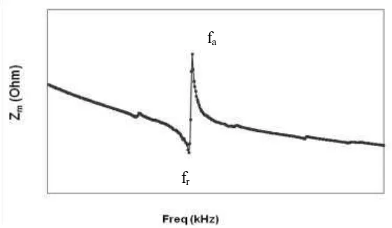
fr and antiresonant, fa frequencies which are influenced by the dimensions of the
[image:31.595.147.428.251.415.2]material and the clamping condition. When excited at the resonant frequency, the ceramic will resonate with greater amplitude which corresponds to the lowest impedance and follow by an antiresonant frequency, where the amplitude of the oscillation become minimum, which corresponds to the highest impedance in the circuit as shown in Figure 2-4.
Figure 2-4: Impedance of a piezoelectric ceramic at resonance.
As the thickness of the samples was many times smaller than their widths and lengths (h
< w/50 and h < l/100), this method is suitable for measuring the piezoelectric constants related to transverse modes, where the direction of polarisation is perpendicular to the direction of the applied stress. The transverse piezoelectric charge coefficient is given as [19]
(2-4)
This is related to the resonant frequency, fr, the difference between resonant and
antiresonant frequencies, Δf, the length of piezoelectric material, lb, the density, , and
the permittivity of the piezoelectric materials. 33T is the permittivity of the material, and
usually compared with the permittivity of vacuum, 0 (8.85 10-12 F/m) and described
in a form of relative dielectric constant at constant stress, K33T. This value is related to fr
fa
2 8 1 2
1
2 33 31
f f f
l d
r T
r b
the dimensions (thickness, h and area, A) of the piezoelectric material and its capacitance, CT (at constant or no stress) as
(2-5)
The effectiveness of energy conversion between electrical and mechanical is indicated by the coupling factor, which can be determined using
(2-6)
where is the elastic compliance at a constant electrical field of the material, which is the inverse of Young’s modulus, is measured at constant electric field (denoted as superscript E) and along its length (denoted as subscript 11) and can be estimated as
(2-7)
Once the coupling factor is known, the constant displacement elastic compliance, s11 D
(m2/N) can be calculated, which is related to the elastic compliance at constant electric field at a normalisation factor of coupling coefficient as
(2-8)
Other important piezoelectric properties are piezoelectric voltage coefficient, g31
(Vm/N), which is defined as the ratio of the charge coefficient to the permittivity of the material,
(2-9)
and the Q-factor of the piezoelectric material, Qm, can be determined by measuring the
equivalent resistance (minimum impedance, Zm) at the resonant frequency [21],
(2-10) 0 0 33 33 A h C K T T T
1 312
1111 s k
s D E
33 31 31 T d g
2 2
2.2.3
Piezoelectric Materials
There are a wide variety of piezoelectric materials. Some naturally exist in the form of crystals like Quartz, Rochelle salt, and Tourmaline group minerals. Some poled polycrystalline ceramics like barium titanium, and lead zirconate titanate, PZT, and polymer piezoelectric materials like polyvinylidene fluoride, PVDF and polyimide can be manufactured and easily integrated with MEMS [9].
Commercially, piezoelectric materials are manufactured in bulk form. They are fabricated from a combination of ceramic materials (in short piezoceramics) and pressed in a high temperature (1100 – 17000C) to form a solid poly-crystalline structure. The raw material to fabricate bulk piezoelectric is in powder form. The powder is then pressed and formed into desired shapes and sizes, which is mechanically strong and dense [21]. In order to make these bulk ceramics into piezoelectric materials, electrodes are deposited onto their surface either by screen printing or vacuum deposition, and poled with electric fields of 2-8 MV∙m-1 in an oil bath at a temperature of 130 - 220 0C [22]. Bulk piezoceramics are attractive for their high electromechanical efficiencies and high energy densities. However, bulk piezoceramics tend to be relatively thick (greater than 100 m), which will not be sensitive and need higher energies to actuate their structures, besides that they are difficult to be processed into thickness below 100 m, therefore limit their application in Micro-Electro-Mechanical System (MEMS) . Furthermore they need to be attached to certain parts of the MEMS structures using mechanical or adhesive bonding, which is tedious and not cost effective. MEMS devices which require piezoelectric structures with features below 100 m would usually be fabricated using thin and thick film technologies.
they are usually processed with a punching technique based on a micro-embossing technique which is described in the literature [24]. With the development of PVDF thin-film technology, micro-structures can be fabricated as reported by Arshak et al [25]. The fabrication process involved drying and curing at low temperature of around 170 C, and was able to produce d33 of 24 pC/N1 [26]. An alternative to PVDF is polyimide,
a high temperature piezoelectric polymer, which can maintain its piezoelectric properties at temperature up to 150 °C as reported by Atkinson et al [27].
Film piezoceramics have the advantages that lie between bulk and polymer piezoelectric materials. Although film piezoceramics do not have piezoelectric activity as high as bulk piezoceramics, however, for certain applications where a device thickness has to be fabricated less than 100 m, film piezoceramics are more favourable for their fabrication compatibility with micro scale devices. Films can be deposited directly on to a substrate, using a deposition technique that is more precise and with higher resolution. The processing temperature of film piezoceramics is in between bulk piezoceramics and piezoelectric polymers (800 °C – 1000 °C), which make it possible to be integrated with semiconductor technology. Film piezoceramics basically can be fabricated with thin- and thick-film technologies. Thin-film technologies involve physical vapour deposition, chemical vapour deposition, and solution deposition, which fabricate films with typical thickness less than 5 m. For thicker films (10 m – 100 m), thick-film technology is preferable. The technology involves a screen printing method, where each layer of ceramic thick film will be printed on a substrate followed by drying and curing processes.
2.2.4
Lead Zirconate Titanate (PZT)
Thick-film PZT materials can be classified as ‘hard’ and ‘soft’, according to their coercive field during field-induced-strain actuation and Curie temperature [30]. A ‘hard’ piezoceramic has larger coercive field (greater than 1 kV/mm) and higher Curie point (TC > 250 C) compared to ‘soft’ piezoceramic, which has moderate coercive field
(between 0.1 and 1 kV/mm) and moderate Curie point (150 C < TC < 250 C) .
Examples of ‘hard’ PZTs are Pz26 from Ferroperm Piezoceramics [22] and PZT-401
from Morgan Electroceramics [31]. Their typical applications are high power ultrasonics for cleaning, welding and drilling devices. Their distinctive characteristics include high mechanical factor, high coercive field, and low dielectric constant, which make them capable to be used in underwater applications and high voltage generators.
Compared to its counterpart, ‘Soft’ PZTs have lower mechanical Q-factor, higher
electromechanical coupling coefficient, and higher dielectric constant, which are useful to fabricate sensitive receivers and applications requiring fine movement control, for instant in hydrophones and ink jet printers. Other applications ranging from combined resonant transducers (for medical and flow measurements) to accelerometer and pressure sensors [32]. Examples of soft PZTs are Pz27 and Pz29 from Ferroperm Piezoceramics. Pz27 and Pz29 have similar properties as PZT-5A and PZT-5H respectively from Morgan Electroceramics [31] (Appendix A).
2.3
Piezoelectric Applications
The applications of piezoelectric materials can be categorised into sensors, actuators, transducers and generators depending on the type of piezoelectric effect. Sensors make use of the direct piezoelectric effect, transforming mechanical energy into measurable voltage signal. If the output power from this conversion is large enough to power microelectronic devices, it can therefore be used as a microgenerator. Actuators transform electrical into mechanical energy by means of the inverse piezoelectric effect. Finally, transducers use both effects to operate as single devices.
thin quartz crystals glued between two steel plates, and a hydrophone to detect the returned echo.
The successful practical use of piezoelectricity in sonar created intense development interest in piezoelectric devices. Over the next few decades, new piezoelectric materials and new applications for those materials were explored and developed, for instance, in 1927 Morrison and Horton demonstrated the Quartz crystal clock [34], which had been developed into various modern day applications such as computers, calculators, digital watches and mobile phones.
With the rapid development in micro-fabrication technology, microscopic devices based on piezoelectric materials were able to be fabricated. One of the earliest examples is the piezoelectric cantilever developed by Blom et al [35]. They used ZnO as the piezoelectric material to sputter on CVD (Chemical Vapour Deposition) SiO2. Later, Lee et al [36] used the method to develop a piezoelectric acoustic transducer for the application of highly sensitive micro-phone and micro-speaker.
Due to piezoelectric direct energy conversion between the electrical domain and the mechanical domain and thus prompt response (~ns), the application of piezoelectric materials has expanded into the detection of atomic masses. Itoh et al [37] had developed the first self-excited force-sensing micro-cantilever for dynamic scanning force microscopy (SFM). The devices have two piezoelectric ZnO layers on a SiO2 film. One of the layers was utilised for excitation and detection of the lever and the other for its static deflection. Yi et al [38] reported both experiment and theoretical investigations of the resonance frequency change of a piezoelectric unimorph cantilever due to the mass loaded at the tip of the cantilever, which is possible for bio-sensing applications.
thick piezoelectric ceramic bonded to a bonze disc of 0.25 mm thick with a diameter of 27 mm. They found that the optimum efficiency of the impact excitation approach is 9.4
% into a resistive load of 10 kΩ with most of the energy being returned to the ball
bearing which bounces off the transducer after the initial impact.
The interests in energy harvesting increased with advances in wireless technology and low power electronics. Piezoelectric materials are used to fabricate micro-generators which are able to capture the ambient vibration energy surrounding the electronics and converting this into usable electrical energy to power microelectronic devices. The application of energy harvesting is not limited to the ambient environment; it is also possible to harvest energy from human body. One such example is a shoe-mounted piezoelectric developed by Shenck et al [40]. They explored two methods, one of which is by harnessing the energy dissipated in bending the ball of the foot, using a flexible, multi-laminar PVDF bimorph stave mounted under the insole. The second one is to harness foot strike energy by flattening curved, pre-stressed spring metal strips laminated with a semi-flexible form of piezoelectric PZT under the heel, consisting of two back-to-back single-sided unimorphs. The PVDF transducer produced an average power of 1.3 mW when driving a 250 kΩ load at a 0.9 Hz walking pace, while the PZT transducer produced an average power of 8.4 mW in a 500-kΩ load at the same walking pace.
The examples given above are by no means an exhaustive list of piezoelectric applications. The range of piezoelectric materials applications are far too large to be covered in this work, therefore to suit the purpose of the study, piezoelectric materials fabricated in the form of cantilevers for the application of vibration energy harvesting will be discussed in detail.
2.4
Vibration Energy Harvesting
application of embedded and remote systems [42]. Micro-generator is the term often used to describe a device which produces electrical power in micro-Watt scale, while energy harvester is a more general term for describing a device which produces power derived from external ambient sources (e.g. solar, vibration, thermal and wind energy). Both of these terms will be used interchangeably in this book where appropriate.
The vibration energy harvesting of piezoelectric materials is based on the concept of shunt damping to control mechanical vibration [43], however, rather than dissipating the energy through joule heating, the energy is used to power some electronic devices.
In order to estimate the output power from a vibration energy harvester, analytical models have been developed over the years. A generic energy conversion model followed by a specific conversion model for piezoelectric will be discussed in the following section.
2.4.1
Generic Mechanical-to-Electrical Conversion Model
[image:38.595.202.377.502.635.2]One of the earliest general models for energy harvesters was proposed by William and Yates [44]. The model is represented as a single-degree-of-freedom linear mass-spring-damper system as illustrated in Figure 2-5.
Figure 2-5: A schematic diagram of a spring-mass-damper system of a piezoelectric FSD, based on the model developed by Williams et al [44].
When the system with lump mass, M is excited with a displacement of y(t) relative to the system housing, a net displacement z(t) is produced and the generic equation derived from Newton’s second law can be written as in equation (2-11), with the assumption
k
z(t)
y(t)
be bm
that the source of the vibration is unlimited and unaffected by the system. The general single degree of freedom model can be written as,
(2-11)
where is the spring constant. For a piezoelectric device, the damping effect of the system is related to its induced damping coefficient, b (with subscripts e and m referring to electrical and mechanical damping respectively), which can be written in relation to damping ratios, and undamped natural frequency, n as,
(2-12) As the system undergoes harmonic motion relative to the base with external excited displacementy(t)Ysin(t), there is a net transfer of mechanical power into electrical power. By solving the equation (2-11) andP bez
2 1
(electrical induced power), the
magnitude of the generated electrical power can be written as,
(2-13)
where T is the total damping ratio (T = e + m), and is the base excited angular frequency and Y is the amplitude of vibration. When the device is operated at its resonant frequency n, maximum power can be produced and equation (2-13) is
simplified to,
(2-14)
where ain is input acceleration from vibration source (ain n2Y). This equation shows
that input acceleration is the major factor for increasing the output power from the piezoelectric FSDs. By maintaining the frequency of the vibration source to match the
( ) ( ) ( ))
(t b b z t z t My t
z
M e m
m e n m
e M
b, 2 ,
2 2 2 2 3 3 1 2 n n T n e Y M P
22 max
4 n e m
natural frequency of the device, the electric power generated by the device is proportional to the square of the source acceleration.
2.4.2
Analytical Model of Piezoelectric Harvester
Although the mass-spring-damper system with lumped parameters is more suitable to represent a simple electromagnetic vibration-to-electric energy conversion model, it gives an insight of a general mechanism of mechanical to electrical transduction model which include piezoelectric transduction.
A more specific piezoelectric energy harvester model, where the mechanism of piezoelectric transduction due to the constitutive relations according to equation (2-1) is taken into account, has been proposed by duToit et al [45], with an additional term related to undamped natural frequency, n, piezoelectric charge constant, d33 and output
voltage, v being added to the single-degree-of-freedom equation (2-11). However, the model does not give a clear picture of optimum load resistance at resonant frequency. An improved model by Roundy et al [12] suggested an analogous transformer model representing the electromechanical coupling, while the mechanical and the electrical domains of the piezoelectric system are modelled as circuit elements, as shown in Figure 2-6.
Figure 2-6: A diagram of an analogous circuit for a piezoelectric vibrated device with a resistive load.
The mechanical domain of the equivalent circuit consists of inductor, resistor and capacitor which represents the mass of the generator, M, the mechanical damping, bm,
and mechanical stiffness, e respectively. At the electrical domain, C is the capacitance σin
+ _
M bm eT n
Cp R V
+
_
of the piezoelectric and R is the external resistive load, while n is the equivalent turn ratio of the transformer which is proportional to the piezoelectric charge constant d31. V
is the voltage across the piezoelectric and i is the current flow into the circuit, which are analogues to the stress and the strain rate respectively. The output voltage at resonant frequency derived from the model is,
(2-15)
where j is the imaginary number, is the driving frequency (Hz), r is the fundamental
resonant frequency of the cantilever (Hz), ET is the elastic constant for the composite
structure (N/m2), d31 is the piezoelectric charge coefficient (C/N), hP is the thickness of
the piezoelectric material, is the dielectric constant of the piezoelectric material (F), B
is a constant related to the distance from the piezoelectric layer to the neutral axis of the structure, T is the total damping ratio, k31 is the piezoelectric coupling fact
![Figure 2-5: A schematic diagram of a spring-mass-damper system of a piezoelectric FSD, based on the model developed by Williams et al [44]](https://thumb-ap.123doks.com/thumbv2/123dok/583553.69425/38.595.202.377.502.635/figure-schematic-diagram-spring-damper-piezoelectric-developed-williams.webp)
![Figure 2-7: Design of prototype generator (after [5]).](https://thumb-ap.123doks.com/thumbv2/123dok/583553.69425/44.595.86.500.372.583/figure-design-of-prototype-generator-after.webp)
![Figure 2-9: MEMS micromachined IDE pattern cantilever (after [15]).](https://thumb-ap.123doks.com/thumbv2/123dok/583553.69425/45.595.218.401.315.462/figure-mems-micromachined-ide-pattern-cantilever.webp)
![Figure 2-16: Fabrication steps for a ‘flip-and-bond’ technique [87].](https://thumb-ap.123doks.com/thumbv2/123dok/583553.69425/57.595.64.500.356.719/figure-fabrication-steps-flip-bond-technique.webp)
![Figure 2-17: Piezoelectric polyimide free-standing structure fabrication steps [27].](https://thumb-ap.123doks.com/thumbv2/123dok/583553.69425/58.595.99.452.357.570/figure-piezoelectric-polyimide-free-standing-structure-fabrication-steps.webp)