New approach FPGA-based implementation of
discontinuous SVPWM
Tole SUTIKNO1,2, Auzani JIDIN1,3, Nik Rumzi Nik IDRIS1
1Department of Energy Conversion, Faculty of Electrical Engineering
Universiti Teknologi Malaysia (UTM), Johor-MALAYSIA
2Department of Electrical Engineering, Faculty of Industrial Technology
Universitas Ahmad Dahlan (UAD), Yogyakarta-INDONESIA
3Department of Power Electronics and Drives, Faculty of Electrical Engineering
Universiti Teknikal Malaysia Melaka (UTeM), Melaka-MALAYSIA e-mail: [email protected], [email protected], [email protected]
Abstract
The discontinuous space vector pulse-width modulation (DSVPWM) is a well-known technique offering lower switching losses than continuous SVPWM. At the same, average switching frequency, or a switching frequency 1.5 times higher than utilized in continuous SVPWM, the discontinuous SVPWM results in lower current harmonic distortions than that obtained in continuous SVPWM at high modulation indices. This paper is concerned with the design and realization of new FPGA approach based a 5-segment discontinuous SVPWM operated at 40 kHz switching frequency. It will be shown that the implementation of the discontinu-ous SVPWM utilized in FPGA, to execute some complex tasks, is simplified through this new straightforward approach. For example, the judging of sectors, the computation of on-duration or firing pulses to control the switching of power switching devices can be executed much simpler with the proposed arithmetic logics or digital calculation in FPGA. In this way, the sampling frequency and hence switching frequency be increased. The SVPWM scheme has been implemented successfully based on APEX20KE Altera FPGA considering hardware resource saving. The validity of the proposed scheme has been tested experimentally to drive a 1.5 kW induction machine with low current harmonic distortions.
Key Words: Discontinuous SVPWM, hardware resource saving, FPGA
1.
Introduction
because SVPWM requires only a single-voltage reference rather than three voltage reference needed in SPWM, and the output inverter voltage in the SVPWM can be gradually controlled from PWM to a six-step mode. Moreover, SVPWM can achieve better current total harmonic distortion factor [1–4].
In common engineering practice, the SVPWM algorithm is implemented utilizing digital signal processors (DSP), which are superior in their ability to handle calculations involving trigonometric or complex algorithms. The DSP control procedure is performed sequentially, exploiting mathematically oriented resources. This may result in a slower cycling period if complex algorithms are involved. Thus, a purely software-based technique is not an ideal solution. Employing Field Programmable Gate Arrays (FPGA) in implementing SVPWM strategies provides advantages such as rapid prototyping, simpler hardware and software design, high speed computation and hence fast switching frequency. In contrast, FPGA performs entire procedures with concurrent operation (parallel processing via hardware) using reconfigurable hardware. For its powerful computation ability and flexibility, the FPGA may be the best solution to achieve excellent performance in ac drive systems. Currently, the FPGA has gained popularity and is widely used in many electric drive systems and in implementations of the SVPWM algorithm [2, 5–8].
It has been reported that continuous SVPWM suffers drawbacks such as computational burden, inferior performance at high modulation indices and high inverter switching losses. Hence to reduce the switching losses and improve performance in high modulation index regions, several discontinuous SVPWM methods have been proposed [9–12]. In this paper, the implementation of discontinuous SVPWM technique used for three-phase inverter utilizing FPGA is presented. The complex discontinuous SVPWM algorithm is simplified based on the basic ideas reported in [4] and [12]. Our effort is to verify the simplified method and propose some new techniques in defining the sector of space voltage vector and calculation the on-duration of PWM signals. It will be shown that the simple approach to design discontinuous SVPWM results in high speed in computing the overall algorithm and hence produce high switching frequency and low current harmonic distortions in the induction motor drive system. The validity of the proposed control method is verified by the experimental results of an induction motor drive system.
2.
The principles of SVPWM
The SVPWM was originally developed as a vector approach to pulse-width modulation (PWM) for three-phase inverter [1]. It is a more sophisticated technique for generating sinusoidal wave that provides a higher voltage to the motor with lower total harmonic distortion. It confines space vector to be applied according to the region where the output voltage vector is located. It is based on the fact that there are only two independent variables in a 3-phase voltage system. We can use orthogonal coordinates to represent the 3-phase voltage in the phasor diagram. A three-phase-voltage vector can be expressed as:
Vref =
states of the inverter are represented as 2 null vectors and 6 active vectors. These latter vectors (V1∼V6) can
be used to frame the vector plane, as illustrated in Figure 1. The rotating reference vector can be approximated in each switching cycle by switching between the two adjacent active vectors and the zero vectors. In order to maintain the effective switching frequency at a minimal value, the sequence of the toggling between these vectors is organized in such way that only one leg is affected in every step.
V3(010) V2(110)
Figure 1. Vector plane frame with (a) space voltage vectors, and (b) the decomposition of Vref in terms of Vkand
Vk+1 (e.g., in sector I).
Table 1. Criterion for sector identification as used in Reference [6]. Sector Vector Angle Vα, Vβ conditions
I (0◦, 60◦) 0≤V
The sector determination and application time of an active vector for all SVM strategies are the same. From Figure 1(a), it is obvious that the sector number is determined by the angle of the reference vector. Identification of sector k can be, generally, in αβ coordinates by using the appropriate boundary condition as per Table 1.
2.2.
Determination of the duration of active vectors
equation:
where Tkand Tk+1 are the dwell time of Vkand Vk+1 during each sampling period, respectively, and k is the
sector number denoting the reference location. For example in sector I, k=1, vector V1activates lasting for
T1, and V2activates lasting for T2 during T. The principle is similar in all sector of the six sectors, therefore
Figure 1(b) highlights the relation for sector I only.
Considering that magnitude of non zero space satisfies ||Vk|| = 2Vdc/3, the dwelling time can be evaluated by the following equations:
⎧
Here, Vdc is the dc-link voltage of the inverter, and T0 is the switching duration of a zero vector in each
sampling period. Suppose the reference is keeping a circular trajectory, the T0 >0, the output voltage is a
regular sinusoidal in linear modulation. As in equation (3), it is theoretically simple but it is obvious that this algorithm requires complicated computations involving trigonometric functions.
2.3.
Switching sequence (switching pattern)
This SVPWM strategy aims to minimize harmonic distortion in the current by selecting the appropriate switching vectors and determining of their corresponding dwelling widths. The flux produced by the reference voltage vector in a SVPWM switching period is a combination of each individual flux resulted by corresponding voltage vector.
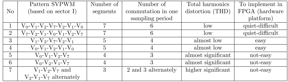
Table 2. Comparison of SVPWM patterns.
Pattern SVPWM Number of Number of Total harmonics To implement in No (based on sector I) segments commutation in one distortion (THD) FPGA (hardware
sampling period platform)
7 V1-V2-V7 and 3 2 and 3 alternately higher significant not-easy
V2-V1-V7 alternately
that SVPWM third and fourth patterns are easier to implement FPGA compared to others patterns. Moreover, those patterns have lower switching loss compared to 7-segment continuous SVPWM with almost low harmonics distortion.
3.
A new approach to implementing 5-segment discontinuous SVPWM
algorithm
Different from how SVPWM has been implemented by other previous researchers, this section presents a symmetrical 5-segment discontinuous switching sequence with a new method of sector determination and a new method of SVPWM generation based on calculation of active vector duration to avoid complicated computations with trigonometric functions, as mentioned in equation (3).
3.1.
Proposed SVPWM switching Pattern (5-segment discontinuous switching
pulses)
There has been reported many discontinuous SVPWM patterns [5, 9–11, 13]. However, not all those patterns have lower switching losses. A simpler algorithm, with low switching losses, can be easily implemented via FPGA. In this paper, a novel symmetric 5-segment discontinuous SVPWM design is considered, with reference to the basic idea from [4] and [12], in which is proposed there is always one channel that stays constant for the entire PWM period. The state sequence in this pattern is X-Y-Z-Y-X, where Z=1 in sector I, III and V, and Z=0 in the remaining sector. So the amount of switching time for this pattern is less than the continuous pattern. The obvious result of this is reduced switching losses.
A similar pattern has been successfully implemented via DSP by Yu [12]. That method has lower switching losses, a simpler algorithm and ease of implementation. Unfortunately, the implementation of a SVPWM algorithm based on DSP is limited to sampling rate and switching frequency, a limitation that can be expected because the DSP is a software-platform based device.
Therefore, this paper proposes using a FPGA, which is a hardware-platform based device, to improve sampling rate and switching frequency in the implementation of SVPWM.
3.2.
Proposed identification of the sector
Several methods have been introduced to decide the sector in which the reference space voltage vector lies. Zhi-pu [14] compared the reference space vector’s angle with 0◦, 60◦, 120◦, 180◦, 240◦, and 300◦ to obtain
the sector number in which Vreflies. Others, Yu [15], Jiang [7] and Xing [16], have analyzed the relationship between Vαand Vβ to determine the sector. They have calculated the projections Va, Vb and Vc of Vαand Vβ in (a,b,c) plane by using the inverse Clark transformation:
⎧
⎪ ⎨
⎪ ⎩
Va=Vβ Vb=
√
3Vα−Vβ
2
Vc =− √
3Vα−Vβ
2 .
(4)
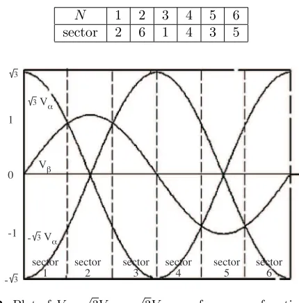
N 1 2 3 4 5 6
3Vα waveforms as a function of time.
Table 3. The proposed, simpler identification of the sectors. 1 denotessatisfy, 0 denotesnotsatisfy. Sector Vector Angle Vβ >0 Vβ>
3Vβ, as decomposition of continuous SVPWM, which will properly counteract the redundant calculations to identify sector location; but it imported complicated matrix calculations. Hence, through analyzing SVPWM, as mentioned above, the present work has
created a simpler method to determine the sectors of voltage vectors based on comparison between Vβ,
√
3Vα,
−√3Vα and 0, as shown in Figure 2. With the comparison, we can more simply determine the voltage-vector sectors compared to [7, 14–17]. Table 2 clarifies sector identification via truth table.
3.3.
The proposed calculation of the duration of active vectors
In this work, based on the analysis performed in [12], a new set of equations to calculate the duration of active vectors for each sector has been rearranged in order to construct an easier implementation based on FPGA. The equations associated with each sector are shown in Table 3.
3.4.
Proposed method to generate SVPWM switching pulses
can be adopted in the proposed SVPWM. To simplify the implementation based on FPGA, a graphical method has been devised to generate the SVPWM switching pulses as illustrated in Figure 3.
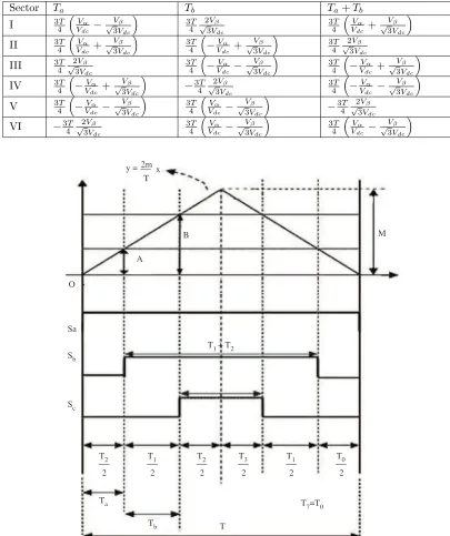
Table 4. The switching time of the active vector for each sector.
Sector Ta Tb Ta+Tb
Figure 3. Proposed method to generate SVPWM switching pulses. Considering the relation y = 2m
pulses was set equal to 1. For even sector positions, PWM generation was implemented via complement of comparison between triangle and Ta, and complement of comparison between triangle and Ta +Tb; other switching pulses were set equal to 0.
For example, in sector I, if x=Ta=T20, then y= 2m
T
T0
2
; and if x=Tb= T21, then y= 2m
T
T1
2
. For
simpler circuit design, in this paper the term 2m
T is set equal to 1; so if x= T0
2 =Ta, then y =
T0
2 =Ta; and
if x= T1
2 , then y=
T1
2 =Tb. Obviously, if x=
T0
2 +
T1
2 =Ta+Tb then y =
T0
2 +
T1
2 =Ta +Tb. Therefore,
the generation of PWM for channels Sb and Sc in sector I can be obtained comparing the triangle with Ta, and comparing triangle and Ta+Tb, respectively, with channel Sais set equal to 1. The generation of PWM in other sectors can be obtained in a similar way.
4.
FPGA implementation of a proposed novel SVPWM
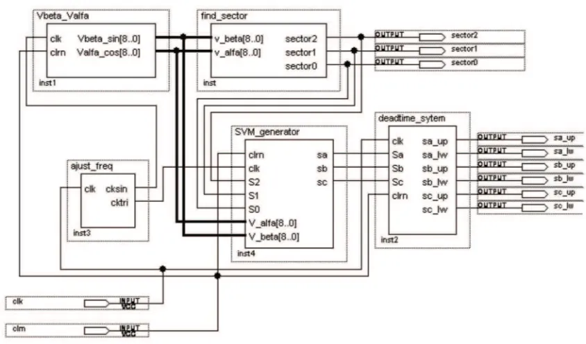
In the previous section, the principle of SVPWM was analyzed. In this section, implementation of the proposed SVPWM based on FPGA is presented. An overall schematic of the proposed SVPWM design is shown in Figure 4. The overall block is divided into 5 sub-modules: ajust freq,Vbeta Valfa,find sector,SVM generatorand the
deadtime system module.
Figure 4.An overall schematic of the proposed SVPWM design.
4.1.
Adjustable frequency module
to 50 Hz. To get the desired carrier and reference signal frequency, the clock frequency is divided. For example, to generate a 40 kHz carrier signal sampled 32 times, the source clock generator (L6) is divided by 26 (33.33 MHz : 26 : 32 = 40 kHz). The reference signal clocking is produced in a similar way.
Figure 5. Modules Vα and Vβ.
4.2.
V
αand V
βmodule
In this work, Vα and Vβ are generated through a sine and cosine look-up table (LUT) function with memory mapping 360 entries. The lower, base, and higher numbers of sine and cosine function are 96, 224 and 352 respectively (in 9 unsigned bits). The design of modules Vα and Vβ are shown in Figure 5. Because in this design uses 360 memory mapping addresses, then a counter mod-360 is used to count LUTs mentioned above. As a note, in advanced close-loop control Vα and Vβare obtained the ABC to αβ transformation of voltage sensing.
4.3.
Sector identification module
The Sector Identification module is used to determine sector based on Table 2. The design of sector identification is shown in Figure 6.
The sub-modules denoted “x pos akar” and “x neg akar” were used to multiple between Vα by
√
3 and
Vα by −
√
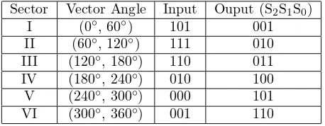
3 , respectively; then, those results were compared with Vβ through sub-module “comp9a,” written in VHDL code, and Vβ was compared to zero through sub-module “compa,” as shown in Figure 6. The simplification of truth table for comparison results, as shown in Table 5, were used to determine sector number in sub-module “csector.”
Table 5. Conversion of comparison result between Vβ,
√ 3Vα,−
√
3Vαand 0 to sector number.
Sector Vector Angle Input Ouput (S2S1S0)
I (0◦, 60◦) 101 001
II (60◦, 120◦) 111 010
III (120◦, 180◦) 110 011
IV (180◦, 240◦) 010 100
V (240◦, 300◦) 000 101
Figure 6. Sector identification module.
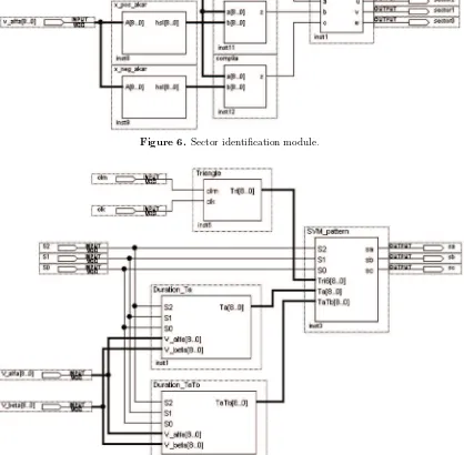
Figure 7. Three phase SVPWM signal generator module.
4.4.
Three-phase SVPWM signal generator module
The overall schematic for the three-phase SVPWM signal generator module is shown in Figure 7. This module can be divided into 4 sub-modules, namedTriangle,Duration Ta,Duration TaTb, andSpace Vector Modulation
between 224 and 352. Sub-modulesDuration Ta andDuration TaTb were created based on digital solution of the second and fourth columns in Table 3, respectively. Sub-moduleSVM pattern was used to generate the set of SVPWM pulses; refer to Section 3.4 and Figure 3.
5.
Simulation and experiment results
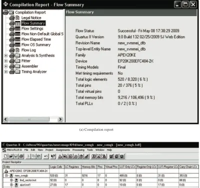
The software to design, perform compilation, verification and develop hardware based on the APEX 20KE FPGA was developed under the Alterus Quartus II, Version 9.0, Web Edition.
(a) Compilation report
(b) The using of FPGA resource in detail
5.1.
Simulation
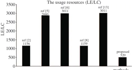
In this work, we set Vdc/T = 1, switching frequency to 40 kHz, and reference frequency to 50 Hz. The Quartus II compilation report for the proposed SVPWM generator is shown in Figure 8(a), and further detail for each module shown in Figure 8(b). It can be seen that the design requires 520 logic elements and 9,216 memory bits. When compared with other previous methods, the proposed method required the minimum hardware resources, as shown in Figure 9.
3500
3000
2500
2000
1500
1000
500
0
LE/LC
methods
ref [2] 1156
ref [5] 2880
ref [6] 3011
ref [8] 1159
ref [13] 3011
proposed 520
The usage resources (LE/LC)
Figure 9. The comparison of required hardware resources.
The simulation result in sector I and II of the proposed SVPWM is shown in Figure 10. This simulation result has proved that the proposed design runs as desired as in [10, 12].
Figure 10.Simulation results of the proposed SVPWM generator.
5.2.
Experiment
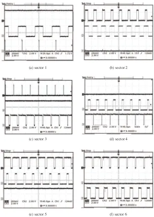
The previous section has shown that the proposed SVPWM generator runs properly at simulation level. Next is to validate the design at hardware level. In this work, the proposed SVPWM generator design, with carrier frequency 40 kHz, was successfully programmed into the Altera APEX 20KE FPGA. The shape of switching state pulses in each sector and the 2 µs dead-time are shown in Figures 11 and 12 respectively. These results show that the design runs as desired and as in [10, 12].
(a) sector 1 (b) sector 2
(c) sector 3 (d) sector 4
(e) sector 5 (f) sector 6
Figure 11. Shape of switching state pulses in each sector.
(a) The shape of swiching state pulses in sector 2
(b) The zoomed dead time of Sa swiching state in sector 2
Figure 12. The shape of dead-time pulses for the proposed SVPWM generator in sector 2. Image (b) is zoom of the image in (a).
(a) The swithcing state and its line-to-line (b) The signal gating and its frequency spectrum
Figure 13. The hardware implementation of the proposed SVPWM generator. at carrier frequency 40 kHz. We have also tested the proposed FPGA based SVPWM generator design using a three-phase voltage
source inverter connected to a 1.5 kW load. The results are shown in Figure 14(a) ˘G(d). The figure shows the phase and line voltages, the phase current and the frequency spectrum of the phase current. The practical results from the test-rig were in as expected and showed that the proposed SVPWM generator design has successfully driven a 1.5 kW induction machine, with low current ripple.
6.
Conclusion
functions). The SVPWM scheme has been implemented successfully based on the Altera APEX 20KE FPGA. It also has been tested successfully to drive a 1.5 kW induction machine, exhibiting low current ripple.
(a)line voltage and phase current (b) frequency spectrum of the phase current
(c) 3-phase currents (d) line to neutral voltage
Figure 14. The performance of proposed SVPWM generator design based on FPGA.
Acknowledgments
The authors wish to acknowledge the Research Management Center (RMC) of Universiti Teknologi Malaysia (UTM) and the Ministry of Science and Technology Malaysia (MOSTI) for the financial funding of this project, and also the Laboratory of Advanced Machine Research, Department of Energy Conversion, Faculty of Electrical Engineering, Universiti Teknologi Malaysia (UTM).
References
[1] H. W. van der Broeck, H. C. Skudelny, and G. V. Stanke, “Analysis and realization of a pulsewidth modulator based on voltage space vectors,”Industry Applications, IEEE Transactions on,vol. 24, pp. 142-150, 1988.
[3] B. K. Bose,Modern Power Electronics and AC Drives. New Jersey: Prentice-Hall PTR, 2002.
[4] A. M. Trzynadlowski, R. L. Kirlin, and S. Legowski, “Space vector PWM technique with minimum switching losses and a variable pulse rate,” inIndustrial Electronics, Control, and Instrumentation, 1993. Proceedings of the IECON ’93., International Conference on, 1993, pp. 689-694 vol.2.
[5] T. Ying-Yu and H. Hau-Jean, “FPGA realization of space-vector PWM control IC for three-phase PWM inverters,” Power Electronics, IEEE Transactions on,vol. 12, pp. 953-963, 1997.
[6] Z. Zhaoyong, L. Tiecai, T. Takahashi, and E. Ho, “Design of a universal space vector PWM controller based on FPGA,” inApplied Power Electronics Conference and Exposition, 2004. APEC ’04. Nineteenth Annual IEEE, 2004, pp. 1698-1702 Vol.3.
[7] S. Jiang, J. Liang, Y. Liu, K. Yamazaki, and M. Fujishima, “Modeling and cosimulation of FPGA-based SVPWM control for PMSM,” inIndustrial Electronics Society, 2005. IECON 2005. 31st Annual Conference of IEEE, 2005, p. 6 pp.
[8] Y. Guijie, Z. Pinzhi, and Z. Zhaoyong, “The Design of SVPWM IP Core Based on FPGA,” inEmbedded Software and Systems Symposia, 2008. ICESS Symposia ’08. International Conference on, 2008, pp. 191-196.
[9] Z. Keliang and W. Danwei, “Relationship between space-vector modulation and three-phase carrier-based PWM: a comprehensive analysis [three-phase inverters],”Industrial Electronics, IEEE Transactions on,vol. 49, pp. 186-196, 2002.
[10] K. S. Gowri, T. B. Redd, and C. S. Babu, “Novel Space Vector Based Generalized Discontinuous PWM Algorithm for Induction Motor Drives,”ARPN Journal of Engineering and Applied Sciences,vol. 4 no.1, February 2009. [11] W.-F. Zhang and Y.-H. Yu, “Comparison of Thre SVPWM Strategis,”Journal of Electronic Science and Technology
of China,vol. 5 no.3, pp. 283-287, September 2007.
[12] Z. Yu, “Space-Vector PWM With TMS320C24x/F24x Using Hardware and Software Determined Swithing Pat-terns,” Texas Instruments Application Report SPRA524, March 1999.
[13] C. Bharatiraja, T. B. Prasad, and R. Latha, “Comparative Realization of Different SVPWM Schemes in Linear Modulation Using FPGA,” inIEEE Region 8 Sibircon, 2008, pp. 164-168.
[14] Z. Zhi-pu, “Design and Realization of Space Vector PWM Based on SG,”Drive and Control,vol. 7, pp. 29-32, 2005. [15] F. Yu, X. Yan, and H. Yuwen, “A fast algorithm for SVPWM in three phase power factor correction application,”
inPower Electronics Specialists Conference, 2004. PESC 04. 2004 IEEE 35th Annual, 2004, pp. 976-979 Vol.2. [16] S. Xing and K.-Y. Zhao, “Research on A Novel SVPWM Algorithm,” inIndustrial Electronics and Applications,
2007. ICIEA 2007. 2nd IEEE Conference on, 2007, pp. 1869-1872.
![Table 1. Criterion for sector identification as used in Reference [6].](https://thumb-ap.123doks.com/thumbv2/123dok/619850.74629/3.595.126.483.450.545/table-criterion-sector-identication-used-reference.webp)