PJP/2012/FKEKK(27B)S1030
DESIGNING ARTIFICIAL MAGNETIC CONDUCTOR USING
BENDABLE SUBSTRATE FOR METAL OBJECT DETECTION
IN RFID APPLICATION
DR MAISARAH BINTI ABU
FACULTY OF ELECTRONIC ENGINEERING AND COMPUTER
ENGINEERING
UNIVERSITI TEKNIKAL MALAYSIA MELAKA
PJP/2012/FKEKK(27B)S1030
DESIGNING ARTIFICIAL MAGNETIC CONDUCTOR USING
BENDABLE SUBSTRATE FOR METAL OBJECT DETECTION
IN RFID APPLICATION
DR MAISARAH BINTI ABU
FACULTY OF ELECTRONIC ENGINEERING AND COMPUTER
ENGINEERING
2013
Designing Artificial Magnetic Conductor for Metal Object Detection in RFID Application
(Keyword: Dipole antenna, artificial magnetic conductor, perfect electric conductor, bandwidth, return loss, gain)
Radio Frequency Identification, (RFID) is one of emerging technology nowadays. It is capable to handle more than one object in one time. Each object will be attached to the tag or transponder which is very small and thin. The tag is one of the important components in RFID system. It consistsof a dipole antenna anda tiny chip that will be used to store the data of the object. The problem in RFID system is whenever the tag is placed near to onto the metal surface (or object) it become invisible. The tag is failed to be detected by the reader‟s antenna because of the behavior of the metal that will reflect all signals received by the tag. Hence, it will change the return loss, gain and efficiency of the tag. In this project, the Artificial Magnetic Conductor, (AMC) is designed to overcome the problem caused by the metal object. AMC is placed at the back of the RFID tag to redirect back the reflected signal. Three types of AMC are designed at frequency of 920 MHz, 2.45 GHz and 5.8 GHz by using different types of substrate and structure. The process started by designing and simulating the design by using CST Studio Suite 2011. After getting the desired result, the design is fabricated onto the substrate using manual etching process. At the end of the process, the fabricated design will be tested using the actual RFID system from the manufacturer to get the maximum read range of the tag when applied to the AMC and metal object.
Key Researchers:
DrMaisarahBinti Abu (Head) Miss EryanaEiydaBintiHussin Assoc. Prof. Dr Abdul Rani Bin Othman
Mr. Fauzi Bin Johar
Mdm. Rose FarahiyanBintiMunawar Mdm. NorhidayahBintiMohdYatim
Tel no: 06-5552055
Vote No: PJP/2012/FKEKK (27B) S1030
ACKNOWLEDGEMENT
I acknowledge with gratitude to Centre of Research and Innovation Management (CRIM) of UTeMas the funder of this project. I wish to express my sincere thanks to my co-researcher, Assoc. Prof. Dr Abdul Rani Bin Othman,
Mr.Fauzi Bin Johar, Mdm. Rose FarahiyanBintiMunawar and
Mdm.NorhidayahBintiMohdYatim for their support and guidance in the project. I would like to thank my co-supervisor master student, Miss EryanaEiydaBintiHussin who helps me to complete the project as planned. I extend my gratitude to the Lab Technicians Mr.MohdAeini Bin Amin, Mr. Imran Bin Mohamed Ali and Mr.MohdSufian Bin Abu Talib for providing me all the necessary facilities in the lab. I place my sincere gratitude to all relatives, friends and all researchers who shared their support, morality and brilliant idea.
TABLE OF CONTEN T
2.3 Operational Frequency of RFID 6
2.4 Problem in RFID system 7
2.5 The Use of Artificial Magnetic Conductor in RFID System 8
2.5.1 Characteristic of Artificial Magnetic Conductor 8
2.6 Study on Artificial Magnetic Conductor with Dipole Antenna 10
2.6.1 Split-Ring Resonators AMC with Dipole Antenna 10
2.6.2 Square AMC with Wide-band Patch Antenna 12
2.6.3 AMC Loaded Monopole Antenna 14
2.7 The Use of AMC for RFID Tag Application 15
2.7.1 Low Profile RFID Tag and Compact Rectangular AMC
Substrate 16
2.7.2 Printed UHF RFID Tag Antenna for Metal Object 17
2.8 Summary 18
3.1 Basic Square AMC Unit Cell 20
3.2 Modification to Square Unit Cell AMC 20
3.2.1 Stacked Wafer AMC at 920 MHz 21
3.2.2 Halfring AMC at 2.45 GHz 24
3.3 Angle of Incidence 27
3.4 Dipole Antenna with AMC 29
3.4.1 920 MHz Antenna with Stacked Wafer AMC 29
3.4.2 2.45 GHz Antenna with Halfring AMC 30
3.5 Summary 32
CONCLUSION 33
LIST OF FIGURES
TABLE TITLE PAGE
1.1 Flow chart of project methodology 3
2.1 The components of RFID system 6
2.2 RFID frequency band in Electromagnetic Spectrum 7
2.3 RFID tag detection with antenna 7
2.4 Characteristics of Artificial Magnetic Conductor 8
2.5 Reflection phase graph 9
2.6 Side-view of AMC, FSS and EBG structure 9
2.7 Basic structure of AMC an equivalent circuit of basic
AMC structure
10
2.8 7x7 cell array MSRR AMC and return loss for dipole
when applied to PEC and AMC
11
2.9 7x7 cells MSRR AMC with dipole antenna at 2.4 GHz 12
2.10 Simulation result and side view of Square AMC with
Wide-band Antenna
12
2.12 Front view and side view of compact rectangular AMC 16
2.13 Simulation of finite and infini ground plane to RFID tag
antenna
16
2.14 Structure of mushroom-like AMC with three conducting
layer
17
3.1 Parametrci study on square patch AMC 20
3.2 The variation of slots introduced into the new design 21
3.3 Comparison of one slot and multiple slots size. 22
3.4 Reflection phase of square slot and plus shape slot at the
center of the patch
22
3.5 Thickness modification of AMC 23
3.6 The new of AMC at 920 MHz (a) front view (b) layer view 24
3.7 Parametric study for the length of square patch AMC 25
3.8 Illustration of square, rectangular and Halfring AMC 26
3.9 Parametric Study on Halfring AMC 27
3.10 Magnitude and reflection phase of Stacked Wafer AMC
when applied to incidence of angle from 0° to 60°.
28
3.11 Magnitude and reflection phase of Stacked Wafer AMC
when applied to incidence of angle from 0° to 60°.
29
3.12 Return loss and radiation pattern of 920 MHz antenna
when pplied to metal and Stacked Wafer AMC.
31
3.13 Fabricated Stacked Wafer AMC for 920 MHz RFID
application
LIST OF TABLES
TABLE TITLE PAGE
2.1 Comparison between active and passive tag 6
2.2 Comparison between single patch antenna and 2x2 array patch
antenna when applied to AMC ground plane
13
3.1 Size and bandwidth for square AMC at 920 MHz and 2.45 GHz 19
3.2 The performance of dipole antenna when applied to metal and
Stacked Wafer AMC.
30
3.3 Simulation result of 2.45 GHz antenna when applied to metal and
Halfring AMC.
LIST OF SYMBOLS
C - Capacitance
L - Inductance
R - Resistance
λ - Wavelength
- Upper frequency
� - Lower frequency
- Resonant frequency
BW - Bandwidth
� - Permittivity of free space
� - Dielectric constant
t - Substrate thickness
g - Gap between patches
W - Width
LIST OF PUBLICATIONS
Conference papers:
M. Abu, E. E. Hussin, A.R. Othman, N.M Yatim, F.M. Johar, R.F Munawar, Design
of Stacked Wafers AMC at 920 MHz for Metallic Object Detection in RFID
Application, 2013 IEEE Symposium on Wireless Technology and Application
(ISWTA), September 22-25, Kuching.
M. Abu, E. E. Hussin, A.R. Othman, N.M Yatim, F.M. Johar, R.F Munawar,
Designing Halfring Artificial Magnetic Conductor RFID Application, 2013 IEEE
LIST OF AWARD
Gold Medal – Use Of Artificial Magnetic Conductor In Radio Frequency
Identification, Malaysia Technology Expo (MTE), 21-23 February 2013.
Silver Medal - Use Of Artificial Magnetic Conductor In Radio Frequency
Identification, Seoul International Invention Fair 2013 (SIIF 2013), 28 Nov – 2 Dec
CHAPTER 1
INTRODUCTION
1.1 Introduction
1.2 Objective
The objective of this project is to design, simulate, fabricate and test the Artificial Magnetic Conductor at frequency of 920 MHz and 2.45 GHz with an improvement of gain, directivity and efficiency of the dipole RFID tag.
1.3 Scope of work
The project started by designing the one cell of AMC at each frequency of 920 MHz and2.45 GHz. Each AMC is designed using different types of substrate and structure. For 920 MHz AMC, the new structure called Wafer AMC is designed using Rogers RO3010 with thickness of 1.28 mm and dielectric constant of 10.2. Half ring AMC is designed at 2.45 GHz AMC using Rogers RO3003 with thickness of 1.52 mm and dielectric constant of 3. Then, each of the single unit cells will be combined with the low-profile dipole antenna and optimized at the each frequency represented. Once the design is confirm, it will be fabricate using chemical equipment. Finally, the AMC will be tested on the actual RFID system. The fabricated AMC will be attached to the RFID tag and the performance is measured.
1.4 Problem Statement
1.5 Project Methodology
CHAPTER II
LITERATURE REVIEW
2.1 History of RFID System
Radio Frequency Identification or RFID is one of emerging technology today. RFID is an evolution from the barcode scanning system. The special feature of RFID system is that it can read or detect the object contactless without the need of direct line of sight between the reader antenna and the object/s. This make RFID system as a big potential to attract many kinds of industries that related to item tagging and labelling such as inventory control, supply chain and library management.
The first application of RFID system developed by the British Royal Air Force during World War II by the “Identify Friend or Foe” (IFF) system which can detect enemies aircraft by the sending the RF signal. In 1980 shows the first implementation of full RFID system in world class country such as United States, Europe and Spain. The study of electromagnetic theory by R. F. Harrington stated in his paper “Theory of Loaded Scatterers” is one of the early researches on RFID in 1960s. Research on RFID is continued by J. H. Vogelman in his invention of “Passive data transmission technique utilizing radar echoes”. In 1970s the RFID system successfully attracts the intention of developers, government and some academic institutions [7].
integrated circuit and antenna on the RFID tag make it more useful especially for large-scale industry.
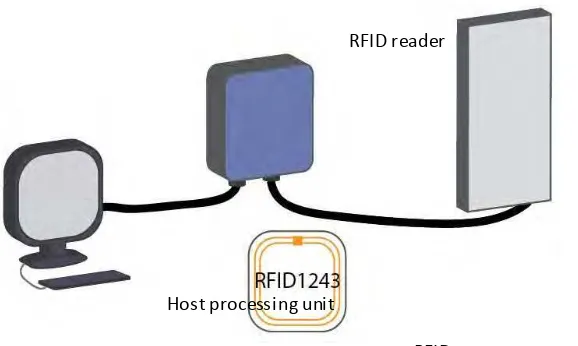
2.2 RFID Components
The basic components of RFID system consists of a tag, a reader and an antenna. The tag is a combination of programmable chip and dipole antenna. The RFID tag can be an active of passive types depending on the application. Mostly the users prefer to use passive tag because it is cheaper and smaller. However, the active tag may be good for large-scale industry that need security feature to their system such as supply chain. Table 1 shows the comparison between the active and passive RFID tag. The second component of RFID system is the reader. The reader is the one that will process all the data sent/receive to/by the antenna. It can be categorized into two types; fixed reader and handheld reader. Fixed reader comes with larger size and will be mounted at one point so it can read any tag that pass through it. While for handheld reader the size is smaller and it is supported with rechargeable battery. Usually the handheld reader is use to detect individual item at one time.The third component of RFID system is the antenna. The antenna communicates to the tag before it can send the data to the reader.
Figure 2.1: The component of RFID system.
Table 2.1: Table of comparison between active and passive tag.
Active RFID Passive
2.3 Ope rational Fre quency of RFID
Figure 2.2: RFID frequency band in Electromagnetic Spectrum
2.3 Proble m in RFID System
The passive tag need to be placed near to or passed through the antenna will become active. The tag will receive the electromagnetic wave from the antenna and resent some of it back. This process is called backscattering modulation. The characteristic of RFID system is defined by the performance of the antenna. Good antenna can give longer reading distance so it can capture more tag at one time. However, goodRFID tag also can help to increase the performance of the RFID system by increasing the possibility to be detected by the antenna.
Figure 2.3: RFID tag detection with antenna.
The use of passive tag is limited to some object or surface. The passive tag cannot be used for metal object identification because of the behaviour of the metal
RFID Antenna
that will reflect all the electromagnetic wave sent by the reader. Therefore, the chip inside the tag is not activated and it will stay invisible to the antenna. For metal object identification users are recommended to use the active RFID system but the cost is very high. Figure 2.3 shows three RFID tags at three different conditions. Tag A is placed within the detection area of antenna so it will receive the electromagnetic wave. Hence, the communication between the tag and antenna is successful. While Tag B is placed out of the detection area so it failed to receive the electromagnetic wave from the antenna. For Tag C even that it is placed within the detection area, but the tag is attach to the metal object. Therefore, the communication is failed.
2.4 The Use of Artificial Magnetic Conductorin R FID System
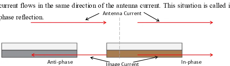
Artificial Magnetic Conductor or AMC is one of the metamaterial structure that been use in antenna design to increase the performance in term of gain and directivity. For RFID system that use of AMC can be applied to the reader‟s antenna or tag‟s antenna. AMC act as a ground plane of the antenna. For reader‟s antenna the AMC is use to replace the conventional ground plane. While for tag‟s antenna the AMC will be added at the back of the tag because it does not have ground plane. Figure 2.4 shows why the tag should not be attach to the ground plane (or metal layer). When tag is applied to metal object the antenna current and image current will cancelled out to each other. However, when AMC is use at the back of tag, image current flows in the same direction of the antenna current. This situation is called in-phase reflection.
Figure 2.4: Reflection of antenna current and image current for metal object and AMC when attach to the RFID tag.
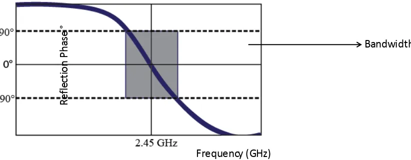
2.4.1 Characteristics of Artificial Magnetic Conductor
The term Artificial Magnetic Conductor is use because Perfect Magnetic Conductor (PEC) that exhibits novel electromagnetic properties is not exists in the
Antenna Current
Image Current
real world. Sometimes, it is also called as High Impedance Surface AMC (HIS-AMC) structure because its produce very high impedance at resonant frequency. The character of AMC is defined by the reflection phase graph with zero reflection phases and +1 magnitude at resonant state. The use of AMC can help to remove the unwanted signal to reduce amount of wasted power at the back hemisphere. Another character that defines AMC is the value of bandwidth. The bandwidth is defined by the shaded are in Figure 2.5 which is fall between ±90°. The value of bandwidth can be calculated using equation (1).
Figure 2.6: Side-view of (a) AMC (b) FSS and (c) EBG structure.
Figure 2.7: (a) Basic structure of AMC (b) equivalent circuit of basic AMC structure
Whereη, εandμare impedance, permittivity and permeability of free space, W is width of patch and g is gap between substrate and structural PEC patch layer. 2.5 Study on Artificial Magnetic Conductor with Dipole Antenna
This session will discuss about the effect of applying AMC to improve the performance and efficiency of the antenna. Three types of antenna will be discussed with different types of pattern and design approach.
2.5.1Split-Ring Resonators AMC with Dipole Antenna
RFID tag is designed using low-profile dipole antenna with minimized size and reduced cost. At the beginning of this research the effect of applying the AMC of dipole tag is studied. Previously in [10], the Split-Ring Resonator (SRR) is designed in with two ring patch with a split each ring. This paper shows that when the dipole antenna is placed on metal (or PEC) plane, the return loss dropped to -0.4 dB. By applying 7x7 SRR AMC, the return loss increased (in negative side) to -25.6 dB.Later in [11], the Multiple Split-Ring Resonators (MSRR) in square shape is designed at resonant frequency of 2.4 GHz with 7x7 and 9x9 cells array. Dipole antenna is designed at the same frequency with dimension of 2.4 mm x 56.37 mm. The use of MSRR AMC increased the return loss from-0.35dB (when applied to metal) to -15.2 dB and -13 dB for 7x7 and 9x9 cell array respectively.Figure 2.8(a) shows the 2.4 GHz dipole antenna with 7x7 cells MSRR AMC and (b) shows the return loss graph when dipole antenna is applied to PEC and MSRR AMC.
(a) (b)
Figure 2.8: (a) 7x7 cell array MSRR AMC (b) return loss for dipole when applied to PEC and AMC (reprint from [10])
(a) (b)
Figure 2.9: (a) 7x7 cells MSRR AMC with dipole antenna at 2.4 GHz.
2.5.2 Square AMC with Wide-band Patch Antenna
In [12], dual ground plane is used; the AMC ground plane and conventional ground plane. The AMC is placed at the back of the antenna to cover the patch side while the PEC ground plane is placed at the back of antenna feed line. This method
can reduce the width of feed line and can avoid unwanted spurious radiation. Therefore, the conventional ground plane (or PEC) is raised with the same height of
the AMC (Figure 2.10(b)). Firstly, 3 x 4 square AMC is used as a ground plane for single patch antenna and the realized gain increased by 18.48% and bandwidth by 66.32%. Figure 2.10(a) shows the simulated result of gain and return loss on single
patch antenna when applied to AMC and PEC accordingly. Then, 2x2 array patch antenna is designed to further increase the gain and bandwidth of the antenna element.
The comparison between single antenna and 2x2 array antenna is shows in Table 2.1. Again, the AMC is applied with 8x3 arrangement at left and right side of antenna ground plane. Now, the PEC ground plane is placed at the middle of antenna(at the


![Figure 2.8: (a) 7x7 cell array MSRR AMC (b) return loss for dipole when applied to PEC and AMC (reprint from [10])](https://thumb-ap.123doks.com/thumbv2/123dok/538866.62701/24.596.208.425.282.399/figure-cell-array-msrr-return-dipole-applied-reprint.webp)
