Design of Stacked Wafers AMC at 920 MHz for
Metallic Object Detection in RFID Application
M. Abu, E.E. Hussin, A.R. Othman, N.M. Yatim, F.M. Johar, R.F. Munawar. Universiti Teknikal Malaysia Melaka,
Hang Tuah Jaya, 76100 Durian Tunggal, Melaka.
Email: [email protected], [email protected], [email protected], [email protected], [email protected], [email protected]
Abstract – Artificial Magnetic Conductor, AMC is introduced into RFID application to overcome the problem of metal object detection. The AMC act as the Perfect Magnetic Conductor, PMC exhibits a reflectivity of +1 (in-phase reflection). In this paper, the stacked wafers AMC structure is designed to operate at 920 MHz frequency. The proposed stacked wafers AMC is an evolution from the basic square patch AMC. By introducing different size of slots into the square patch will help to reduce the frequency hence increase the bandwidth of the reflection phase. Another method to increase the bandwidth is by increasing the thickness of the structure. For the single cell of stacked wafers AMC proposed in this paper, the simulated bandwidth is 3.5% with reduced size of 45.56% than the square AMC. An optimized structure of 3x2 stacked wafers AMC give better return loss = -21.8 dB and gain = 3.04 dB with total efficiency of 82.3%.
Keywords-stacked wafers, bandwidth, frequency respond, artificial magnetic conductor,reflection phase, high impedance surface, dipole antenna
I. INTRODUCTION
Radio Frequency Identification (RFID) is one of emerging technology nowadays. It consist of three major part; a tag which will be mounted on the object, an antenna that will communicate to the tag, and a reader that connects to the antenna to proses the data send to or received by the tag [1]. The unique feature of the RFID tag that contactlessly respond to the antenna with no line of sight makes it useful for many kind of application such as for baggage handling in airport, books tracking in library and anti-theft system in hypermarket depends on its operating frequency. The RFID frequency lies between Low Frequency (125 KHz) until Microwave Frequency (24 GHz). UHF (Ultra High Frequency) RFID system is used for wide range application such as supply chain and security management. In any cases when RFID tag is placed near the metal or perfect electronic conductor (PEC) object the electromagnetic wave transmitted by the dipole tag will be reflected by the metallic object [2]. The value of gain
will be decreased and the efficiency of the tag’s antenna will be
very small (≈ 0%) which means that the tag cannot respond to
the reader. There are two ways to overcome this problem; either to add spacer or to introduce a dielectric material between the tags and metal object. However by providing space or gap between them may lead to larger structure.
Recently, the study of metamaterial structure such as EBG, FSS and AMC has been conducted to overcome the metallic detection on antenna design [3-5]. In RFID system, AMC has become famous because it gives a smaller structure. The challenge in designing AMC at lower frequency is that when the value of inductance, L and capacitance, C will be increased. Hence, the dimension of AMC structure will become bigger due to the increased value of width, w. This can be proved by the equation (1) and (2) [6]. By applying slots around the AMC structure can help to reduce the frequency while maintaining the outer dimension of the HIS [7-8].
√
Artificial Magnetic Conductor suppress the surface wave propagation between two different medium by removing the unwanted radiation for smoother radiation pattern. The AMC is also known as High Impedance Surface because at the resonant frequency the surface impedance will be very high (approach to infinity) with zero reflection phase.
II. BACKGROUND STUDY
A. Effect of metal on tag performance
When dipole antenna placed on the PEC, the image current that formed on the metal surface are in opposite direction with the electromagnetic current. Therefore, the input impedance, radiation pattern and percentage of efficiency of the antenna will be changed [9-11]. The AMC patch will be exploited into a structure that makes the image current to be in-phase to the electromagnetic current [12].
B. Triple-band printed dipole antenna
In this paper, dipole antenna will be used in the simulation using CST Microwave Studio representing the RFID tag. The design process of dipole will not be explained in details. Table 1 shows the parameters of dipole antenna used in this paper. 2013 IEEE Symposium on Wireless Technology and Applications (ISWTA), September 22-25, 2013, Kuching, Malaysia
TABLE I. TRIPLE-BAND PRINTED DIPOLE ANTENNAABLE STYLES
Parameter Value
Dimension 130 mm x 20 mm Substrate Rogers RO3010
Dielectric constant, εr = 10.2
Thickness, h = 1.28 mm
III. A SINGLE CELL OF WAFER AMC
Firstly, the basic square patch AMC is designed using the equation (1) to (3) using Rogers RO03010 dielectric
substrate with εr = 10.2 and thickness = 1.28mm. It has
copper cladding on both sides with 32µm thickness. The overall size of the square patch AMC is 90 mm x 90 mm
Figure 1: Single cell structure of wafer AMC
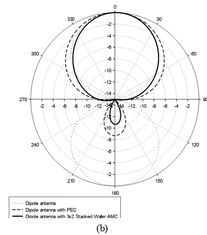
The simulated wafer AMC structure exhibit 90˚ and -90˚ at 910 MHz and 925 MHz of reflection phase respectively. Wafer AMC had overcome the problem of larger AMC size but its bandwidth is slightly smaller than the square patch AMC. In order to increase the bandwidth, the inductivity of the cell must be decreased. From equation (3) the inductance,
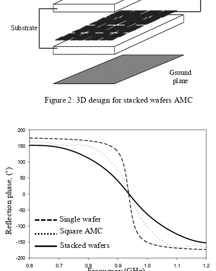
L can be decreased by increasing the thickness, h of the substrate. So, another layer of wafer AMC is stacked at the back of substrate to increase the thickness of the AMC. Figure 2 shows the 3D view of stacked wafers AMC which consist of one ground plane and 2 two pairs of substrate and wafer structure. Using equation (4) the stacked wafers AMC increase the bandwidth of 1.7% to 3.5%. Figure 3 shows the reflection phase of these three different structures; square patch, wafer AMC and stacked wafer AMC.
(4)
Where
fu = upper frequency , fl = lower frequency, fr = resonant frequency
Figure 4 shows the stacked wafers AMC has relatively high surface impedance at the operation frequency of 920 MHz which explain the behavior of the AMC.
Figure 2: 3D design for stacked wafers AMC
0.6 0.7 0.8 0.9 1.0 1.1 1.2
Figure 3: Reflection phase of square patch, wafer and stacked wafers AMC
0.6 0.7 0.8 0.9 1.0 1.1 1.2
Figure 4: Surface Impedance of stacked wafers AMC
IV. TRIPLE-BAND PRINTED DIPOLE ANTENNA WITH OPTIMIZED STACKED WAFERS AMC
Figure 5: 3x2 stacked wafers AMC attach to triple-band meandered dipole value form in one straight line which is approximately at 0 dB. This means that the dipole tag failed to function. Then, by existence of 3x2 stacked wafers AMC helps to reduce the back lobe of the antenna. Hence, it will increase the directivity of the antenna by increasing the major lobe. Table 2 shows the summarization of simulation result for those three cases.
Frequency (GHz) Dipole antenna and stacked w aferAMC
(a)
Dipole antenna with 3x2 Stacked Wafer AMC
(b)
Figure 6: Simulation result (a) return loss (b) radiation pattern of dipole antenna, dipole antenna with PEC and dipole antenna with stacked wafer
AMC.
TABLE 2: COMPARISON BETWEEN DIPOLE ANTENNA, DIPOLE ANTENNA WITH PEC AND DIPOLE ANTENNA WITH STACKED
(b)
(c)
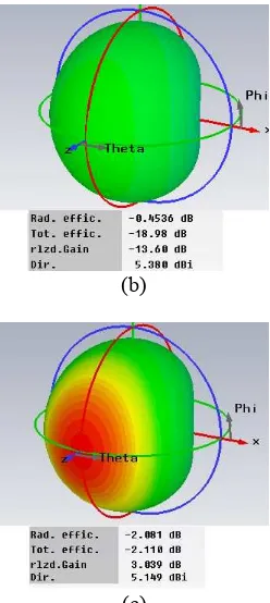
Figure 7: 3D result of gain and directivity of (a) dipole antenna, (b) dipole antenna and PEC (c) dipole antenna with stacked wafers AMC
Figure 7 shows the 3D result of gain and directivity of the meandered dipole antenna, meandered dipole antenna with PEC and meandered dipole antenna with stacked wafers AMC. From Figure 7(b), when meandered dipole antenna is placed on the PEC element, the directivity is increased (5.38 dBi) but the value of gain is slightly decrease which means that the meandered dipole antenna cannot operated when attached to metal based object. When stacked wafers AMC is placed between the antenna and PEC, the value of directivity and gain is increased.
V. CONCLUSION
In this paper, the characteristic of AMC is studied. From the Figure 5 the comparison between basic square patch AMC and stacked wafers AMC is shown. By using the same substrate and simulation setup, the stacked wafers shows higher bandwidth improvement and smaller size. This is because of the different size of slot introduced into the stacked wafers AMC which can help to reduce frequency without increasing the size of the metal patch of the AMC. The optimized 3x1 stacked wafers AMC is proven to improve the directivity, gain and efficiency of the RFID tag antenna when placed onto metal object. The directivity of the antenna with stacked wafers AMC is increased because of the characteristics of the AMC that can help to increase the gain of the main lobe of the radiation pattern. The reading distance of the RFID tag also will be increased when using AMC as a ground plane. Different size of metal object will give different reading range measurement [14] but this will not be discussed in this paper.
ACKNOWLEDGEMENT
This work had been supported by Centre of Research and Innovation Management by Universiti Teknikal Malaysia Melaka under research grant PJP/2012/FKEKK (27B) S1030.
REFERENCES
[1] Zhi Ning Chen and Xianming Qing, “Antennas for RFID Application”, Antenna Technology International Workshop (iWAT) 2010, pp. 1-4. [2] M. E. de Cos, F. Las Heras,Senior Member, IEEE and M. Franco,
“Design of Planar Artificial Magnetic Conductor Ground Plane Using Frequency Selective Surface for Frequencies below 1GHz,” IEEE Antenna and Wireless Propagation Letter, Vol 8, pp. 951-954, 2009.
[3] Dunbao Yan, Qiang Gao and Naichang Yuan, “Strip-Type AMC
Structure and Analysis to Its Band-Gap Characteristics” Progress in Elecromagnetics Symposium 2005,pp. 505-509, Aug 2005.
[4] E. Carrubba, A, Monorchio, and G. Manara “Artificial Magnetic Surface
for Circular Polarization Movemenent” Microwave and Optical
Technology Letters, Vol 5, pp.1782-1786, Aug 2010.
[5] M Elena de Cos, Yuri Alvarez and Fernando Las-HEras, “Design and Characteristics of Planar Artificial Magnetic Conductor in the RFID
SHF Band” Proceeding of Forth European Conference on Antenna and
Propagation 2010, pp. 1-5, Apr 2010.
[6] D. Sievenpiper, L. Zhang Romulo F. Jimenez Boraz, N. G. Alexopolus
and Eli Yablonovitch, “High-Impedance Electromagnetic Surface with a
Forbidden Frequency Band,” IEEE Trans. Microwave Theory and Tech.,
vol. 47, pp. 2059-2074, Nov 1999.
[7] Sievenpiper D.F. “High-Impedance Electromagnetic Surface”, PhD
Thesis, University of California at Los Angeles,1999
[8] Y.Liu,K.M.Luk,H.C.Yin “A RFID Tag Metal Antenna on A Compact
HIS Substrate” PIER pp.51-59, 2010
[9] H.Ayad, M.Fadlallah, H.Youssef "Performance of Low Profile Dipole Antenna AMC-Based Surface Using Metamaterials Structure" 19thInternational Conference in Telecommunication, pp. 987-991, May 2012
[10] P. Raumonen, L. Sydänheimo, L. Ukkonen, M. Keskilammi, and M.
Kivikoski, “Folded dipole antenna near metal plate,” in Proc. IEEE An-
tennas and Propagation Society Int. Symp., vol. 1, Columbus, OH, 2003, pp. 848–851,2003.
[11] L. Ukkonen, M. Soini, D. Engels, L. Sydänheimo, and M. Kivikoski,
“Effect of conductive material in objects on identification with passive
RFID technology: a case study of cigarette cartons,” in Proc. 5th Int. Conf. Machine Automation, Osaka, Japan, 2004, pp. 569–572, 2004.
[12] L. Ukkonen, L. Sydänheimo, and M. Kivikoski, “A novel tag design
using inverted-F antenna for radio frequency identification of metallic
objects,” in Proc. IEEE Sarnoff Symp. Advances Wired and Wireless
Communication, Princeton, NJ, 2004, pp. 91–94,2004
[13] Maisarah Abu, Mohamad Kamal A. Rahim, O. Ayob and F. Zubir,
“Triple-band Printed Dipole Antenna with Single-band AMC-HIS”,
Progress in Electromagnetic Research B. Pier B 20, page 225-244, 2010.
[14] L. Ukkonen, L. Sydänheimo, and M. Kivikoski, “Effect of Metallic Plate
Size on the Performance of Microstrip Patch-Type Tag Antenna for
Passive RFID”, IEEE Antennas and Wireless Propagation Letters, Vol.4,
pp.410-413, 2005.