3D Integration in VLSI
Circuits
Series Editor
Krzysztof Iniewski
3D Integration in VLSI Circuits
Implementation Technologies and Applications Katsuyuki Sakuma
Low Power Semiconductor Devices and Processes for Emerging Applications in Communications, Computing, and Sensing
Sumeet Walia and Krzysztof Iniewski
Biomaterials and Immune Response
Complications, Mechanisms and Immunomodulation Nihal Engin Vrana
Low Power Circuits for Emerging Applications in Communications, Computing, and Sensing
Krzysztof Iniewski and Fei Yuan
High-Speed and Lower Power Technologies
Electronics and Photonics Jung Han Choi and Krzysztof Iniewski
X-Ray Diffraction Imaging
Technology and Applications Joel Greenberg and Krzysztof Iniewski
Compressed Sensing for Engineers
Angshul Majumdar
IoT and Low-Power Wireless: Circuits, Architectures, and Techniques
Christopher Siu and Krzysztof Iniewski
Sensors for Diagnostics and Monitoring
Kevin Yallup and Laura Basiricò
Energy Efficient Computing: Devices, Circuits, and Systems
Santosh K. Kurinec and Sumeet Walia
Radio Frequency Integrated Circuit Design
Sebastian Magierowski
For more information about this series, please visit: https://www. crcpress.com/Devices-Circuits-and-Systems/
book-series/CRCDEVCIRSYS
3D Integration in VLSI
Circuits
Implementation Technologies
and Applications
Edited by
Katsuyuki Sakuma
Managing Editor
Krzysztof Iniewski
Boca Raton, FL 33487-2742
© 2018 by Taylor & Francis Group, LLC
CRC Press is an imprint of Taylor & Francis Group, an Informa business
No claim to original U.S. Government works
Printed on acid-free paper
International Standard Book Number-13: 978-1-1387-1039-9 (Hardback)
This book contains information obtained from authentic and highly regarded sources. Reasonable efforts have been made to publish reliable data and information, but the author and publisher cannot assume responsibility for the validity of all materials or the consequences of their use. The authors and publishers have attempted to trace the copyright holders of all material reproduced in this publication and apologize to copyright holders if permission to publish in this form has not been obtained. If any copyright material has not been acknowledged please write and let us know so we may rectify in any future reprint.
Except as permitted under U.S. Copyright Law, no part of this book may be reprinted, reproduced, transmitted, or utilized in any form by any electronic, mechanical, or other means, now known or hereafter invented, including photocopying, microfilming, and recording, or in any information storage or retrieval system, without written permission from the publishers.
For permission to photocopy or use material electronically from this work, please access www.copyright. com (http://www.copyright.com/) or contact the Copyright Clearance Center, Inc. (CCC), 222 Rosewood Drive, Danvers, MA 01923, 978-750-8400. CCC is a not-for-profit organization that provides licenses and registration for a variety of users. For organizations that have been granted a photocopy license by the CCC, a separate system of payment has been arranged.
Trademark Notice: Product or corporate names may be trademarks or registered trademarks, and are used only for identification and explanation without intent to infringe.
Library of Congress Cataloging-in-Publication Data
Names: Sakuma, Katsuyuki, author.
Title: 3D integration in VLSI circuits : implementation technologies and applications / [edited by] Katsuyuki Sakuma.
Description: Boca Raton, FL : CRC Press/Taylor & Francis Group, 2018. | Series: Devices, circuits, & systems | Includes bibliographical references and index.
Identifiers: LCCN 2018010530| ISBN 9781138710399 (hardback : acid-free paper) | ISBN 9781315200699 (ebook)
Subjects: LCSH: Three-dimensional integrated circuits. | Integrated circuits--Very large scale integration.
Classification: LCC TK7874.893 .A16 2018 | DDC 621.39/5--dc23 LC record available at https://lccn.loc.gov/2018010530
Visit the Taylor & Francis Web site at http://www.taylorandfrancis.com
and the CRC Press Web site at http://www.crcpress.com
v
Contents
Preface ...vii
Series Editor ...xi
Editor...xiii
Contributors ...xv
1. Three-Dimensional Integration: Technology and Design ...1
P. Franzon 2. Three-Dimensional System-in-Package for Application-Specific Integrated Circuit and Three-Dimensional Dynamic Random-Access Memory Integration ...15
Li Li 3. A New Class of High-Capacity, Resource-Rich Field-Programmable Gate Arrays Enabled by Three- Dimensional Integration Chip-Stacked Silicon Interconnect Technology ...41
Suresh Ramalingam, Henley Liu, Myongseob Kim, Boon Ang, Woon-Seong Kwon, Tom Lee, Susan Wu, Jonathan Chang, Ephrem Wu, Xin Wu, and Liam Madden 4. Challenges in 3D Integration ...71
M. Koyanagi, T. Fukushima, and T. Tanaka 5. Wafer-Level Three-Dimensional Integration Using Bumpless Interconnects and Ultrathinning ...85
Takayuki Ohba 6. Three-Dimensional Integration Stacking Technologies for High-Volume Manufacturing by Use of Wafer-Level Oxide-Bonding Integration ...117 Spyridon Skordas, Katsuyuki Sakuma, Kevin Winstel, and
7. Toward Three-Dimensional High Density ...145 S. Cheramy, A. Jouve, C. Fenouillet-Beranger, P. Vivet, and
L. Di Cioccio
8. Novel Platforms and Applications Using Three-Dimensional
and Heterogeneous Integration Technologies ...185 Kuan-Neng Chen, Ting-Yang Yu, Yu-Chen Hu, and Cheng-Hsien Lu
vii
Preface
More and more products are using three-dimensional (3D) integration technology nowadays. Through-silicon vias (TSVs) have been used in high bandwidth memory (HBM) modules and will become mainstream for other high-end products such as graphics processing units (GPU) and high- performance computing (HPC), with applications in databases, security, computational biology, molecular dynamics, deep learning, and automotive. There is no doubt that 3D integration is gaining a significant attention as a promising means to improve performance as it can provide higher intercon-nect speeds, greater bandwidth, increased functionality, higher capacity, and lower power dissipation.
Currently, the term 3D integration includes a wide variety of different integration methods, such as 2.5-dimensional (2.5D) interposer-based inte-gration, 3D-integrated circuits (3DICs), 3D systems-in-package (SiP), 3D het-erogeneous integration, and monolithic 3D ICs. The goal of this book is to provide readers with an understanding of the latest challenges and issues in 3D integration. TSVs are not the only technology element needed for 3D integration. There are numerous other key enabling technologies required for 3D integration and the speed of the development in this emerging field is very rapid. To provide readers with state-of-the-art information on 3D integration research and technology developments, each chapter has been contributed by some of the world’s leading scientists and experts from aca-demia, research institutes, and industry from around the globe.
Chapter 1 by Prof. Franzon from North Carolina State University
(NCSU) provides a brief review of 2.5D and 3D technology options, including interposers and TSV-stacking technologies. As illustrated by successful commercial 3D products and experimental results of complemen-tary metal–oxide–semiconductor (CMOS) stacks with a copper thermo- compression-bonded interface, Chapter 1 discusses the reasons why 3D integration is superior in terms of power efficiency, performance enhance-ment, and cost reduction.
Chapter 2 by Dr. Li from Cisco Systems describes up-to-date
Chapter 3 presents architecture, design, and technology implementations for 3D field-programmable gate array (FPGA) integration and was written by Dr. Ramalingam et al. from Xilinx, one of the major players in this area. Multiple FPGA dies are placed side by side and interconnected on a large silicon interposer. The design simulation methodology, reliability assess-ment, and future challenges are discussed. On these topics, the authors provide an industry perspective based on volume production of the largest 3D-integrated FPGA as of today, which contains 4.4 million logic cells, 600 thousand microbumps, and 19 billion transistors in a 55 mm package.
Chapter 4 by Prof. Koyanagi et al. from Tohoku University, Japan, covers
various unique 3D system-on-chips technologies, such as 3D integration using self-assembly and electrostatic bonding, TSV formation based on directed self-assembly with nanocomposites, and hybrid bonding technol-ogy using Cu nano-pillar. Technologies for a 3D-integrated CMOS image sensor module for a driver assistance system are presented, and future 3D integration challenges are also discussed.
Chapters 5 and 6 focus on fabrication approaches for 300 mm wafer-level
3D integration without microbumps. For high-volume manufacturing, TSVs are formed after a wafer-bonding process. The leakage current and electrical resistance of TSVs, Ion/Ioff characteristics for field-effect transistor
(FET) devices, and the characteristics of wafer-bonding technologies are also discussed. Chapter 5 by Prof. Ohba from the Tokyo Institute of Technology, Japan, deals with the 3D integrations of permanently adhesive-bonded ultra-thin wafers. In Chapter 6, Dr. Skordas et al. from IBM discussed the 3D inte-gration technology based on low-temperature oxide-bonding for integrating high-performance POWER7™ 45 nm silicon-on-insulator (SOI)-embedded DRAM.
Chapter 7 by Ms. Cheramy et al. from CEA-Leti, France, provides the
principles, process integration, and detailed overviews of both monolithic 3D ICs (CoolCube™) and Cu/SiO2 hybrid bonding technologies. Monolithic
3D ICs enable the stacking of multiple transistor layers in the third dimension, with a vertical interconnect pitch in the range of a few tens of nanometers, and the bottom layer can be any CMOS type, be it bulk planar FET, FinFET, or fully-depleted silicon-on-insulator (FDSOI). Potentially, it will be a key technology driver for the next generation of 3D integration. The Cu/SiO2
hybrid bonding technology enables wafer-to-wafer and die-to-wafer connec-tivity with a vertical interconnect pitch in the range of a few micrometers. This chapter also addresses the issue of thermal dissipation in 3D integration.
Chapter 8 by Prof. Chen et al. from National Chiao Tung University, Taiwan,
ix
Preface
I would like to sincerely thank all of the authors for their hard work and commitment. Without their contributions, it would not have been possible to provide an up-to-date review of these innovative technologies and the chal-lenges in 3D integration. It is my hope that this book will provide readers with a timely and comprehensive view of current 3D integration technology.
xi
Series Editor
Krzysztof (Kris) Iniewski is managing R&D at
xiii
Editor
Katsuyuki Sakuma is a research staff member
at the IBM T.J. Watson Research Center. He has over 19 years of experience of researching 3D integration technologies and performing various semiconductor packaging research and development projects. His research interests include 3D integration technologies, bonding technologies, advanced packaging, and bio-medical sensors.
He has published more than 85 peer-reviewed journal papers and conference proceeding papers, including three book chapters in the semiconductor and electronic packaging area. He also holds over 35 issued or pending U.S. and international patents. He has been recognized with the IBM Eleventh Invention Achievement Award in 2017 and an Outstanding Technical Achievement Award (OTAA) in 2015 for his contribution and leadership in the area of 3D integration technology development. He was also given the 2018 Exceptional Technical Achievement Award from the IEEE Electronics Packaging Society, and the 2017 Alumni Achievement Award from his Alma Mater, the School of Engineering at Tohoku University, for his contribution to 3D chip stack tech-nology development in the electronics packaging industry. He was a core-cipient of the IEEE Components, Packaging, and Manufacturing Technology (CPMT) Japan Society Best Presentation Award in 2012, and the IMAPS “Best of Track” Outstanding Paper Award in 2015.
xv
Department of Electronics Engineering
National Chiao Tung University Hsinchu City, Taiwan
North Carolina State University Raleigh, North Carolina
T. Fukushima
Department of Mechanical Systems Engineering
Tohoku University Sendai, Japan
Yu-Chen Hu
Department of Electronics Engineering
National Chiao Tung University Hsinchu City, Taiwan
IBM T.J. Watson Research Center Yorktown Heights
Albany, New York
M. Koyanagi
Li Li
Department of Electronics Engineering
National Chiao Tung University Hsinchu City, Taiwan
Liam Madden
Xilinx, Inc.
San Jose, California
Takayuki Ohba
Laboratory for Future
Interdisciplinary Research of Science and Technology Tokyo Institute of Technology Tokyo, Japan
Suresh Ramalingam
Xilinx, Inc.
San Jose, California
Katsuyuki Sakuma
IBM T.J. Watson Research Center Yorktown Heights
Department of Biomedical Engineering
Department of Electronics Engineering
1
1
Three-Dimensional Integration:
Technology and Design
P. Franzon
1.1 Introduction
3D and 2.5D integration technologies permit substantial improvement in form factor, power, performance, functionality, and sometimes even cost. Though not providing a direct replacement for Moore’s law, 3D technologies can permit a generation or more of exponential scaling in power per unit of performance and other factors.
This chapter is structured as follows. First there is a review of 3D technolo-gies, followed by a general discussion of commercial 3D success stories and technology drivers. Included in that we review 3D logic projects conducted at North Carolina State University, United States, before closing out on het-erogeneous integration.
CONTENTS
1.1 Introduction ...1
1.2 Three-Dimensional Integrated Circuit Technology Set ...2
1.3 Three-Dimensional Drivers...5
1.4 Miniaturization ...5
1.5 Cost Reduction ...6
1.6 Heterogeneous Integration ...7
1.7 Performance Enhancement ...8
1.8 Power Efficiency ...10
1.9 Conclusion ...12
1.2 Three-Dimensional Integrated Circuit Technology Set
There are a variety of technologies that contribute to the 3D technology set. The purpose of this chapter is to review these technologies and not to pro-vide details of materials and manufacturing options. We will review inter-posers, 3D stacking technologies and monolithic 3D technologies.
Figure 1.1 shows an interposer, often referred as a multi-chip module in
the past. Interposers get its name from their functionality of being placed between the chip and the package. There are two standard ways to make interposers. One approach is to use multiple thin film layers of spun-on dielectrics and metal patterning. While permitting thick metals, it does not permit high density. High density can be achieved by leveraging a legacy back-end-of-line (BEOL) process from semiconductor chip manufacturing. A BEOL process permits multiple levels of planarized wiring, typically 4–6 layers.
A defining technology in 3D integration is the through-silicon via (TSV). The
TSV goes through the silicon substrate, connecting the front and back sides of the structure. It is created by etching a near vertical hole, lining it with a dielectric before filling it with metal. The wafer is then thinned to expose the metal. Typical dimensions for interposer structures are 100 μm of
thick-ness for the overall structure and 1–10 μm width and space for the metals.
TSVs are typically on at least a 100 μm pitch. The microbumps are typically
around a 40 μm pitch, whereas the bumps to the package must be on
conven-tional scales at 150+ μm pitch.
Figure 1.2 provides an illustration for some of the key three-dimensional
integrated circuit (3DIC) stacking technologies. This shows a three-chip stack, two of which incorporate TSVs. The top two chips are joined with a face-to-face technology (F2F). Here face refers to the top side of the chip—
where the transistors and interconnect are. Several methods are used to cre-ate high-density F2F connections. Microsolder bumps can be used but today
Interposer Microbump
Wiring layers Through-silicon vias (TSVs) Bumps
Oxide Silicon
FIGURE 1.1
3
3D Integration: Technology and Design
they are limited to 40 μm pitch (with potential for 25 μm). Copper–copper
thermo-compression can be used down to sub-5 μm pitches. Alternatively,
hybrid bonding can be used. In hybrid bonding the top surface, with metal plugs in it, is planarized and then bonded to another such surface. An exam-ple is the Ziptronix data-based individualization (DBI) process [1]. This pitch can be built down to 1 μm pitch but 6–8 μm are more typical. Hybrid
bond-ing is used to make many cell phone cameras today (Please see Section 1.6
on heterogeneous integration). With such high interconnect densities, many interesting architectures can be explored, as will be explained later.
The bottom two chips in Figure 1.2 are joined using a face-to-back (F2B) arrangement in which the bottom (back) of one die is joined to the top (face) of
another. TSVs are needed to provide the connection to the joining backside. As the sidewalls of the TSV are not entirely vertical, the TSV pitch is limited to approximately the thickness of the wafer, typically 10–25 μm. Thus a F2B
connection provides a lot of less density than a F2F connection.
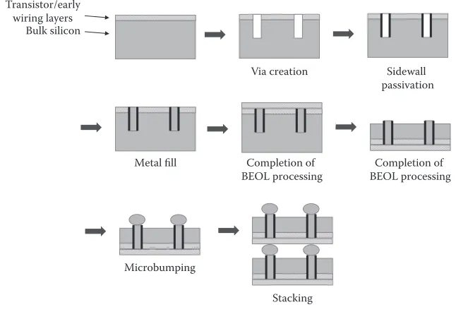
TSVs can be inserted before, during, or after complete wafer processing. These are referred to, respectively, as via early, middle, and last. Figure 1.3
shows a process via middle. Wafers are partially completed, say to metal 1. A vertical side-wall via is etched part way through the wafer. This via is created using the Bosch process [2]. In the Bosch process, deep reactive-ion etching (DRIE) is alternated with a deposition step multiple times to cre-ate a near vertical wall via. Today the wall steepness is typically 10:1. Thus the via depth has to be less than 10× the diameter of the opening at the
top. The via sidewalls are passivated, typically with an oxide, and then filled with a metal, typically tungsten or copper. The chip metal stack (BEOL) is then completed. The wafers are then flipped and thinned, exposing the TSV metal. The exposed metal can then be used directly for a joining process, or a bump structure is added before joining with another wafer or chip to create a 3D stack.
Microbumps or direct bond Transistor/wiring layers Through-silicon vias (TSVs) Microbumps to package or interposer
FIGURE 1.2
Note in Figure 1.2 that the top chip has not been thinned. Usually a 3D chip stack is assembled with the chip in wafer form. Two wafers are attached with the second left unthinned. This wafer stack can be attached to another (thick) wafer for further handling. In most cases, one wafer is left in a thick format so that the wafer stack can be easily handled. Thin wafer handling is possible but increases the cost.
Most 3DICs are assembled in wafer format. Again, the driver is cost. Wafer-to-wafer attachment processing costs less per die and has higher yields. Although chip to wafer attachment is possible it is not widely used.
An intriguing complement to 3D chip stacking technology is monolithic 3D in which there is only one silicon substrate (and thus no TSVs). The most commercially successful one of these technologies is 3D NAND Flash in which the string of NAND transistors in a nonvolatile flash device is fabri-cated vertically. This approach brings substantial density improvements and cost savings over conventional NAND flash technology. However, to date it has not been commercially applied to any other logic or memory structure.
Another monolithic (-like) 3D technology set involves techniques in which silicon-on-insulator (SOI) wafers are the starting wafer. This is shown in
Figure 1.4. In this approach, fabricated wafers are joined face to face using an oxide–oxide bond. As the transistors are built on the top of an oxide layer, a silicon-selective back etch can be used to remove the silicon part of the SOI substrate while not affecting the transistors and interconnect layers. Simple
Transistor/early wiring layers
Bulk silicon
Via creation Sidewall
passivation
Metal fill Completion of BEOL processing
Completion of BEOL processing
Microbumping
Stacking
FIGURE 1.3
5
3D Integration: Technology and Design
through-oxide vias can then be used to create vertical connections between what were previously separate chips. An example of this process can be found in Reference 3. If the first two chips in the stack are fabricated without interconnect, then one gets two directly connectable transistor layers in what would be considered a monolithic 3D technology. This is monolithic in the sense there is only one bulk wafer left at the end of processing. However, many would not consider it to be truly monolithic as multiple separate wafers have to be created first.
1.3 Three-Dimensional Drivers
In general, the decision to employ 3D technologies is driven by (1) the need for miniaturization, (2) the desire for cost reduction, (3) heterogeneous inte-gration, (4) the need for performance enhancement, and/or (5) the need for improvement in performance/power. Often several of these go hand in hand.
1.4 Miniaturization
An early application of TSVs was providing the I/O connections cell phone camera front-side imaging sensor [4,5]. The goal was not to leverage 3D chip stacks—these were single die—but to reduce the overall sensor height, at least when compared with conventional packaging approaches.
Metal transistors
BEOL oxide Epi Buried oxide Bulk silicon
1. Oxide–oxide bond 2. Silicon etch 3. Via formation
4. Repeat
FIGURE 1.4
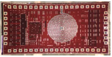
3D chip stacking can be used to make such sensors with low integrated volume. Though fabricated using wire bonding, Chen et al. demonstrated an integrated power-harvesting data-collecting sensor with the photovoltaic power-harvesting chip mounted on top of the logic and RF chips [6]. This maximizes the photovoltaic power-harvesting area while minimizing the volume. TSVs and bonding technologies would permit further volume reduc-tion. Lentiro [7] described a two-chip stack aimed at simulating a particle of meat for the purposes of calibrating a new food processing system. One chip is a radio-frequency identification (RFID) power harvester and communica-tions chip, the second is the temperature data logger. It is a two-chip stack with F2F connections and TSV-enabled I/O. It is integrated with a small bat-tery for data collection purposes only as the RFID cannot be employed in the actual processing pipes. The two-chip stack permits smaller imitation food particles than otherwise would be the case and is shown in Figure 1.5. The RFID coil can be seen. The chip includes capacitors for temporary power storage.
1.5 Cost Reduction
There have been several examples of 3DIC products with a focus on cost reduction, though often they achieve performance enhancement simultaneously.
Many cell phone cameras are today made as a two-chip stack. One chip is a backside-illuminated pixel array that does not include interconnect layers or even complete complementary metal–oxide–semiconductor (CMOS) transis-tors. The second chip is a complete CMOS chip on which the analog-to-digital converters (ADC) are built and interconnected for all other functionalities required of an image sensor. A high-density connection process such as hybrid bonding is used to create the needed face-to-face connections on a
FIGURE 1.5
7
3D Integration: Technology and Design
few micron pitch. Examples are reported in References 8 and 9. This is also an example of heterogeneous integration, as the two chips in the stack go through different manufacturing processes.
Another example of cost reduction is found in building high-end field-programmable gate arrays (FPGAs). To a first approximation, the cost of a large CMOS chip goes up with the square of the area. This is because the probability of a defect occurring on the chip and thus killing the chip
goes up with the chip area, whereas the cost of making the chip in the first place also goes up with the area. Thus it is worth considering partitioning a large chip into a set of smaller ones, if the cost of integration and the addi-tional test are less than the savings accrued to increase CMOS yield. Xilinx, California, United States, investigated this concept for large FPGAs and is now selling FPGA modules containing 2–4 CMOS FPGA chips, tightly inte-grated on an interposer. Details are not available but they claim an overall cost savings [10].
A third example is that of mixing technology nodes. In general, Moore’s law tells us that a digital logic gate costs less to make in a more advanced technology due to the reduced area for that gate in that node. However, in contrast, many analog and analog-like functions such as ADC and high-speed serial deserializer I/Os (SerDes) do not benefit in such a fashion. The reason is that the analog behavior of a transistor has higher variation for smaller transistors than for larger ones. Thus for many analog functions that rely on well-matched behaviors of different transistors in the circuit, no ben-efit is accrued from building smaller transistors. More simply put, analog circuit blocks do not shrink in dimensions with the use of more advanced technologies. Thus the cost of these functions in a more advanced process node can actually be higher, than in the old node, as the old node costs less to make per unit of area. Again this is an example of heterogeneous integration, the heterogeneity being that of mixing technology notes.
Although Wu [10] also explored this concept generically, Erdmann et al. [11] have explored this concretely for a mixed ADC/FPGA design. Their design consisted of two 28 nm FPGA logic dies, integrated with two 65 nm ADC array dies on an interposer. Thus two sets of cost benefits are accrued, first the yield-related savings from splitting the logic die into two and the fabrication cost savings of keeping the ADCs in an older technology.
1.6 Heterogeneous Integration
In Section 1.5, two examples of heterogeneous integration were given in
Another interesting use of 3D technologies has been to build nonvisible light sensors, sometimes using a nonsilicon technology for the sensing layer. Examples include IR imagers, X-ray imagers [12], and other images for high-energy physics investigations [13].
The example is that of mixing III-V and silicon technologies. This is best exemplified by The Defense Advanced Research Projects Agency Diverse Accessible Heterogeneous Integration (DARPA DAHI) program in which GaN and InP chips are integrated on top of the CMOS chips through micro-bumps and other technologies [14]. More specifically, CMOS can be used for most of the transistors in a circuit, whereas GaN high-electron-mobility transistors (HEMTs) can be used for its high-power capability, and InP het-erojunction bipolar transistors (HBTs) can be used for their very high speed. An example of the latter is an ADC. In an ADC, only a few transistors gen-erally determine the sampling rate. Thus with the DAHI technology, these few transistors can be built in a high speed, but expensive and low yielding, InP chiplet, whereas the rest of the ADC is built in cheaper and more robust CMOS.
1.7 Performance Enhancement
A major goal of using 3D technologies is to increase the performance in some key aspects. For example, a two-layer image sensor might enable bigger pix-els in the image layer and thus greater sensitivity. Alternatively, integrating a high-performance low device count InP chiplet onto a sophisticated CMOS die leads to performance improvement, often in conjunction with the high I/O count that the 3D technologies permit.
However, many 3D products and research objects are driven purely by performance, specifically the ability to integrate many silicon parts, with a lot of accumulated area into one 3D chip stack.
9
3D Integration: Technology and Design
There have been several proposed 3D memory technologies, which are summarized together with 2D memories in Table 1.1. Note that in this table, both B (Byte) and b (bits) are used. Also note that 1 mW/Gb/s is equivalent to 1 pJ/bit.
The Hybrid Memory Cube (HMC) is a joint Intel-Micron standard that cen-ters on a 3D-stacked part including a logic layer and multiple DRAM layers organized as independent vertical slices. This 3D chip stack is then provided as a packaged part, so the customer does not have to deal with any 3DIC or 2.5D packaging issues. At the time of writing this chapter, Micron offered 2 GB and 4 GB parts with a maximum memory bandwidth of up to 160 GBps (The 128 GBps part is used in Table 1.2). The data I/O is organized as an eight high-speed serial channels or lanes. HMC is mainly aimed at computing applications. However, it does not appear to be widely adopted.
The high bandwidth memory (HBM) is a JEDEC (i.e., industry) stan-dard that is not intended to be packaged on its own but to be further inte-grated using an interposer or 3D chip stack. Its high pin count, configuring 8 × 128-bit wide interfaces, prevents it from being packaged easily. The
inter-faces run at 2 Gbps per pin and the pins are placed on a dense 48 × 55 μm
grid. It is fabricated as a stack of multibank memory die, connected to a logic
TABLE 1.1
Comparison of 2D and 3D Memories
Technology Capacity BW (GB/s)
Power
DDR4-2667 4 GB 21.34 6.6 309 6.5–39 32
LPDDR4 4 GB Up to 42 5.46 130 2.3 32
HMC 4 GB 128 GBps 11.08 86.5 10.8 8 Serdes
lanes
HBM 16 GB 256 GBps 48 1024
Wide I/O 8–32 GB 51.2 GBpsa 42b 256
DiRAM4 64 GB 8 Tbps 4096
a Wide I/O2, Wide I/O1 was half of this. b Wide I/O1, Wide I/O2 should be lower.
TABLE 1.2
Improvements in 3D Design over 2D Using Logic Cell Partitioning
die through a TSV array, the TSV arrays running through the chip centers. Each chip is F2B mounted to the chip beneath it. The eight channels are oper-ated independently. Details for a first-generation HBM (operating at 3.8 pJ/bit power level at 128 GB/s) can be found in Reference 15. The use of HBM in graphics module products has been announced by Nvidia and AMD.
Wide I/O is also a JEDEC-supported standard, aimed largely at low-power mobile processors. Although intended to be mounted on top of the logic die in a true 3D stack, side by integration on an interposer is also possible. Wide I/O is a DRAM-only stack—there is no logic layer. Instead the DRAM stack is exposed through a TSV-based interface and the memory controller is designed separately on the CPU/logic die that is customer designed. To date the thermal challenges of mounting a DRAM on an already hot mobile processor logic die have been insurmountable, especially as it is desired to operate the DRAM at a lower temperature than logic (85°C for DRAM vs.
105°C for logic) to control leakage and refresh time. This has been a barrier
to adoption.
The Tezzaron DiRAM4 is a proprietary memory still in development. It has 4096 data I/O organized across 64 ports. It is intended only for 3D and interposer integration. It has a unique organization in that the logic layer is not only used for controller and I/O functions but also houses the global sense amplifiers and addresses decoders that in other 3D memories are on the DRAM layers. This permits faster operation for these circuits. The DiRAM4 has potential for a very high bandwidth (up to 8 Tbps) and fast random cycles (15 ns) [16].
1.8 Power Efficiency
In theory, taking a 2D chip and turning it into a stack of two chips should reduce the power of the chip by about 35%. The reason is quite simple. In
most digital chips, about half (50%) the power is consumed in driving wires.
When stacked, the two chips in the stack should be half of the area of the original chip, and thus the wires should be √2 shorter. As the power needed to drive a wire is roughly proportional to its length, each wire driver should see a power reduction of around 70%, that is, the chip as a whole should see
a power reduction of around 35%.
However, this is difficult to achieve as short wires are unlikely to be routed between the two chips. On the other hand, reduced wire loads also means the chip can operate faster. Thus one would still expect to see a substantial improvement in the power/performance ratio over the 2D equivalent.
11
3D Integration: Technology and Design
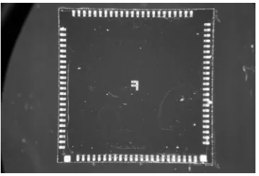
a CAD flow to do this that could reuse 2D CAD tools, especially place and route tools. To make that feasible, all flip-flops are kept in one tier so that 3D clock distribution was not required. The radar PE was implemented in the Tezzaron bulk CMOS 3D process [17] (Figure 1.6). The results are summa-rized in Table 1.2. On average, performance per unit of power was increased by 22% due to the decreases in wire length achieved through this
parti-tioning approach. The radar processor had an improvement in performance per unit of power of 21%. The other designs achieved 18% and 35%. The
achieved improvement was roughly equivalent to one generation of Moore’s law scaling.
In a different project at North Carolina State University, we took a very differ-ent approach to improving performance/power using 3D technologies. A stack of two different CPUs are integrated vertically using a vertical thread transfer
bus that permits fast compute load migration from the high-performance CPU to and from the low-power CPU when an energy advantage is found [18]. In this design, the high-performance CPU can issue two instructions per cycle, whereas
the low-power CPU is a single-issue CPU. The transfer is managed using a
low-latency, self-testing multisynchronous bus [19]. The bus can transfer the state of the CPU in one clock cycle by using a wide interface and by exploiting a high-density copper–copper direct bond process. The caches are switched at the same time, removing the need for a cold cache restart.
Simulation with Specmark workloads shows a 25% improvement in the
power/performance ratio compared with executing the sample workload solely in the high-performance processor. In contrast, if the workload was executed solely in the single-issue (low-power) CPU, there would be 28%
total energy savings, compared with keeping the workload in the high- performance CPU but at the expense of a 39% reduction in performance. If
the workload was allowed to switch every 10,000 cycles, there would be 27%
total energy savings but at the expense of only a 7% reduction in performance
that is, a 25% improvement in power per unit of performance is achieved. The
die photograph is shown in Figure 1.7.
Logic only
Logic, clocks,
flip-flops Die photo
1.9 Conclusion
3D and 2.5D technologies considerably open the design space for semicon-ductor technologies. Dimensions for exploration include miniaturization, cost reduction, achieving new modalities via heterogeneous integration, per-formance improvement, and improvement in perper-formance/power.
References
1. P. Enquist, G. Fountain, C. Petteway, A. Hollingsworth, and H. Grady, Low cost of ownership scalable copper direct bond interconnect 3D IC technology for
three dimensional integrated circuit applications, IEEE International Conference
on 3D System Integration, 3DIC 2009, San Francisco, CA, 2009, pp. 1–6.
2. U.S. Patents 5,501,893 and 6,531,068.
3. J.A. Burns, B.F. Aull, C.K. Chen, C. Chang-Lee, C.L. Keast, J.M. Knecht, V. Suntharalingam, K. Warner, P.W. Wyatt, and D. Yost, A wafer-scale 3-D
cir-cuit integration technology, IEEE Transactions on Electron Devices, 52(10): 2507–
2516, 2006.
4. http://image-sensors-world.blogspot.com/2008/09/toshiba-tsv-reverse-engineered.html
5. http://www.semicontaiwan.org/en/sites/semicontaiwan.org/files/docs/ 4._mkt__jerome__yole.pdf
6. G. Chen, M. Fojtik, D. Kim, D. Fick, J. Park, M. Seok, M.-T. Chen, Z. Foo, D. Sylvester, and D. Blaauw, Millimeter-scale nearly perpetual sensor system
with stacked battery and solar cells, 2010 IEEE International Solid-State Circuits
Conference-(ISSCC), San Francisco, CA, 2010, pp. 288–289.
7. A. Lentiro, Low-density, ultralow-power and smart radio frequency telemetry sensor, PhD Dissertation, NCSU, 2013.
FIGURE 1.7
13
3D Integration: Technology and Design
8. P. Enquist, 3D integration applications for low temperature direct bond
tech-nology, 2014 4th IEEE International Workshop on Low Temperature Bonding for 3D
Integration (LTB-3D), Tokyo, Japan, 2014, p. 8.
9. http://www.sony.net/SonyInfo/News/Press/201201/12-009E/index.html, http://www.reuters.com/article/2014/03/25/us-sony-sensors-idUSBREA 2O0PQ20140325
10. X. Wu, 3D-IC technologies and 3D FPGA, 3D Systems Integration Conference
(3DIC), 2015 International, Sendai, Japan, 2015, pp. KN1.1–KN1.4.
11. C. Erdmann et al., A heterogeneous 3D-IC consisting of two 28 nm FPGA die
and 32 reconfigurable high-performance data converters, IEEE Journal of
Solid-State Circuits, 50(1): 258–269, 2015.
12. G.W. Deptuch et al., Fully 3-D integrated pixel detectors for X-rays, IEEE
Transactions on Electron Devices, 63(1): 205–214, 2016.
13. http://meroli.web.cern.ch/meroli/DesignMonoliticDetectorIC.html
14. S. Raman, C.L. Dohrman, and T.H. Chang, The DARPA diverse accessible het-erogeneous integration (DAHI) program: Convergence of compound
semi-conductor devices and silicon-enabled architectures, 2012 IEEE International
Symposium on Radio-Frequency Integration Technology (RFIT), Singapore, 2012,
pp. 1–6.
15. D.U. Lee et al., A 1.2 V 8 Gb 8-channel 128 GB/s high-bandwidth memory
(HBM) stacked DRAM with effective I/O test circuits, IEEE Journal of Solid-State
Circuits, 50(1): 191–203, 2015.
16. www.tezzaron.com and Evolving 2.5D and 3D integration, RTI 3D ASIP, December 2013.
17. T. Thorolfsson, S. Lipa, and P.D. Franzon, A 10.35 mW/GFLOP stacked SAR
DSP unit using fine-grain partitioned 3D integration, Proceedings in Custom
Integrated Circuits Conference 2012, pp. 1–4.
18. E. Rotenberg, B.H. Dwiel, E. Forbes, Z. Zhang, R. Widialaksono, R. Basu Roy Chowdhury, N. Tshibangu, S. Lipa, W.R. Davis, and P.D. Franzon, Rationale for
a 3D heterogeneous multi-core processor, 2013 IEEE 31st International Conference
on Computer Design (ICCD), pp. 154, 168, October 6–9, 2013.
19. Z. Zhang, B. Noia, K. Chakraparthy, and P. Franzon, Face to face bus design
15
2
Three-Dimensional System-in-Package
for Application-Specific Integrated
Circuit
and Three-Dimensional Dynamic
Random-Access Memory Integration
Li Li
2.1 Three-Dimensional SiP Introduction
The bandwidth for high-performance networking switches and rout-ers increases two to ten times for every new generation. This in turn drives the bandwidth requirements for the application-specific integrated circuits (ASICs) and their external memory devices designed for the
CONTENTS
2.1 Three-Dimensional SiP Introduction ...15
2.2 Enabling Technologies for 3D SiP ...17
2.2.1 Three-Dimensional Stackable Memory ...17
2.2.2 High-Density Interposer ...19
2.2.2.1 Silicon Interposer ...19
2.2.2.2 Organic Interposer ...21
2.2.3 Microbump Interconnect ...23
2.3 3D SiP for Application-Specific Integrated Circuits and High
Bandwidth Memory Integration ...25
2.3.1 Organic Interposer Design ...26
2.3.2 Simulation and Results ...27
2.4 Three-Dimensional SiP Assembly ...29
2.5 Test and Characterization ...32
2.6 Reliability Challenge ...33
2.7 Summary ...37
high-performance network systems. To meet these bandwidth require-ments, the ASIC packaging technology has to keep up with the integrated circuit (IC) technology scaling. Recently several 2.5-dimensional (2.5D) and 3-dimensional (3D) IC integration or packaging technology platforms have been developed to address the gap seen between the slowdown of Moore’s law scaling and the ever-increasing system integration requirements. In the remainder of this chapter, the terms 2.5D and 3D IC integration and 2.5D and 3D packaging are used interchangeably.
The early success of FCAMP that stands for Flip Chip and Memory Package provided a much-needed solution to the bandwidth challenges between the ASIC and memory devices designed for a high-end networking application [1]. The FCAMP, sometimes also referred to as a system-in-package (SiP), con-tains an ASIC die that is attached to an organic substrate using the flip chip technology. The memory devices are packaged, tested at-speed and burned-in before puttburned-ing on the SiP substrate. This process flow is compatible to the now industry-standard flip chip assembly process and has achieved high manufacturing yield. The other innovation that made the FCAMP a success is the availability of large size (>52.5 mm), high density, thin-core or
core-less, and high-performance organic substrates that are based on the build-up, micro-via technologies [2]. The bandwidth improvement through the FCAMP design has had a profound impact on high-performance network-ing switches and routers, similar to computnetwork-ing applications.
Leveraging 3D IC integration, a concept of 3D ASIC and memory integra-tion with a silicon interposer and through-silicon via (TSV) was proposed and a feasibility study was conducted [3]. 3D ASIC and memory heteroge-neous integration can be considered as an extension of the FCAMP that was developed about a decade ago. It has the advantages of reducing power con-sumption, improving the bandwidth between the ASIC and memory, and modularizing system hardware designs. Critical components for enabling 3D ASIC and memory integration include large-size silicon interposer, 3D-stacked memory with TSV, and microbump or micropillar interconnects.
17
3D System in Package
Here HBM stands for high bandwidth memory, which is a 3D-stacked dynamic random-access memory (DRAM) device developed by major DRAM suppliers in recent years.
The interposers used in 2.5D or 3D SiP can provide much higher wiring density than the conventional organic build-up substrate. Together with the microbump interconnect technology, the 3D ASIC and memory SiP can greatly increase the width and density of the interface between the ASIC and the memory devices, and hence the bandwidth. The 3D SiP for ASIC and memory integration has the following advantages:
• High package thermal performance similar to the single flip-chip module
• Higher interconnect wiring density than the conventional organic build-up substrate
• Compatible to the flip-chip assembly process
• Lower CTE mismatch between the silicon chips and the interposer • Lower stresses on the low-k dielectrics and interconnects of the
sili-con chips by leveraging the Cu-filled interposer as a stress buffer
2.2 Enabling Technologies for 3D SiP
2.2.1 Three-Dimensional Stackable Memory
In the past several years, memory suppliers started the development of low-power, high-bandwidth, 3D-stackable memory devices. Industry standards for the 3D-stackable memory devices have also been developed. An early
Package substra te Interposer
ASIC HBM
HBM
HBM HBM
FIGURE 2.1
example of 3D IC integration is the application of 3D-stacked (3DS) DRAM with TSV [6]. Published in December 2013, the addendum to JESD79-3 defines the 3DS DDR3 SDRAM specification, including features, functionalities, AC and DC characteristics, packages, and ball/signal assignments. Since then, 3DS DDR3 and 3DS DDR4 have been developed and are now in mass pro-duction to meet the ever-increasing demand in memory module density for server, high-performance computing (HPC) and networking applications. In parallel to the development of 3DS DDR3 and 3DS DDR4, Wide I/O mobile DRAM was developed leveraging the same 3D IC stacking technology. The Wide I/O single date rate (SDR), which is 512-bit wide, running at 200 MHz can provide a total bandwidth of 12.8 GB/s and consumes only half the power of a low-power double data rate (LPDDR2) on the per bandwidth base [7]. The second-generation Wide I/O DRAM, Wide I/O 2, provides four times the memory bandwidth (up to 68 GB/s) of the previous version but at lower power consumption [8]. From a packaging perspective, the Wide I/O DRAM is designed specifically to stack on top of a system-on-chip (SoC) logic device such as an application processor (AP) die using TSVs and microbumps or micropillars to minimize electrical interference and the overall package form factor that is much needed for mobile applications.
Using a similar 3D heterogeneous integration approach, a consortium led by Micron Technology developed the Hybrid Memory Cube (HMC) [9]. The HMC consists of a 3D stack of DRAM dies on top of a logic memory interface/ controller die. The DRAM dies within the stack are each of 1 GB in DRAM density and are divided into 16 partitions. Each partition has two banks (also called arrays), and its own data and control TSVs. HMC is designed to emphasize massive amounts of bandwidth at higher power consumption and cost than Wide I/O 2.
For the 3D ASIC and memory SiP designs, these 3D-stackable memory devices have advantages that include the following:
• Memory and ASIC (logic) device can each be built in their own spe-cific processes.
• Further exploit the process/cost differences between the logic and memory devices.
• Very high data rate (bandwidth) with low latency and low-power per bandwidth.
• Wide interface enabled by very wide interdie interconnect. • Low parasitic enabled by short, direct interconnect.
Recently, this SiP approach has been extended to include the HBM DRAM devices based on 3D IC integration with TSV and micropillar intercon-nects [5].
19
3D System in Package
processor units (GPU), HPC, server, networking, and client applications where peak bandwidth, bandwidth per watt, and capacity per area are valued metrics. The high bandwidth is delivered using a 1024-bit wide memory interface that is divided into eight independent channels. To accommodate the 1024-bit interface between HBM and the host compute die, micropillars with a pitch of 55 microns are placed at the bottom of the HBM DRAM die stack.
2.2.2 High-Density Interposer
2.2.2.1 Silicon Interposer
The introduction of 3D IC integration also brought new requirements and sometimes disruptions to the existing microelectronics manufacturing sup-ply chain. One example is the manufacturing and supsup-ply of silicon interposers (Si-IP). Currently there are three commonly used interposer-manufacturing process flows. The first can be referred to as the Foundry Process flow. The
sili-con interposer is fabricated completely by the wafer foundry and sometimes the service even includes packaging the 3D IC subassembly to the package substrate [11].
The second can be referred to as the middle-end-of-line (MEOL) process flow.
MEOL is often used by the outsourced assembly and test (OSAT) suppli-ers for processing TSV wafsuppli-ers with active circuits. It is usually started at the wafer foundry for via generation and filling, and fabrication of front-side metal wiring layers. Then the full thickness wafers are delivered to the OSAT for further downstream processes that include wafer thinning, TSV reveal, backside metal layer generation, passivation, and bumping. The third process can be called as the substrate process flow. In this case, the silicon
interposer is fabricated and supplied by the traditional packaging substrate suppliers. A comparison of these silicon interposer manufacturing and sup-ply chain flows is given schematically in Figure 2.2.
Front side
Foundry TSV and
FEOL
MEOL process at OSAT
Back side
For both the foundry and MEOL processes, TSVs are generated using the deep reactive-ion etching (DRIE) process [12]. The front-side interconnects or wiring layers are made with Cu damascene techniques. For the backside interconnection, MEOL usually uses redistribution layer (RDL) process [13]. For true 3D wafers with active circuits and TSVs, MEOL may be preferred but for passive interposers, an alternative and cost-effective way may exist. This alternative, substrate process flow is the focus of this study.
The 3D SiP in Figure 2.1 can be supported with a silicon interposer with TSV. The TSVs that are typically 10–25 μm in diameter are formed by the
DRIE process. The walls of the TSV are lined with the SiOx dielectric. Then,
a diffusion barrier and a copper seed layer are introduced. The via holes are filled with copper through the electrochemical deposition process. The chemical–mechanical planarization (CMP) process is used to remove the copper overburden.
Recently, manufacturing of cost- and performance-effective, large-size silicon interposer has been investigated [14]. The existing supply chain and infrastructure of high-performance flip-chip packaging substrates are leveraged. There are several advantages in this approach. One is mini-mal disruption to the existing supply chain. The silicon interposer is con-sidered as a packaging material rather than another piece of silicon chip. Secondly, large-size silicon interposers can be manufactured with a line width and line spacing in the range of a few micrometers. This type of sili-con interposer (Si-IP) is often referred to as coarse-pitch silisili-con interposer to distinguish itself from the ones made by wafer foundries. Table 2.1
shows a comparison between the coarse-pitch silicon interposer to the fine-pitch silicon interposer.
For coarse-pitch silicon interposers, the semi-additive process (SAP) is used to fabricate Cu wiring on either side of the interposer. The SAP method
TABLE 2.1
Comparison of Coarse-Pitch and Fine-Pitch Silicon Interposers
Features Coarse-Pitch Si-IP Fine-Pitch Si-IP
Cu wiring (dielectric) SAP (polyimide) Damascene (oxide)
Microbump material Cu/Ni/SnAg, etc. Cu/Ni/SnAg, etc.
Minimum microbump size/pitch (μm) 30/50 20/40
Minimum front-side wiring Line width/space/thickness (μm)
3/3/3 0.5/0.5/1.0
RDL via size (μm) 20 1.0
TSV size/pitch/depth (μm) 60/150/200 10/50/100
Minimum back-side wiring Line width/space/thickness (μm)
10/10/3 10/10/1.0
Back-side pad and bump size (μm) Ni/Au
21
3D System in Package
has fewer process steps and uses conventional equipment that is also used for pitch printed wiring board fabrication [13]. On the other hand, fine-pitch silicon interposer relies on the damascene technique for Cu wiring fab-rication that requires both chemical–mechanical polishing (CMP) and dry etching processes. As it involves fewer process steps and uses conventional equipment for fabrication, coarse-pitch silicon interposers will be less costly when compared to fine-pitch silicon interposers [13].
Figure 2.3 shows the top view of a 35 × 35 mm silicon interposer fabricated
with the SAP method.
The front side of the interposer has two metal wiring layers, whereas the backside has one wiring layer. The interposer shown is attached on a 50 × 50 mm HiTCE ceramic substrate. Major fabrication steps used are shown
schematically in Figure 2.4.
The size of the silicon interposers from the leading foundries is currently limited to 26 × 32 mm, which is the reticle size used in the lithographic
wafer processing. This size limitation can be a disadvantage for ASIC and memory integration as the die sizes for high-performance ASICs can be as large as 25 × 25 mm and the ASIC chips require multiple external memory
devices as illustrated in the FCAMP case. Use of reticle stitching to increase the silicon interposer size is under development; however, it has its own limitations as well.
2.2.2.2 Organic Interposer
Another approach to overcome the size limitation of the silicon interposer technology and for better ASIC and memory integration is through an
FIGURE 2.3
organic interposer technology. A new 3D SiP based on an organic interposer is being developed [5]. In this study, application of a fine-line, fine-pitch, large-size organic interposer for integrating ASIC and HBM is investigated. There are several advantages of organic interposers. One is less disruption to the existing supply chain while leveraging the infrastructure developed over the years for manufacturing high-performance flip-chip packaging substrates. The organic interposer is considered as a packaging material rather than another piece of silicon chip for the 3D SiP assembly. Second, large-size organic interposers can be manufactured with a panel process and can have line width and line spacing in the range of a few micrometers mak-ing them suitable for integratmak-ing large die-size ASIC or other logic devices with multiple HBM DRAM stacks. Table 2.2 shows a comparison between the organic interposer and a typical fine-pitch silicon interposer.
To accommodate a total of 1024 wires and micropillars for the HBM inter-face, a few more routing layers are needed for the organic interposer due to its coarse line width and spacing compared to the silicon interposer. Major manufacturing steps for making organic interposers are the same as that for the organic build-up substrates. These include the following:
(1)
(3) (2)
(4)
(5)
FIGURE 2.4
23
3D System in Package
• Plated-through hole (PTH) generation and filling for the core layer • Circuitization of the core layer
• Building Cu-wiring layers on two sides of the core layer with the micro-via and build-up processes
Pattern plating as part of the SAP is used to fabricate Cu wiring and micro-vias for all the build-up layers. The pattern plating method has been used extensively in manufacturing high-density, build-up organic packaging substrates. On the other hand, fine-pitch silicon interposer relies on the damascene technique for Cu-wiring fabrication that requires both chemical– mechanical polishing (CMP) and dry etching processes. As it involves fewer process steps and uses a panel format for fabrication, organic interposers will be less costly when compared to silicon interposers and can offer much larger size interposer for high-performance ASIC and HBM integration.
Figure 2.5 shows the top view of a 38 × 30 mm organic interposer fabricated
with the build-up and pattern-plating processes.
As shown in the above-mentioned figure, four micropillar footprint pat-terns are included for attaching the HBM DRAM die-stacks. A close-up view on the pads for micropillars is shown in Figure 2.6.
2.2.3 Microbump Interconnect
To accommodate the higher wiring density enabled by silicon or organic interposers and to join 3D-stackable memory devices, the pitch and size of conventional controlled collapsed chip connection (C4) solder bumps have to be reduced greatly. Based on the same electroplating process developed for C4 solder bumps, a microbump interconnect technology is developed and applied to a 3D SiP test vehicle [3,5]. A 3D view of the electroplated micro-bumps is shown in Reference 3. The bump shear test is used to characterize
TABLE 2.2
A Comparison of Organic Interposer and Silicon Interposer
Features Organic Interposer Silicon Interposer
Cu wiring (dielectric) SAP pattern plating (organic) Damascene (oxide)
Minimum front-side pad size/pitch (μm) 30/55 20/40
Minimum front-side wiring Line width/space/thickness (μm)
6/6/10 0.5/0.5/1.0
Number of routing layers (typical) 10 4
Wiring layer via size (μm) 20 1.0
PTH or TSV size/pitch/depth (μm) 57/150/200 10/50/100
Back-side pad size/pitch (μm) 100/150 100/150
Minimum back-side wiring Line width/space/thickness (μm)
TL TL
TL TRTRTR
BR BR BR BL
BL BL
FIGURE 2.5
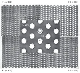
A top view of a 38 × 30 mm organic interposer manufactured.
TL (× 100) TR (× 100)
BR (× 100)
BL (× 100)
(× 500)
(A)
(B)
FIGURE 2.6
25
3D System in Package
the mechanical integrity of the microbumps after the plating process and after aging at 150°C for 72 hours. The results for the bump shear test before
aging are also shown in Reference 3. The average shear force is 3.47 g/bump. After aging, the average shear force decreased to 2.1 g/bump and the growth of intermetallic compound (IMC) Cu6Sn5 is observed [3]. Another approach
for the solder bump pitch reduction and density increase is through a cop-per (Cu) pillar approach. The Cu pillar technology was first introduced to advanced logic devices in 2006 and has since been developed especially for flip chip applications with a bump pitch below 100 μm. Copper pillars are
less prone to electromigration that makes the technology a good choice for applications with reduced bump pitches, sizes, and increased current densi-ties. The Cu pillar interconnection used for 2.5D and 3D IC integration is also referred to as micropillar interconnection. For example, the micropillar array used to connect the current generation of HBM DRAM to interposers has a pitch of 55 μm [15].
2.3 3D SiP for Application-Specific Integrated Circuits and High Bandwidth Memory Integration
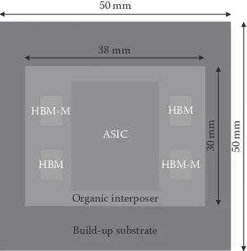
A 3D SiP is designed and manufactured that includes a large-size organic interposer with five Cu wiring layers on each side of the core layer. The organic interposer has a size of 38 × 30 × 0.4 mm. A high-performance ASIC die
mea-sured in 19.1 × 24 × 0.75 mm is attached on top of the organic interposer along
with four HBM DRAM die stacks. The HBM DRAM die stack with a size of 5.5 × 7.7 × 0.48 mm includes one base buffer die and four DRAM-core dice,
which are interconnected with TSVs and fine-pitch micropillars. The HBM stacks are placed equally in quantity along the two sides of the ASIC die. For assessing thermomechanical reliability, two of the HBM stacks are replaced with their daisy-chain versions.
The ASIC and the HBM 3D IC subassembly is then assembled on an organic packaging substrate with the conventional C4 solder bumps. Communications between the ASIC die and the HBM DRAM stacks are made through the Cu wiring and micro-via interconnections of the organic interposer. A top view of the 3D SiP designed is shown schematically
in Figures 2.7 and 2.8 provides a schematic cross-sectional view of the
assembly.
Here HBM-M represents the mechanical or daisy-chain version of the
HBM DRAM stack.
A memory controller and PHY for the HBM were designed and imple-mented for the host ASIC on the organic interposer. To shorten the develop-ment cycle, the ASIC design including the IP for the HBM memory controller and PHY was first implemented through a field-programmable gate arrays (FPGA) device.
2.3.1 Organic Interposer Design
The 38 × 30 mm organic interposer has 12 layers: 5 top routing layers,
2 layers around the core, and 5 bottom routing layers. This configuration is also known as a 5-2-5 layer stack-up. The 50 × 50 mm package substrate has
4 layers: 1 top routing layer, 2 layers around the core, and 1 bottom routing layer. This configuration is known as a 1-2-1 layer stack-up.
Although the package substrate uses regular dielectric material used for standard build-up substrates, the organic interposer is designed and fabricated
HBM
ASIC
HBM
Organic interposer 38 mm
30 mm
HBM-M
HBM-M 50 mm
50 mm
Build-up substrate
FIGURE 2.7
A schematic top view of the 3D SiP designed.
Cu micropillar
HBM ASIC HBM
1-2-1 Build-up substrate
C4 bumps Organic interposer Heat spreader
FIGURE 2.8
27
3D System in Package
with a low-loss dielectric material (0.005@10 GHz loss tangent) and has a coef-ficient of thermal expansion (CTE) closely matched to the CTE of the dielec-tric material used in the packaging substrate. The substrate has an 800 μm
thick core to help minimizing the warpage effects during reflow, whereas the organic interposer has a 200 μm thick core. This new, low-loss dielectric
mate-rial used for the organic interposer allows ultrafine line spacing (line width/ spacing = 6 μm/6 μm), low transmission loss, and high insulation reliability.
2.3.2 Simulation and Results
Time-domain and frequency-domain simulations have been performed to validate the 3D SiP design and to check if the performance specification of the HBM channels is met. The frequency-domain simulations have been done with the Cadence Sigrity PowerSI, whereas for the time-domain simu-lations, HSPICE was used.
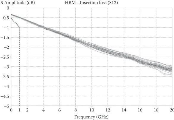
The results for the frequency-domain analysis are shown in Figures 2.9
through 2.11, respectively.
Very good margins, based on standard specifications, for the 0–1 GHz oper-ating frequency bandwidth are achieved. The insertion loss is −0.5 dB@1 GHz
(with −1 dB@1 GHz standard specification), the return loss is approximately −23 dB@1 GHz (with −10 dB@1 GHz standard specification), and the
cross-talk is approximately −45 dB@1 GHz (with −30 dB@1 GHz standard
specifi-cation). The results in these figures also show that in fact good performances are valid for a very high-frequency bandwidth, up to 20 GHz.
0 −5 −4.5 −4 −3.5 −3 −2.5 −2 −1.5 −1 −0.5 0
1 2 4 6 8 10 12
Frequency (GHz)
S Amplitude (dB) HBM - Insertion loss (S12)
14 16 18 20
FIGURE 2.9
0 −80 −70 −60 −50 −40 −30 −20 −15 −10 0
1
0.5 2 4 6 8 10 12
Frequency (GHz)
S Amplitude (dB) HBM - Return loss (S11)
14 16 18 20
FIGURE 2.10
Return loss of the HBM channel simulated.
0 −120 −100 −80 −60 −40 −30 −20 0
1
0.5 2 4 6 8 10 12
Frequency (GHz)
S Amplitude (dB) HBM - X-talk
14 16 18 20
FIGURE 2.11
29
3D System in Package
For the time-domain analysis, multiple corners have been simulated and only the worst-case results are reported here. From the package design file, an HSPICE model was extracted and used for the simulations, along with I/O buffers for the ASIC and HBM memories. The setup used in the HSPICE simulations is shown schematically in Figure 2.12.
A random PRBS 31 (pseudo-random bit sequence) is generated at the input and comparing the resulted sequence at the output with and without any aggressors (one signal was considered victim, and three aggressors on each side) is used to analyze the effect of cross-talk. The results are a comparison for the victim, in the situation with and without the aggressors, so that we can see the output data waveforms when the memory has low activity com-pared to the situation when the memory has high activity. As such, in READ MODE (see block diagram in Figure 2.12), the worst-case skew due to cross-talk is ~46 ps, whereas in WRITE MODE, the worst-case skew is ~42 ps.
Eye diagrams have been computed as well for the two modes. In READ MODE, with cross-talk from aggressors, the eye has a height of ~900 mV
and a width of ~800 ps, and the introduced jitter is about 200 ps. In WRITE
MODE, with cross-talk from aggressors, the eye has a height of ~1 V and a
width of ~825 ps, whereas the introduced jitter is about 175 ps. All the results
mentioned here are with cross-talk and in the worst-case possible. As it can be expected, the results without the cross-talk, in the worst-case, are slightly better. Good confirmation to the frequency-domain results is achieved.
2.4 Three-Dimensional SiP Assembly
To develop the optimal chip joining process for attaching HBM die stacks with micropillars and an overall packaging assembly process flow for the final 3D SiP module, shadow moiré method was used to analyze the
HBM
thermomechanical behavior of each constituent component of the 3D SiP.
Figure 2.13 shows the warpage measurement results for the HBM die stacks
over the temperature range from room temperature to 280°C.
As expected, the warpage of the HBM die stack was small (<8 μm) and did
not change much with temperature.
Figure 2.14 shows the warpage measurement results for the organic
inter-poser from room temperature to 260°C. 0.0
2.0 4.0 6.0 8.0 10.0 12.0 14.0 16.0
25 100 120 150 183 200 220 240 260 280 260 240 220 200 183 150 120 100 25
Wa
rp
age (micron)
Temperature (°C)
HBM_1 HBM_2
FIGURE 2.13
Warpages measured for the HBM die stack from room temperature to 280°C.
0.0 20.0 40.0 60.0 80.0 100.0 120.0 140.0
25 75 90 100 110 120 130 150 183 200 220 240 260 240 220 200 183 150 130 120 110 100 90 75 25
Wa
rp
age (micron)
Temperature (°C)
Interposer_1 Interposer_2
FIGURE 2.14
31
3D System in Package
It can be seen that the warpage of the organic interposer was relatively small (about 100 μm) and stayed in that range when the temperature was
increased up to 260°C.
Based on the thermal deformation analysis for each components of the 3D SiP, a series of design-of-experiments (DOE) were planned and con-ducted to overcome the challenges in developing the suitable assembly process for the ASIC and HBM 3D SiP. As the warpages of the silicon dice and organic interposer were small and did not change with tempera-ture, the ASIC die and HBM DRAM die stacks were assembled onto the interposer to form the ASIC and HBM subassembly first. Underfill encap-sulation was used to protect the joints made of micropillars and regu-lar bumps. A top view and a bottom view of the 3D SiP subassembly are shown in Reference 5.
The structure of the 3D SiP subassembly was then analyzed using X-ray, acoustic, and optical microscopy to ensure good micropillar solder joints are formed. Pictures of the cross-sections for the micropillar joints for attaching HBM die stacks can be found in Reference 5.
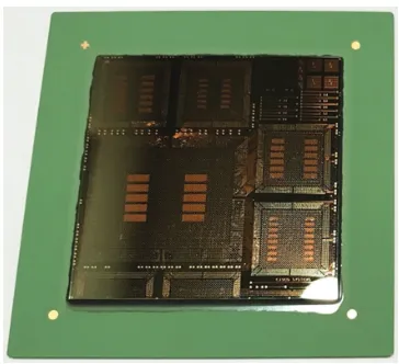
In the final assembly process step, the ASIC and HBM subassembly was attached to the package substrate using the conventional C4 solder bump interconnection. The C4 bumps were then encapsulated using the underfill material. A top view of the finished 3D SiP (without the lid) is shown in
Figure 2.15 and a cross-sectional view of the finished 3D SiP (with the lid) is
shown in Figure 2.16.
FIGURE 2.15
2.5 Test and Characterization
Electrical performance of the ASIC-HBM memory interface and functional-ities of the HBM DRAM stacks as well as post-assembly open and short
per-formance were verified and tested using an application evaluation board designed and fabricated.
The application board with a socket to host the 3D SiP modules was included as part of the test platform. The application board along with a 3D SiP placed in the test socket is shown in Figure 2.17.
The application board measures at 9.5 × 7 inches and has 16 layers: 7
ground layers, 3 power layers and 4 signal layers, and 2 high-speed layers, on the top and bottom of the printed circuit board (PCB). Although the top and bottom layers use Nelco N4000-13 EPSI dielectric material, the other lay-ers use FR4 as dielectric.
Among the communication interfaces present on this application board, an I2C interface was included to provide the communication path from a
Windows PC to the device and to output the results of the tests. The I2C
inter-face was selected due to reuse of the memory controller built-in tests that also included an I2C interface. On the application board, test points and a
connector are also included for testing the daisy-chain connections designed into the organic interposer, JTAG connection for configuring the ASIC, HBM direct access connector, and power distribution and clocking necessary for the operation of the ASIC and the HBM dies. On the PC, a Perl script-driven interface allows for the configuring, running, and analyzing of several
Substrate Interposer HBM
C4 bumps
BGA
HV 10.00 kV
spot 4.0
mag 2 mm
C3SiP module
ASIC (FPGA)
Micro bumps
WD 21.2 mm 100 ×
ASIC
FIGURE 2.16