Physica E 19 (2003) 1 – 5
www.elsevier.com/locate/physe
Silicon nano-transistors for logic applications
Robert Chau
∗, Boyan Boyanov, Brian Doyle, Mark Doczy, Suman Datta,
Scott Hareland, Ben Jin, Jack Kavalieros, Matthew Metz
Components Research, Intel Corporation, 5200 N.E. Elam Young Parkway, Hillsboro, OR 97124, USA
Abstract
Silicon transistors have undergone rapid miniaturization in the past several decades. Recently reported CMOS devices have dimensional scales approaching the “nano-transistor” regime. This paper discusses performance characteristics of a MOSFET device with 15 nm physical gate length. In addition, aspects of a non-planar CMOS technology that bridges the gap between traditional CMOS and the nano-technology era will be presented. It is likely that this non-planar device will form the basic device architecture for future generations of nano-technology.
?2003 Elsevier B.V. All rights reserved.
PACS:85.40.U; 85.30.T
Keywords:Nano-technology—integrated circuits; Transistors—eld eect
1. Introduction
In order to improve performance and density, the size of Si MOS transistor has been scaled aggressively for the past 10 years. Fig.1shows the logic technology node and the corresponding transistor physical gate length (LG) versus year of introduction [1]. It can be
seen that the physical LG has been scaled by more
than 30% every 2 years. The Si MOS transistors that are currently in production have physicalLGof about
70 nm. The physicalLGis expected to decrease and
will reach about 15 nm before 2009, and less than 10 nm early next decade. Research silicon transistors with physicalLGof 20 and 15 nm have already been
demonstrated in our laboratory [2,3]. Considering that an inuenza virus is only 100 nm, the size of silicon transistors produced today in factories and research
∗Corresponding author. Tel.: +1-503-613-6141.
E-mail address:[email protected](R. Chau).
laboratories are already much smaller than a common virus. Thus the size of silicon transistors produced to-day is already in the “nano-regime” and can be termed “silicon nano-transistors”. In this paper, we will show an example of a silicon nano-transistor with 15 nmLG,
discuss the fundamental scaling issues and potential solutions, and talk about a new transistor architec-ture that will become useful later this decade that can easily be considered to be a true bridging technology between conventional CMOS and the beginning of integrated silicon nano-transistors.
2. Silicon nano-transistors and scaling issues
Fig. 2 shows the TEM cross-section of a silicon nano-transistor with 15 nm physicalLG. The height of
the polysilicon gate electrode for this device is 25 nm. The gate oxide used was nitrided SiO2 with physical
thickness of only 0:8 nm [4]. Figs.3 and4show the
0.01 0.10 1.00
1990 1995 2000 2005 2010 Year
Micron
Technology Node
Transistor Physical LG
0.5µm Physical LG
0.5µm Physical LG
0.5µm
Physical L
G0.01 Physical LG
0.5µm Physical LG
0.5µm Physical LG
µ
Physical L
G 30nmFig. 1. Technology node and transistor physicalLG versus year.
Fig. 2. TEM cross-section of a 15 nm MOS transistor.
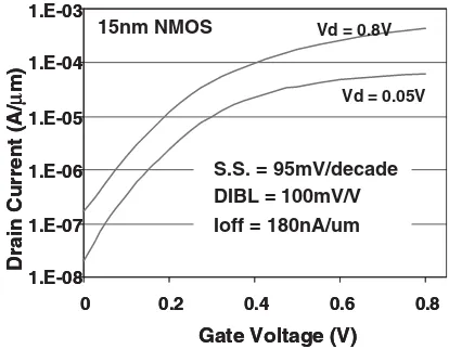
electrical characteristics of this device. It shows very reasonable short channel characteristics with sub-threshold slope of 95 mV=decade and drain-induced barrier lowering (DIBL) of 100 mV=V. At supply voltage of 0:8 V, the transistor has drive current of 0:45 mA=m and o-state leakage of 180 nA=m. Continued improvement in device performance will require further gate oxide scaling, which will require the use of an alternative gate dielectric stack [5], since SiO2 scaling is approaching its limit due to
0.E+00
Drain Voltage (V)
Drain Current (A/µm)
0.8V
0.7V
0.6V
0.5V 15nm CMOS
Fig. 3. FamilyI–V characteristics of the 15 nm MOS transistor.
1.E-08
Gate Voltage (V)
Drain Current (A/
µ
m)
Vd = 0.8V
Vd = 0.05V
S.S. = 95mV/decade DIBL = 100mV/V Ioff = 180nA/um
Gate Voltage (V)
Drain Current (A/
µ
m)
Vd = 0.8V
Vd = 0.05V
S.S. = 95mV/decade DIBL = 100mV/V Ioff = 180nA/um 15nm NMOS
Fig. 4. SubthresholdI–Vcharacteristics of 15 nm MOS transistor.
the increasing gate leakage with oxide scaling and the already-thin physical thickness. Another potential scaling issue is the continual increase in transistor o-state leakage with reducing physicalLG, as shown
1.E-14 1.E-12 1.E-10 1.E-08 1.E-06 1.E-04
10 100 1000
LG (nm)
I
off
(A/µm) 15nm device Production Data Research Data
Fig. 5. Transistor o-state leakage (Io) versus transistor physicalLG.
Fig. 6. Schematic of a Tri-gate transistor.
the requirements of ultra-thin body thickness control needed for control of the electrical characteristics.
3. New transistor architecture for the nano-scale era
A new transistor architecture that can signicantly improve the short-channel performance is the Tri-gate fully depleted silicon substrate transistor, as shown in Fig.6 [7]. This transistor, normally fabricated on an oxide substrate, has a gate electrode on the top and two gate electrodes on the sides of the silicon body. The top-gate transistor has physical gate length
LG and physical gate width WSi, while the side-gate
transistor has physical gate length LG and physical
gate widthTSi, shown in Fig. 6. In general, Tri-gate
transistors will typically have optimal performance
Fig. 7. TEM cross-section of the experimental device.
when LG =WSi =TSi. In contrast to double-gate
non-planar FINFET devices [8] where Wsi ∼ 23LG
or single-gate fully depleted DST [6] devices where
Tsi ∼ 13LG for purposes of controlling short-channel
eects, the Tri-gate transistor has the least strin-gent silicon body thickness and width requirement and is the easiest to fabricate [7]. LG is already
the most stringent lithographic layer in modern CMOS circuits and allowing the Tri-gate to op-erate eectively when LG =WSi =TSi, instead of
sub-LG design features is a tremendous advantage.
A cross-section of an experimental LG = 60 nm
device is shown in Fig. 7 with TSi = 36 nm and WSi = 55 nm. The physical SiO2 thickness is
approximately 1:5 nm measured on the top of the device. The polysilicon gate runs along the vertical sidewalls and the top of the device. Fig.8 shows the
I–V characteristics of the NMOS and PMOS transis-tors in a Tri-gate CMOS with physicalLG= 60 nm.
Both transistors have excellent short channel perfor-mance with DIBL measured at 41 and 48 mV=V for the NMOS and PMOS devices, respectively. Like-wise, the subthreshold slope is excellent with values of 68 mV=decade for the NMOS and 69:5 mV=decade for PMOS. These low values of the subthreshold slope and the absence of a kink demonstrate that the devices are fully depleted. The performance of the NMOS device was measured at IDsat= 1:14 mA=m
VG(Volts)
Vd=-0.05V Vd= 0.05V Vd=1.3V
Vd=-0.05V Vd= 0.05V Vd=1.3V
Vd=-0.05V Vd= 0.05V Vd=1.3V
Vd=-0.05V Vd= 0.05V Vd=1.3V
Fig. 8. Subthreshold I–V characteristics of the 60 nm Tri-gate CMOS.
Fig. 9. Family of curves for the 60 nm Tri-gate CMOS.
The PMOS IDsat was measured at 521A=m at Io= 24 nA=m. In both cases, the normalization per
unit width was measured from the TEM cross-section of the actual experimental device (shown in Fig. 6) and calculated asZ=2TSi+WSi=2×36+55=127 nm. Fig.9illustrates the family of curves for these NMOS and PMOS devices. In order to better understand Tri-gate device performance as the devices are scaled, numerical simulations were performed on a device withLG=WSi=TSi= 30 nm. Fig.10shows the
simu-latedI–V characteristics of a Tri-gate silicon NMOS transistor with physicalLG=Wsi=Tsi= 30 nm done
using a three-dimensional numerical device simula-tor. The 30 nm device has excellent short-channel performance with simulated subthreshold slope of 63 mV=decade (near ideal) and DIBL of 70 mV=V.
0.00 0.10 0.20 0.30 0.40 0.50
VGS (V)
0.00 0.10 0.20 0.30 0.40 0.50
VGS (V)
ID (A)
Fig. 10. SimulatedI–V characteristics of a 30 nm Tri-gate NMOS transistor.
Source
Drain Gate
Multiple Si legs Source
Multiple Si legs
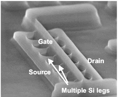
Fig. 11. SEM of the Tri-gate transistor showing multiple Si legs.
In order to increase the total drive current per unit design area, the Tri-gate transistors can be connected in parallel with a common gate electrode as illus-trated in the SEM image reproduced in Fig. 11. The more silicon legs in a given design area, the higher the total drive current will be. Basic scaling shows that the total device current will be current per leg multiplied by the total number of legs. The resulting top-view of the nal layout will look like Fig. 12
S
G
D
S
G
D
multiplelegsS
G
D
S
G
D
S
G
D
S
G
D
multiplelegsFig. 12. Top view of transistor layout comparing the planar (left) and the Tri-gate layout (right) showing multiple Tri-gate legs.
4. Summary
Based on projections, transistor physical LG will
reach about 15 nm before end of this decade. Research silicon nano-transistors with 15 nm physicalLGhave
already been demonstrated with reasonable switching characteristics. Two scaling issues, namely increases in gate and transistor o-state leakage, will need to
be solved in order to control power dissipation in future logic products. The former will require an al-ternative gate stack to solve, and the latter will require a new transistor architecture such as the Tri-gate fully depleted-substrate transistor to solve. In the future, the Tri-gate transistor architecture will be compatible with new electronic devices such as silicon nano-wires, car-bon nano-tubes, or non-Si quantum wire structures.
References
[1] R. Chau, et al., Nikkei Microdevices, February 2002, pp. 83–88.
[2] R. Chau, Silicon Nanoelectronics Workshop, Kyoto, Japan, 2001, pp. 2–3.
[3] B. Doyle, et al., Intel Tech. J. 6 (2) (2002). [4] R. Chau, et al., IEDM (2000) 45 – 48. [5] D. Barlage, et al., IEDM (2001) 231–234. [6] R. Chau, et al., IEDM (2001) 621– 624.