Digital Systems Design with
FPGAs and CPLDs
Ian Grout
AMSTERDAM•BOSTON•HEIDELBERG•LONDON
NEW YORK•OXFORD•PARIS•SAN DIEGO SAN FRANCISCO•SINGAPORE•SYDNEY•TOKYO
Newnes is an imprint of Elsevier
30 Corporate Drive, Suite 400, Burlington, MA 01803, USA Linacre House, Jordan Hill, Oxford OX2 8DP, UK
Copyright2008, Elsevier Ltd. All rights reserved.
Material in Chapter 6 is reprinted, with permission, from IEEE Std 1076–2002 for VHDL Language Reference Manual, by IEEE. The IEEE disclaims any responsibility or liability resulting from placement and use in the manner described.
MATLABand Simulinkare trademarks of The MathWorks, Inc. and are used with permission. The MathWorks does not
warrant the accuracy of the text or exercises in this book. This book’s use or discussion of MATLABand Simulink
software or related products does not constitute endorsement or sponsorship by The MathWorks of a particular pedagogical approach or particular use of the MATLABand Simulinksoftware.
Figures based on or adapted from figures and text owned by Xilinx, Inc., courtesy of Xilinx, Inc. CopyrightXilinx, Inc., 1995–2005. All rights reserved.
Microsoft product screen shot(s) reprinted with permission from Microsoft Corporation.
No part of this publication may be reproduced, stored in a retrieval system, or transmitted in any form or by any means, electronic, mechanical, photocopying, recording, or otherwise, without the prior written permission of the publisher.
Permissions may be sought directly from Elsevier’s Science & Technology Rights Department in Oxford, UK:
phone: (þ44) 1865 843830, fax: (þ44) 1865 853333, E-mail: [email protected]. You may also complete your request online via the Elsevier homepage (http://elsevier.com), by selecting ‘‘Support & Contact’’ then ‘‘Copyright and Permission’’ and then ‘‘Obtaining Permissions.’’
Recognizing the importance of preserving what has been written, Elsevier prints its books on acid-free paper whenever possible.
Library of Congress Cataloging-in-Publication Data
Grout, Ian.
Digital systems design with FPGAs and CPLDs / Ian Grout. p. cm.
Includes bibliographical references and index.
ISBN-13: 978-0-7506-8397-5 (alk. paper) 1. Digital electronics. 2. Digital circuits — Design and construction. 3. Field programmable gate arrays. 4. Programmable logic devices. I. Title.
TK7868.D5.G76 2008 621.381—dc22
2007044907
British Library Cataloguing-in-Publication Data
A catalogue record for this book is available from the British Library.
For information on all Newnes publications visit our Web site at www.books.elsevier.com
Printed in the United States of America
08 09 10 11 12 13 10 9 8 7 6 5 4 3 2 1
Table of Contents
Preface ...xvii
Abbreviations ...xxiii
Chapter 1: Introduction to Programmable Logic ... 1
1.1 Introduction to the Book ...1
1.2 Electronic Circuits: Analogue and Digital ...10
1.2.1 Introduction ...10
1.2.2 Continuous Time versus Discrete Time...10
1.2.3 Analogue versus Digital ...12
1.3 History of Digital Logic ...14
1.4 Programmable Logic versus Discrete Logic ...17
1.5 Programmable Logic versus Processors ...21
1.6 Types of Programmable Logic ...24
1.6.1 Simple Programmable Logic Device (SPLD) ...24
1.6.2 Complex Programmable Logic Device (CPLD) ...27
1.6.3 Field Programmable Gate Array (FPGA)...28
1.7 PLD Configuration Technologies ...29
1.8 Programmable Logic Vendors...32
1.9 Programmable Logic Design Methods and Tools...33
1.9.1 Introduction ...33
1.9.2 Typical PLD Design Flow...35
1.10 Technology Trends ...36
References ...38
Student Exercises ...40
Chapter 2: Electronic Systems Design ... 43
2.1 Introduction ...43
2.2.1 Introduction ...52
2.2.2 Sequential Product Development Process ...53
2.2.3 Concurrent Engineering Process...54
2.3 Flowcharts...56
2.4 Block Diagrams...58
2.5 Gajski-Kuhn Chart ...61
2.6 Hardware-Software Co-Design ...62
2.7 Formal Verification...65
2.8 Embedded Systems and Real-Time Operating Systems ...66
2.9 Electronic System-Level Design ...67
2.10 Creating a Design Specification...68
2.11 Unified Modeling Language...70
2.12 Reading a Component Data Sheet ...72
2.13 Digital Input/Output ...75
2.13.1 Introduction...75
2.13.2 Logic-Level Definitions ...79
2.13.3 Noise Margin...81
2.13.4 Interfacing Logic Families ...83
2.14 Parallel and Serial Interfacing ...89
2.14.1 Introduction...89
2.14.2 Parallel I/O ...95
2.14.3 Serial I/O ...97
2.15 System Reset... 102
2.16 System Clock ... 105
2.17 Power Supplies ... 107
2.18 Power Management... 109
2.19 Printed Circuit Boards and Multichip Modules ... 110
2.20 System on a Chip and System in a Package... 112
2.21 Mechatronic Systems... 113
2.22 Intellectual Property ... 115
2.23 CE and FCC Markings ... 116
References... 118
Student Exercises ... 121
Chapter 3: PCB Design ... 123
3.1 Introduction ... 123
3.2 What Is a PCB? ... 125
3.2.1 Definition ... 125
3.2.2 Structure of the PCB ... 127
3.2.3 Typical Components... 139
3.3 Design, Manufacture, and Testing ... 144
3.3.1 PCB Design ... 144 viii Table of Contents
3.3.2 PCB Manufacture... 150
3.3.3 PCB Testing... 151
3.4 Environmental Issues ... 152
3.4.1 Introduction ... 152
3.4.2 WEEE Directive ... 153
3.4.3 RoHS Directive ... 153
3.4.4 Lead-Free Solder ... 154
3.4.5 Electromagnetic Compatibility ... 154
3.5 Case Study PCB Designs... 155
3.5.1 Introduction ... 155
3.5.2 System Overview ... 157
3.5.3 CPLD Development Board ... 158
3.5.4 LCD and Hex Keypad Board ... 160
3.5.5 PC Interface Board... 163
3.5.6 Digital I/O Board ... 166
3.5.7 Analogue I/O Board... 168
3.6 Technology Trends... 171
References ... 173
Student Exercises ... 175
Chapter 4: Design Languages... 177
4.1 Introduction ... 177
4.2 Software Programming Languages ... 177
4.2.1 Introduction ... 177
4.2.2 C ... 179
4.2.3 Cþþ... 181
4.2.4 JAVATM... 183
4.2.5 Visual BasicTM... 186
4.2.6 Scripting Languages ... 189
4.2.7 PHP ... 191
4.3 Hardware Description Languages ... 193
4.3.1 Introduction ... 193
4.3.2 VHDL ... 194
4.3.3 Verilog-HDL ... 196
4.3.4 Verilog-A... 199
4.3.5 VHDL-AMS... 202
4.3.6 Verilog-AMS ... 205
4.4 SPICE... 205
4.5 SystemC... 208
4.6 SystemVerilog... 209
4.7 Mathematical Modeling Tools ... 210
References ... 214
Chapter 5: Introduction to Digital Logic Design ... 217
5.1 Introduction ... 217
5.2 Number Systems... 222
5.2.1 Introduction ... 222
5.2.2 Decimal–Unsigned Binary Conversion... 224
5.2.3 Signed Binary Numbers... 226
5.2.4 Gray Code ... 231
5.2.5 Binary Coded Decimal ... 232
5.2.6 Octal-Binary Conversion ... 233
5.2.7 Hexadecimal-Binary Conversion ... 235
5.3 Binary Data Manipulation ... 240
5.3.1 Introduction ... 240
5.3.2 Logical Operations ... 241
5.3.3 Boolean Algebra ... 242
5.3.4 Combinational Logic Gates ... 246
5.3.5 Truth Tables ... 248
5.4 Combinational Logic Design ... 256
5.4.1 Introduction ... 256
5.4.2 NAND and NOR logic ... 269
5.4.3 Karnaugh Maps ... 271
5.4.4 Don’t CareConditions... 277
5.5 Sequential Logic Design... 277
5.5.1 Introduction ... 277
5.5.2 Level Sensitive Latches and Edge-Triggered Flip-Flops ... 282
5.5.3 The D Latch and D-Type Flip-Flop ... 283
5.5.4 Counter Design... 288
5.5.5 State Machine Design... 305
5.5.6 Moore versus Mealy State Machines ... 316
5.5.7 Shift Registers... 317
5.5.8 Digital Scan Path... 319
5.6 Memory... 322
5.6.1 Introduction ... 322
5.6.2 Random Access Memory ... 324
5.6.3 Read-Only Memory... 325
References... 327
Student Exercises ... 328
Chapter 6: Introduction to Digital Logic Design with VHDL ... 333
6.1 Introduction ... 333
6.2 Designing with HDLs ... 334 x Table of Contents
6.3 Design Entry Methods ... 338
6.3.1 Introduction ... 338
6.3.2 Schematic Capture... 338
6.3.3 HDL Design Entry ... 339
6.4 Logic Synthesis... 341
6.5 Entities, Architectures, Packages, and Configurations... 344
6.5.1 Introduction ... 344
6.5.2 AND Gate Example ... 346
6.5.3 Commenting the Code... 353
6.6 A First Design ... 355
6.6.1 Introduction ... 355
6.6.2 Dataflow Description Example ... 356
6.6.3 Behavioral Description Example ... 357
6.6.4 Structural Description Example ... 359
6.7 Signals versus Variables ... 366
6.7.1 Introduction ... 366
6.7.2 Example: Architecture with Internal Signals ... 368
6.7.3 Example: Architecture with Internal Variables ... 372
6.8 Generics... 374
6.9 Reserved Words ... 380
6.10 Data Types ... 380
6.11 Concurrent versus Sequential Statements... 383
6.12 Loops and Program Control ... 383
6.13 Coding Styles for VHDL... 385
6.14 Combinational Logic Design... 387
6.14.1 Introduction... 387
6.14.2 Complex Logic Gates ... 388
6.14.3 One-Bit Half-Adder ... 388
6.14.4 Four-to-One Multiplexer ... 389
6.14.5 Thermometer-to-Binary Encoder... 397
6.14.6 Seven-Segment Display Driver ... 398
6.14.7 Tristate Buffer ... 409
6.15 Sequential Logic Design ... 414
6.15.1 Introduction... 414
6.15.2 Latches and Flip-Flops... 416
6.15.3 Counter Design... 422
6.15.4 State Machine Design... 426
6.16 Memories... 440
6.16.1 Introduction... 440
6.16.2 Random Access Memory... 441
6.16.3 Read-Only Memory... 444
6.17 Unsigned versus Signed Arithmetic ... 447
6.17.2 Adder Example... 448
6.17.3 Multiplier Example... 449
6.18 Testing the Design: The VHDL Test Bench... 453
6.19 File I/O for Test Bench Development ... 459
References... 471
Student Exercises... 472
Chapter 7: Introduction to Digital Signal Processing ... 475
7.1 Introduction ... 475
7.2 Z-Transform... 496
7.3 Digital Control ... 509
7.4 Digital Filtering... 524
7.4.1 Introduction ... 524
7.4.2 Infinite Impulse Response Filters ... 532
7.4.3 Finite Impulse Response Filters ... 534
References... 535
Student Exercises... 536
Chapter 8: Interfacing Digital Logic to the Real World: A/D Conversion, D/A Conversion, and Power Electronics ... 537
8.1 Introduction ... 537
8.2 Digital-to-Analogue Conversion ... 543
8.2.1 Introduction ... 543
8.2.2 DAC Characteristics... 548
8.2.3 Types of DAC ... 555
8.2.4 DAC Control Example... 559
8.3 Analogue-to-Digital Conversion ... 565
8.3.1 Introduction ... 565
8.3.2 ADC Characteristics... 568
8.3.3 Types of ADC ... 572
8.3.4 Aliasing... 577
8.4 Power Electronics ... 580
8.4.1 Introduction ... 580
8.4.2 Diodes ... 581
8.4.3 Power Transistors... 585
8.4.4 Thyristors ... 593
8.4.5 Gate Turn-Off Thyristors ... 603
8.4.6 Asymmetric Thyristors ... 604
8.4.7 Triacs ... 604
8.5 Heat Dissipation and Heatsinks... 606
8.6 Operational Amplifier Circuits... 610 xii Table of Contents
References... 612
Student Exercises... 613
Chapter 9: Testing the Electronic System ... 615
9.1 Introduction ... 615
9.2 Integrated Circuit Testing ... 621
9.2.1 Introduction ... 621
9.2.2 Digital IC Testing... 624
9.2.3 Analogue IC Testing ... 629
9.2.4 Mixed-Signal IC Testing... 633
9.3 Printed Circuit Board Testing ... 633
9.4 Boundary Scan Testing ... 636
9.5 Software Testing... 642
References... 645
Student Exercises... 646
Chapter 10: System-Level Design ... 647
10.1 Introduction ... 647
10.2 Electronic System-Level Design ... 654
10.3 Case Study 1: DC Motor Control ... 661
10.3.1 Introduction... 661
10.3.2 Motor Control System Overview... 662
10.3.3 MATLAB/SimulinkModel Creation and Simulation ... 665
10.3.4 Translating the Design to VHDL ... 666
10.3.5 Concluding Remarks ... 674
10.4 Case Study 2: Digital Filter Design... 686
10.4.1 Introduction... 686
10.4.2 Filter Overview ... 688
10.4.3 MATLAB/SimulinkModel Creation and Simulation ... 690
10.4.4 Translating the Design to VHDL ... 692
10.4.5 Concluding Remarks ... 698
10.5 Automating the Translation ... 702
10.6 Future Directions ... 703
References... 704
Student Exercises ... 705
Additional References ... 707
•noun 1A set of things working together as parts of a mechanism or an interconnecting network.
Preface
In days gone by, life for the electronic circuit designer seems to have been easier. Designs were smaller, ran at a slower speed, and could easily fit onto a single small printed circuit board. An individual designer could work on a problem and designs could be specified and developed using paper and pen only. The circuit schematic diagrams that were required could be rapidly drawn on the back of an envelope.
Struck by the success of the early circuit designs, customers started to ask for smaller, faster, and more complex circuits—and at a lower cost. The designers started to work on solving such problems, which has led to the rapidly expanding electronics industry that we have today. Driven by the demand from the customer, new materials and fabrication processes have been developed, new circuit design methodologies and design architectures have taken over many of the early traditional design approaches, and new markets for the circuits have evolved.
effective system-level specification to an efficient and working circuit implementation requires the skills of good designers who are aided by good design tools.
For the electronic circuit designer at an early stage in the design process, whether to implement the required circuit functionality using analogue circuit techniques or digital circuit techniques must be decided. However, sometimes the choice will have already been made, and increasingly a digital solution is the preferred choice. The wide use of digital signal processing (DSP) techniques facilitates complex operations that can provide superior performance to an analogue circuit equivalent; indeed some cannot be performed in analogue. Traditionally, DSP functions have been implemented using software programs written to operate on a target processor. The microprocessor (mP), microcontroller (mC), and digital signal processor provide the necessary digital circuits, in integrated circuit (IC) form, to implement the required functions. In fact, these processors are to be found in many everyday embedded electronics that we take for granted. This book could not have been written without the aid of an electronic system incorporating a microprocessor running a software operating system that in turn runs the word processor software.
Increasingly, the functions that have been traditionally implemented in software running on a processor-based digital system in the DSP world and many control applications are being evaluated in terms of performance that can be achieved in software. In many cases, the software solution will be slower than is desired, and the basic nature of the software programmed system means that this speed limitation cannot be overcome. The way to overcome the speed limitation is to perform the required operations in hardware designed for a particular application. However, custom hardware solutions will be expensive to acquire.
If there were a way to obtain the power of programmability with the power of hardware speed, then this would be provide a significant way forward.
Fortunately, programmable logic provides the power of programmability with the power of hardware speed by providing an IC with built-in digital electronic circuitry that is configured by the user for a particular application. Many devices can be reconfigured for different applications. Today, two main types of programmable logic ICs are commonly used: the field programmable gate array (FPGA) and complex programmable logic device (CPLD).
Therefore, it is possible to implement a complex digital system that can be developed and the functionality changed or enhanced using either a processor running a software program or programmable logic with a specific hardware configuration.
xviii Preface
For an end-user, the functionality of both types of system will be the same—the design details are irrelevant to the end-user as long as the functionality of the unit is correct. In this book, to provide consistency and to differentiate between the processor and programmable logic, the following terminology will be used:
• Aprocessor(microprocessor, mP; microcontroller,mC; or digital signal processor, DSP) will beprogrammedfor a particular application using a software programming language(SPL).
• Programmable logic(field programmable gate array, FPGA; simple
programmable logic device, SPLD; or complex programmable logic device, CPLD) will beconfiguredusing ahardware description language(HDL). The aim of this book is to provide a reference source with worked examples in the area of electronic circuit design using programmable logic. In particular, field programmable gate arrays and complex programmable logic devices will be presented and examples of such devices provided.
The choice whether to use a software-programmed processor or hardware-configured programmable logic device is not a simple one, and many decisions figure into evaluating the pros and cons of a particular implementation prior to making a final decision. This book will provide an insight into the design capabilities and aspects relating to the design decisions for programmable logic so that an informed decision can be made.
The book is structured as follows:
Chapter 1 will introduce the types of programmable logic device that are available today, their differing architectures, and their use within electronic system design. Additionally, the terminology used in this area will be presented with the aim of demystifying the jargon that has evolved.
ensure that the different electronic circuit components interact with each other correctly and do not provide unwanted effects. A correctly designed PCB will allow the circuit to perform as intended. A badly designed PCB will prevent the circuit from working altogether.
Chapter 4will discuss the different programming languages that are used to develop digital designs for implementation in either a processor (software-programmed microprocessor, microcontroller, or digital signal processor) or in programmable logic (hardware-configured FPGA or CPLD). The main languages used will be introduced and examples provided. For programmable logic, the main hardware description languages used are Verilog-HDL and VHDL (VHSIC Hardware Description Language). These are IEEE (Institute of Electrical and Electronics Engineers) standards, universally used in both education and industry.
Chapter 5will introduce digital logic design principles. A basic understanding of the principles of digital circuit design, such as Boolean Logic, Karnaugh maps, and counter/state machine design will be expected. However, a review of these principles will be provided for designs in schematic diagram form and presented such that the design functionality may be mapped over a VHDL description in Chapter 6.
Chapter 6 will introduce VHDL as one of the IEEE standard hardware description languages available to describe digital circuit and system designs in an ASCII text-based format. This description can be simulated and synthesized. (Simulation will validate the design operation, and synthesis will translate the text-based description into a circuit design in terms of logic gates and the interconnections between the basic logic gates. The gates and gate connections are commonly referred to as the netlist.) The design examples provided in schematic diagram form in Chapter 5 will be revisited and modeled in VHDL.
Chapter 7 will introduce the development of digital signal processing algorithms in VHDL and the synthesis of the VHDL descriptions to target programmable logic (both FPGA and CPLD). Such algorithms include digital filters (low-pass, high-pass, and band-pass), digital PID (proportional plus integral plus derivative) control algorithms, and the FFT (fast Fourier transform, an efficient implementation of the discrete Fourier transform, DFT).
Chapter 8 will discuss the interfacing of programmable logic to what is commonly referred to as the real world. This is the analogue world that we live in, and such interfacing requires both the acquisition (capture) and the generation of analogue
xx Preface
signals. To enable this, the digital programmable logic device will require an interface to the analogue world. For analogue signals to be captured and analyzed in digital, an analogue-to-digital converter (ADC) will be required. For analogue signals to be generated from the digital, a digital-to-analogue converter (DAC) will be required.
In this book, the convention used for the wordanaloguewill use the -ue at the end of the word, unless a particular name already in use is referred to spelled asanalog. Chapter 9will introduce the testing of the electronic system. In this, failure mechanisms in hardware and software will be introduced, and the need for efficient and
cost-effective test programs from the prototyping phase of the design through high-volume manufacture and in-system testing.
Chapter 10 will introduce the increasing need to develop programmable logic–based designs at a high level of abstraction using behavioral descriptions of the system functionality, and the increasing requirements to enable the synthesis of these high-level designs into logic. With reference to a design flow taking a digital design developed in MATLABor Simulinkthrough a VHDL code equivalent for implementation in FPGA or CPLD technology, the synthesis of digital control system algorithms modeled and simulated in Simulinkwill be translated into VHDL for implementation in programmable logic.
Throughout the book, the HDL examples provided and evaluated can be implemented within programmable logic–based circuits that may be designed by the user in addition to the PCB design examples that are provided. These examples have been developed to form the basis of laboratory experiments that can be used to accompany the text. With the broad range of subject material and examples, a feature of the book is its potential for use in a range of learning and teaching scenarios. For example:
1. As an introduction to design of electronic circuits and systems using programmable logic. This would allow for the design approaches, programmable logic architectures, simulation, synthesis, and the final configuration of an FPGA or CPLD to be undertaken. It would also allow for investigation into the most appropriate HDL coding styles and device implementation constraints to be undertaken.
code working on real devices and to enable additional testing of the electronic circuit with such equipment as oscilloscopes and spectrum analyzers.
3. As an introduction to the design of printed circuit boards, in particular mixed-signal designs (mixed analogue and digital). This would allow issues relating to the design of the printed circuit board to be investigated and designs developed, fabricated, and tested.
4. As an introduction to digital signal processing algorithm development. This would allow the basics of DSP algorithms and their implementation in hardware on FPGAs and CPLDs to be investigated through the medium of VHDL code development, simulation, and synthesis.
The VHDL examples can be downloaded and run on the hardware prototyping arrangement that can be built by the reader using the designs provided in the book. This hardware arrangement is centered on a XilinxCoolrunnerTM-II CPLD on which to prototype the digital logic ideas, along with a set of input/output (I/O) boards. The full set of boards is shown in the figure below.
This arrangement consists of five main system boards and an optional seven-segment display board. The appendices and design schematics are available at the author’s Web site for this book (refer to http://books.elsevier.com/companions/ 9780750683975 and follow the hyperlink to the author’s site).
Abbreviations
A
AC alternating current
ADC analogue-to-digital converter
ALU arithmetic and logic unit
AM amplitude modulation
AMD advanced micro devices
AMS analogue and mixed-signal
AND logical AND operation on two or more digital signals
ANSI American National Standards Institute
AOI automatic optical inspection
ASCII American Standard Code for Information Interchange
ASIC application-specific integrated circuit
ASP analogue signal processor
ASSP application-specific standard product
ATA AT attachment
ATE AT equipment
ATPG AT program generation
AWG arbitrary waveform generator
American wire gauge
AXI automatic X-ray inspection
B
BASIC Beginner’s All-purpose Symbolic Instruction Code
BCD binary coded decimal
BGA ball grid array
BiCMOS bipolar and CMOS
bit binary digit
BJT bipolar junction transistor
BNC bayonet Neill-Concelman connector
BPF band-pass filter
BSDL boundary scan description language
BS(I) British Standards (Institution)
BST boundary scan test
C
CAD computer-aided design
CAE computer-aided engineering
CAM computer-aided manufacture
CAT computer-aided test
CBGA ceramic BGA
CD compact disk
CE chip enable
CERDIP ceramic DIP
CERQUAD ceramic quadruple side
CIC cascaded integrator comb
CISC complex instruction set computer
CLB configurable logic block
CLCC ceramic leadless chip carrier
ceramic leaded chip carrier
CMOS complementary metal oxide semiconductor
COTS commercial off-the-shelf
CPGA ceramic PGA
CPLD complex PLD
CPU central processing unit
CQFP ceramic quad flat pack
CS chip select
CSOIC ceramic SOIC
CSP chip scale packaging
CSSP customer specific standard product
CTFT continuous-time Fourier transform
CTS clear to send
CUT circuit under test
xxiv Abbreviations
D
DAC digital-to-analogue converter
DAE differential and algebraic equation
DAQ data acquisition
dB decibel
DBM digital boundary module
DC direct current
DCD data carrier detected
DCE data communication equipment
DCI digitally controlled impedance
DCPSS DC power supply sensitivity
DDC direct digital control
DDR double data rate
DDS direct digital synthesis
DfA design for assembly
DfD design for debug
DFF D-type flip-flop
DfM design for manufacturability
DfR design for reliability
DfT design for testability
DFT discrete Fourier transform
DfX design for X
DfY design for yield
DIB device interface board
DIL dual in-line
DIMM dual in-line memory module
DIP dual in-line package
DL defect level
DMM digital multimeter
DNL differential nonlinearity
DoD U.S. Department of Defense
DPLL digital PLL
dpm defects per million
DR data register
DRAM dynamic RAM
DRDRAM direct Rambus DRAM
DSM deep submicron
DSP digital signal processing
digital signal processor
DSR data set ready
DTE data terminal equipment
DTFT discrete-time Fourier transform
DTR data terminal ready
DUT device under test
DVD digital versatile disk
E
EC European Commission
ECL emitter coupled logic
ECU electronic control unit
EDA electronic design automation
EDIF electronic design interchange format
EHF extremely high frequency
EIAJ Electronic Industries Association of Japan
ELF extremely low frequency
EMC electromagnetic compatibility
EMI electromagnetic interference
ENB effective number of bits
EOC end of conversion
EOS electrical overstress
EEPROM electrically erasable PROM
E2EPROM electrically erasable PROM
EPROM erasable PROM
ERC electrical rules checking
ESD electrostatic discharge
ESIA European Semiconductor Industry Association
ESL electronic system level
ESS environmental stress screening
EU European Union
EX-NOR NOT-EXCLUSIVE-OR
EX-OR logical EXCLUSIVE-OR operation on two or more digital
signals xxvi Abbreviations
F
F Farad
FA failure analysis
FBGA (FPBGA) fine pitch ball grid array
FCC Federal Communications Commission (USA)
FET field effect transistor
FFT fast Fourier transform
FIFO first-in, first-out
FIR finite impulse response
FM frequency modulation
FPAA field programmable analogue array
FPGA field programmable gate array
FPT flying probe tester
FR-4 flame retardant with approximate dielectric constant of 4
FRAM ferromagnetic RAM
FSM finite state machine
FT functional tester
G
GaAs gallium arsenide
GAL generic array of logic
GDSII Graphic Data System II stream file format
GND ground
GPIB general purpose interface bus
GTL Gunning transceiver logic
GTO gate turn-off thyristor
GUI graphical user interface
H
HBM human body model
HBT heterojunction bipolar transistor
HDIP hermetic DIP
HDL hardware description language
HF high frequency
HPF high-pass filter
HSTL high-speed transceiver logic
HVI human visual inspection
HW hardware
Hz Hertz
I
IB base current
IBM base peak current
IC collector current
ICC power supply current (into VCCpin for bipolar circuits)
ICM collector peak current
IDD power supply current (into VDDpin for CMOS circuits)
IDDQ quiescent power supply current (IDD)
IEE power supply current (out of VEEpin for bipolar circuits)
IFS full-scale current
IGND ground current per supply pin
IIH high-level input current
IIL low-level input current
ILSB minimum output current change
IO output current
IOH high-level output current (logic 1 output)
IOL low-level output current (logic 0 output)
IOS offset current
IOUT output current
IREF reference current
ISS power supply current (out of VSSpin for CMOS circuits)
ISSQ quiescent power supply current (ISS)
IC integrated circuit
I2C (IIC) inter-integrated circuit (inter-IC) bus
I2S inter-IC sound bus
ICT in-circuit test
in-circuit tester
IDC insulation displacement connector
IDE integrated design environment
integrated drive electronics
IEC International Electrotechnical Commission
IEE Institution of Electrical Engineers
IEEE Institute of Electrical and Electronics Engineers xxviii Abbreviations
IET Institution of Engineering and Technology
IIR infinite impulse response
IMAPS International Microelectronics and Packaging Society
INL integral nonlinearity
I/O input/output
IP intellectual property
IR instruction register
infrared
ISO International Organization for Standardization
ISP in-system programmable
ISR in-system reprogrammable
IT information technology
ITRS International Technology Roadmap for Semiconductors
I-V current-to-voltage
J
JDK JAVATMDevelopment Kit
JEDEC Joint Electron Device Engineering Council
JEITA Japan Electronics and Information Technology Industries
Association
JETAG Joint European Test Action Group
JETTA Journal of Electronic Testing, Theory, and Applications
JFET junction FET
JLCC J-leaded chip carrier
JTAG Joint Test Action Group
K
KGD known good die
KSIA Korean Semiconductor Industry Association
L
LAN local area network
LC logic cell
LC2MOS linear compatible CMOS
LCC leaded chip carrier
leadless chip carrier
LCCMOS leadless chip carrier metal oxide semiconductor (also LC2MOS)
LCD liquid crystal display
LF low frequency
LFSR linear feedback shift register
LIFO last-in, first-out
Linux Linux is not Unix
LPF low-pass filter
LSB least significant bit
LSI large-scale integration
LUT look-up table
LVCMOS low-voltage CMOS
LVDS low-voltage differential signaling
LVS layout versus schematic
LVTTL low-voltage TTL
M
mBGA micro ball grid array
mC microcontroller
mP microprocessor
MATLAB Matrix Laboratory (from The Mathworks, Inc.)
MAX maximum
MCM multichip module
MCU microcontroller unit
MEMs micro electro-mechanical systems
MF medium frequency
MIL military
MIN minimum
MISR multiple-input signature register
MM machine model
MOS metal oxide semiconductor
MOSFET metal oxide semiconductor field effect transistor
MPGA mask programmable gate array
MS Microsoft
MSAF multiple stuck-at-fault
MSB most significant bit
MSI medium-scale integration
MSOP mini-small outline package
MUX multiplexer
MVI manual visual inspection (i.e., HVI)
xxx Abbreviations
N
NAND NOT-AND
NDI normal data input
NDO normal data output
NDT nondestructive test
NMH noise margin for high levels
NML noise margin for low levels
nMOS n-channel MOS
NOR NOT-OR
NOT logical NOT operation on a single digital signal
NRE nonrecurring engineering
NVM nonvolatile memory
NVRAM nonvolatile RAM
O
OE output enable
OEM original equipment manufacturer
ONO oxide-nitride-oxide
OOP object-oriented programming
op-amp operational amplifier
OR logical OR operation on two or more digital signals
OS operating system
OSR oversampling ratio
OTP one-time programmable
OVI Open Verilog International
P
Ptot total dissipation
PAL programmable array of logic
PBGA plastic BGA
PC personal computer
program counter
PCB printed circuit board
PCBA printed circuit board assembly
PCI PC interface
PDF portable document format
PDIL plastic DIL
PDIP plastic DIP
PERL practical extraction and report language
PGA pin grid array
PI primary input
proportional plus integral
PID proportional plus integral plus derivative
PIPO parallel in, parallel out
PLA programmable logic array
PLCC plastic leadless chip carrier
plastic leaded chip carrier
PLD programmable logic device
PLL phase-locked loop
PM phase modulation
pMOS p-channel MOS
PMU precision measurement unit
PO primary output
PoC proof of concept
PoP package on package
POR power-on reset
PPGA plastic PGA
ppm parts per million
PQFP plastic QFP
PROM programmable ROM
PRPG pseudorandom pattern generator
PSOP plastic SOP
PWB printed wiring board
PWM pulse width modulation
pulse width modulated
PXI PC extensions for instrument bus
Q
QFJ quad flat pack (J-lead)
QFP quad flat pack
QSOP quarter-size SOP
QTAG Quality Test Action Group
xxxii Abbreviations
R
trademark (registered;TM for unregistered)
RAM random access memory
RC resistor-capacitor
RD read
received data
RF radio frequency
RI ring indicator
RISC reduced instruction set computer
RMS root mean squared
RoHS return of hazardous substances
ROM read-only memory
RTL register transfer level
RTOS real-time operating system
RTS ready to send
RWM read-write memory (also referred to as RAM)
Rx receiver
S
D sigma-delta
SA0 stuck-at-0
SA1 stuck-at-1
SAF stuck-at-fault
SAR successive approximation register
SCR silicon-controlled rectifier
SCSI small computer system interface
SDRAM synchronous DRAM
SDI scan data input
SDO scan data out
SE scan enable
SFDR spurious free dynamic range
SG signal ground
SHF super high frequency
SI signal integrity
SiGe silicon germanium
SIM subscriber identity module
SINAD signal to noise plus distortion (SNRþTHD)
SiP system in a package
SIP single in-line package
SIPO serial in, parallel out
SISO Serial in, serial out
Single input, single output
SISR serial input signature register
SLDRAM synchronous-link DRAM
SMT surface mount technology
SNR signal-to-noise ratio
S/(NþTHD) signal to noise plus total harmonic distortion
SOAR safe operating region
SoB system on board
SoC system on a chip
SOC start of conversion
SOI silicon on insulator
SOIC small outline IC
SOJ small outline J-lead package
SOP small outline package
SPGA staggered PGA
SPI serial peripheral interface
SPICE simulation program with integrated circuit emphasis
SPL software programming language
SPLD simple PLD
SQFP shrink quad flat pack
SRAM static RAM
SRBP synthetic resin-bonded paper
SSAF single stuck-at-fault
SSI small-scale integration
SSOP small shrink outline package
SSTL stub series terminated logic
STC Semiconductor Test Consortium
STD standard
STIL standard test interface language
SW software
xxxiv Abbreviations
T
TL lead temperature
Tstg storage temperature
TAB tape automated bonding
TAP test access port
TCE thermal coefficient of expansion
TCK test clock
Tcl tool command language
TD transmitted data
TDI test data input
TDO test data output
THD total harmonic distortion
TM trademark (unregistered,
for registered)
TMS test mode select
TO transistor outline package (single transistor)
TPG test program generation
TQFP thin QFP
TRST test reset
TSIA Taiwan Semiconductor Industry Association
TSMC Taiwan Semiconductor Manufacturing Company
TSOP thin SOP
TSSOP thin shrink SOP
TVSOP thin very SOP
TTL transistor-transistor logic
TTM time to market
TYP typical
Tx transmitter
U
UART universal asynchronous receiver/transmitter
UHF ultra high frequency
UJT unijunction transistor
ULSI ultra large-scale integration
UML unified modeling language
UNIXTM Uniplexed Information and Computing System (originally
Unics, later renamed Unix)
UTP unit test period
UUT unit under test
UV ultraviolet
V
VCB collector-base voltage
VCC power supply voltage (positive, for bipolar circuits)
VCE0 collector-emitter voltage (IE =0)
VCEV collector-emitter voltage (VBE= 1.5)
VDD power supply voltage (positive, for CMOS circuits)
VEB emitter-base voltage
VEE power supply voltage (negative, for bipolar circuits)
VFS full-scale voltage
VFSR full-scale range of voltage
VI input voltage
VIH minimum input voltage that can be interpreted as a logic 1
VIL maximum input voltage that can be interpreted as a logic 0
VLSB minimum output voltage change
VO output voltage
VOH minimum output voltage when the output is a logic 1
VOL maximum output voltage when the output is a logic 0
VOS offset voltage
VOUT output voltage
VREF reference voltage
VSS power supply voltage (negative, for CMOS circuits)
VASG VHDL Analysis and Standardization Group
VB Visual BasicTM
VBA Visual BasicTMfor Applications
VCO voltage-controlled oscillator
VDSM very deep submicron
VDU visual display unit
VF voice frequency
VHDL VHSIC hardware description language
VHF very high frequency
VHSIC very high-speed integrated circuit
VLF very low frequency
xxxvi Abbreviations
VLSI very large-scale integration
VQFP very thin quad flat pack
W
WE write enable
WEEE waste electrical and electronic equipment
WR write
WSI wafer-scale integration
X
XNF Xilinx Netlist format
Z
ZIF zero insertion force socket
Introduction to Programmable Logic
1.1
Introduction to the Book
Increasingly, electronic circuits and systems are being designed using technologies that offer rapid prototyping, programmability, and re-use (reprogrammability and component recycling) capabilities to allow a system product to be developed in a minimal time, to allow in-service reconfiguration (for normal product upgrading to improve performance, to provide design debugging capabilities, and for the inevitable requirement for design bug removal), or even to recycle the electronic components for another application. These aspects are required by the reduced time-to-market and increased complexities for applications—from mobile phones through computer and control, instrumentation, and test applications. So, how can this be achieved using the range of electronic circuit technologies available today? Several avenues are open. The main focus of developing electronics with the above capabilities has been in the digital domain because the design techniques and nature of the digital signals are well suited to reconfiguration.
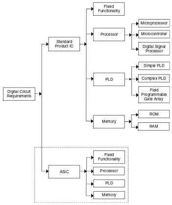
In the digital domain, the choice of implementation technology is essentially whether to use dedicated (and fixed) functionality digital logic, to use a software-programmed, processor-based system (designed based on a microprocessor,mP; microcontroller,mC; or digital signal processor, DSP), or to use a hardware-configured programmable logic device (PLD), whether simple (SPLD), complex (CPLD), or the field programmable gate array (FPGA). Memory used for the storage of data and program code is integral to many digital circuits and systems. The choices are shown in Figure 1.1.
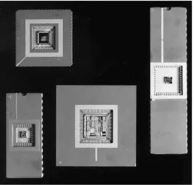
complexity of the circuit depending on the designed functionality. Examples of packaged ICs are shown in Figure 1.2.
In many circuits, the underlying technology will be based on IC, and a complete electronic circuit will consist of a number of ICs, together with other circuit
Digital Circuit Requirements
Standard Product IC
ASIC
PLD Fixed Functionality
Processor
Microprocessor
Microcontroller
Digital Signal Processor
Simple PLD
Complex PLD
Field Programmable
Gate Array
PLD Processor
Fixed Functionality
Memory Memory
ROM
RAM
Figure 1.1: Technology choices for digital circuit design
2 Chapter 1
components such as resistors and capacitors. In this book, the generic word technologywill be used throughout. TheOxford Dictionary of Englishdefines technologyas ‘‘the application of scientific knowledge for practical purposes, especially in industry’’ [1].
For us, this applies to the underlying electronic hardware and software that can be used to design a circuit for a given requirement. For the arrangement identified in Figure 1.1, a given set ofdigital circuit requirementsare developed, and the role of the designer is to come up with a solution that meets ideally all of the requirements. Typical requirements include:
• Cost restraints: The design process, the cost of components, the manufacturing costs, and the maintenance and future development costs must be within specific limits.
• Component supply: The designer might have a free hand in choosing the components to use, or restrictions may be set by the company or project management requirements.
• Prior experience: The designer may have prior experience in using a particular technology, which might or might not be suitable to the current design.
• Training: The designer might require specific training to utilize a specific technology if he or she does not have the necessary prior experience.
• Contract arrangements: If the design is to be created for a specific customer, the customer would typically provide a set of constraints that would be set down in the design contract.
• Size/volume constraints: the design would need to be manufactured to fit into a specific size/volume,
• Weight constraints: the design would need to be manufactured to be within specific weight restrictions (e.g. for portable applications such as mobile phones),
• Power source: the electronic product would be either fixed (in a single location so allowing for the use of a fixed power source) or portable (to be carried to multiple places requiring a portable power source (such as battery or solar cell),
• Power consumption constraints: The power consumption should be as low as possible in order to (i) minimise the power source requirements, (ii) be operable for a specific time on a limited power source, and (iii) be compatible with best practice in the development of electronic products that are conscious of environmental issues.
The initial choice for implementing the digital circuit is between a standard product IC and an ASIC (application-specific integrated circuit) [2]:
• Standard product IC: This is an off-the-shelf electronic component that has been designed and manufactured by a company for a given purpose, or range of use, and that is commercially available for others to use. These would be purchased either from a component supplier or directly from the designer or manufacturer.
• ASIC: This is an IC that has been specifically designed for an application. Rather than purchasing an off-the-shelf IC, the ASIC can be designed and manufactured to fulfil the design requirements.
4 Chapter 1
For many applications, developing an electronic system based on standard product ICs would be the approach taken as the time and costs associated with ASIC design, manufacture, and test can be substantial and outside the budget of a particular design project. Undertaking an ASIC design project also requires access to IC design experience and IC CAD tools, along with access to a suitable manufacturing and test capability. Whether a standard product IC or ASIC design approach is taken, the type of IC used or developed will be one of four types:
1. Fixed Functionality: These ICs have been designed to implement a specific functionality and cannot be changed. The designer would use a set of these ICs to implement a given overall circuit functionality. Changes to the circuit would require a complete redesign of the circuit and the use of different fixed functionality ICs.
2. Processor: The processor would be more familiar to the majority of people as it is in everyday use (the heart of the PC is a microprocessor). This component runs a software program to implement the required functionality. By
changing the software program, the processor will operate a different function. The choice of processor will depend on the microprocessor (mP), the microcontroller (mC), or the digital signal processor (DSP).
3. Memory: Memory will be used to store, provide access to, and allow modification of data and program code for use within a processor-based electronic circuit or system. The two basic types of memory are ROM (read-only memory) and RAM (random access memory). ROM is used for holding program code that must be retained when the memory power is removed. It is considered to providenonvolatile storage. The code can either be fixed when the memory is fabricated (mask programmable ROM) or electrically programmed once (PROM, Programmable ROM) or multiple times. Multiple programming capacity requires the ability to erase prior programming, which is available with EPROM (electrically programmable ROM, erased using ultraviolet [UV] light), EEPROM or E2PROM
to in the normal circuit application. However, flash memory can also be referred to as nonvolatile RAM (NVRAM). RAM is considered to provide a volatile storage, because unlike ROM, the contents of RAM will be lost when the power is removed. There are two main types of RAM: static RAM (SRAM) and dynamic RAM (DRAM).
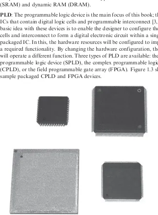
4. PLD: The programmable logic device is the main focus of this book; these are ICs that contain digital logic cells and programmable interconnect [3, 4]. The basic idea with these devices is to enable the designer to configure the logic cells and interconnect to form a digital electronic circuit within a single packaged IC. In this, the hardware resources will be configured to implement a required functionality. By changing the hardware configuration, the PLD will operate a different function. Three types of PLD are available: the simple programmable logic device (SPLD), the complex programmable logic device (CPLD), or the field programmable gate array (FPGA). Figure 1.3 shows sample packaged CPLD and FPGA devices.
Figure 1.3: Sample FPGA and CPLD packages
6 Chapter 1
Both the processor and PLD enable the designer to implement and change the functionality of the IC by changing either the software program or the hardware configuration. Because these two different approaches are easily confused, in this book the following terms will be used to differentiate the PLD from the processor:
• The PLD will be configured using a hardware configuration. • The processor will be programmed using a software program.
An ASIC can be designed to create any one of the four standard product IC forms (fixed functionality, processor, memory, or PLD). An ASIC would be designed in the same manner as a standard product IC, so anyone who has access to an ASIC design, fabrication, and test facility can create an equivalent to a standard product IC (given that patent and general legal issues around IP [intellectual property] considerations for existing designs and devices are taken into account). In addition, an ASIC might also incorporate a programmable logic fabric alongside the fixed logic hardware. Figure 1.1 shows what can be done with ASIC solution, but not how the ASIC would achieve this. Figure 1.4 shows the (i) four different forms of IC (i.e., what the IC does) that can be developed to emulate a standard product IC equivalent, and (ii) the three different design and implementation approaches.
In a full-custom approach, the designer would be in control of every aspect of ASIC design and layout—the way in which the electronic circuit is laid out on the die, which is the piece of rectangular or square material (usually silicon) onto
(i) What the ASIC does (ii) How the ASIC does it
ASIC Standard cell
Full custom
Mask programmable
gate array
Semi-custom ASIC
Memory Processor
Fixed Functionality
PLD
which the circuit components are manufactured. This would give the best circuit performance, but would be time consuming and expensive to undertake. Full-custom design is predominantly for analogue circuits and the creation of libraries of components for use in a semi-custom, standard cell design approach. An alternative to the full-custom approach uses a semi-custom approach. This is subdivided into a standard cell approach or mask programmable gate array
(MPGA) approach. The standard cell approach uses a library of predesigned basic circuit components (typically digital logic cells) that are connected within the IC to form the overall circuit. In a simplistic view, this would be similar to creating a design by connecting fixed functionality ICs together, but instead of using multiple ICs, a single IC is created. This approach is faster and lower cost than afull-custom approach but would not necessarily provide the best circuit performance. Because only the circuits required within the design would be manufactured (fabricated), there would be an immediate trade-off between circuit performance, design time, and design cost (a trade-off that is encountered on a daily basis by the designer). The MPGA approach is similar to a standard cell approach in that a library of components is available and connected, but the layout on the (silicon) die is different. An array of logic gates is predetermined, and the circuit is created by creating metal interconnect tracks between the logic gates. In the MPGA approach, not necessarily all of the logic gates fabricated on the die would be used. This would use a larger die than in a standard cell approach, with the inclusion of unused gates, but it has the advantage of being faster to fabricate than a standard cell approach.
A complement to the ASIC is thestructured ASIC[16, 17]. Thestructured ASICis seen to offer a promising alternative to standard cell ASICs and FPGAs for the mid and high volume market.Structured ASICsare similar to the mask programmable gate array in that they have customisable metal interconnect layers patterned on top of a prefabricated base. Either standard logic gates or look-up tables (LUTs) are fabricated in a 2-dimensional array that forms the underlying pattern of logic gates, memory, processors and IP blocks. This base is programmed using a small number of metal masks. The purpose of this is to reduce the non-recurring engineering (NRE) costs when compared to a standard cell ASIC approach and to bridge the gap that exists between the standard cell ASIC and FPGA where:
1. Standard cell ASICs provide support for large, complex designs with high performance, low cost per unit (if produced in volume), but at the cost of long
8 Chapter 1
development times, high NRE costs and long fabrication times when implementing design modifications,
2. FPGAs provide for short development times, low NRE costs and short times to implement design modifications, but at the cost of limited design
complexities, performance limitations and high cost per unit.
NRE cost reductions using Structured ASICs are considered with a reduction in manufacturing costs and reducing the design tasks. They can also offer mixed-signal circuit capability, a potential advantage when compared to digital only FPGAs.
Hardware configured devices (i.e., PLDs) are becoming increasingly popular because of their potential benefits in terms of logic replacement potential
(obsolescence), rapid prototyping capabilities, and design speed benefits in which PLD-based hardware can implement the same functions as a software-programmed, processor-based system, but in less time. This is particularly important for
computationally expensive mathematical operations such as the fast Fourier transform (FFT) [5].
The aim of this book is to provide a reference text for students and practicing engineers involved in digital electronic circuit and systems design using PLDs. The PLD is digital in nature and this type of device will be the focus of the book. However, it should also be noted that mixed-signal programmable devices have also been developed and are available for use within mixed-signal circuits that require programmable analogue circuit (e.g. programmable analogue amplifier)
components. Whilst this technology is not covered in this book, the reader is recommended to undertake their own research activities to (i) identify the programmable mixed-signal devices currently available (such as the Lattice Semiconductor Corporation ispPAC and AnadigmTMFPAA (Field Programmable Analog Array)), and also (ii) the history of programmable mixed-signal and devices that have been available in the past but no longer available. The text will introduce the basic concepts of programmable logic, along with case study designs in a range of electronic systems that target signal generation and data acquisition systems for a variety of applications from control and instrumentation through test equipment systems. To achieve this, a range of FPGA and CPLD device types will be
1.2
Electronic Circuits: Analogue and Digital
1.2.1
Introduction
Before looking into detail of what the PLD is and how to use it, it is important to identify that the PLD is digital in nature, and digital circuits and signals are different from analogue circuits and signals. This section will provide an overview of the main characteristics and differences between the continuous- and discrete-time, and the analogue and digital, worlds.
1.2.2
Continuous Time versus Discrete Time
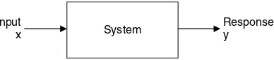
Electronic circuits will receive electrical signals (voltages and/or currents) and modify these to produce a response, which will be a voltage and/or current that is a modified version of the input signal (see Figure 1.5). The signal will be electrical in nature and will convey information concerning the behavior of the related system. Theinputto the systemwill typically be created by a variation of a measurable quantity by the use of a suitable sensor. Theresponsewill be a modified version of the input that is in a form that can be used. In Figure 1.5, an electronic system receives an input,x, and produces a response (output),y. The system implements a certain function that is designed to undertake an operation that is of a particular use within the context of the overall system. Here, the system receives a single input and produces a single response. The term systemis another generic term which is defined in theOxford Dictionary of Englishas ‘‘a set of things working together as parts of a mechanism or an interconnecting network’’ [1].
For us, this applies to the overall set of electronic components and software programs that work together to perform the particular set of requirements. In general, there may be one or more inputs and one or more outputs. The system is shown as ablack boxin that the details of its internal operation are hidden and only theinput-output relationship is known. This black box creates asignal processor, and the designer is tasked with
System Input
x
Response y
Figure 1.5: Electronic system block diagram
10 Chapter 1
creating the internal details using a suitable electronic circuit technology. The input-output relationship will normally be modeled by a suitable mathematical algorithm. The type of signal [6, 7] that the signal processor accepts and responds to will vary in time but will be classified as either a continuous-time or a discrete-time signal.
Acontinuous-time signalcan be represented mathematically as a function of a continuous-time variable. The signal varies in time but is also continuous in time. Figure 1.6 provides four examples of continuous-time signals: (i) a constant value, (ii) a sine wave, (iii) a square wave, and (iv) an arbitrary waveform. Waveforms (i), (ii), and (iv) are continuous in both time and amplitude; (iii) is continuous in time but discontinuous in amplitude. All signals are classified as continuous-time signals.
Adiscrete-time signalis defined only by values at set points in time, referred to as the sampling instants. It is normal to set the time spacing between the sampling instants to a fixed value, T, referred to as thesampling interval. Thesampling frequencyis fS= 1/T,
where T is seconds and fSis Hertz (Hz). When a signal is sampled at a fixed rate, this
is referred to asperiodic sampling. Figure 1.7 provides examples of discrete-time signals that are sampled values of the continuous time signals shown in Figure 1.6.
When a discrete-time signal is expressed, it will normally be expressed by the sample number (n) wheren =0 denotes the first sample,n = pdenotes thepthsample, and nincrements in steps of 1. For a signalx, then, the samples will be x[0], x[1], x[2], x[3], . . . ,x[p]. A discrete-time signal would represent a sampled analogue signal. Hence, an electronic circuit would have continuous-time or discrete-time inputs and continuous-time or discrete-time outputs as represented in Table 1.1.
time (t)
time (t) time (t)
(i) Constant
(iii) Square wave
(ii) Sine wave
(iv) Arbitrary waveform time (t)
1.2.3
Analogue versus Digital
The electronic system as shown in Figure 1.8 will perform its operations on signals that are either analogue or digital in nature, using either analogue or digital electronic circuits. Hence, a signal may be of one of two types, analogue or digital.
Ananalogue signalis a continuous- or discrete-time signal whose amplitude is continuous in value between a lower and upper limit, but may be either a continuous time or discrete time.
Table 1.1: Signal types (continuous- and discrete-time)
Input signal type Response signal type Continuous-time ! Continuous-time Continuous-time ! Discrete-time Discrete-time ! Discrete-time
Discrete-time ! Continuous-time
(i) Constant
(iii) Square wave
(ii) Sine wave
(iv) Arbitrary waveform time (t)
time (t)
time (t)
time (t)
Amplitude Amplitude
Amplitude Amplitude
Figure 1.7: Examples of discrete-time signals
System Input
x
Response y
Figure 1.8: Electronic system block diagram
12 Chapter 1
Adigital signalis a continuous or discrete-time signal with discrete values between a lower and upper limit. These discrete values will be represented by numerical values and be in a form suitable fordigital signal processing. If the discrete-time signal has been derived from a continuous-time signal by sampling, then the sampled signal is converted into a digital signal byquantization, which produces a finite number of values from a continuous amplitude signal. It is common to use the binary number (i.e., two values, 0 or 1) system to represent a number in a digital representation. An electronic circuit would have analogue or digital inputs and analogue or digital outputs as represented in Table 1.2. When an analogue signal is sampled and
converted to digital, this is undertaken using an analogue-to-digital converter (ADC) [8]. When a digital signal is converted back to analogue, this is undertaken using a digital-to-analogue converter (DAC).
An example of both analogue and digital signals and circuits is shown in Figure 1.9. This electronic temperature controller, as might be used in a home
Table 1.2: Signal types (analogue and digital)
Input signal type Response signal type
Analogue ! Analogue
Analogue ! Digital
Digital ! Digital
Digital ! Analogue
Sensor Sensor signal
conditioning circuit
Analogue-to-Digital Converter
Temperature Digital
signal processing
Digital-to-Analogue Converter Controller Signal conditioningcircuit
Heat
Analogue Analogue Analogue Digital
Digital Analogue
Analogue Analogue
heating system, uses digital signal processing. The system is shown as a block diagram in which each block represents a major operation. In a design each block would be represented by its ownblock diagram, going into evermore detail until the underlying circuit hardware (and software) details are identified. The block diagram provides a convenient way to represent the major system operations called a top-down design approach, starting at a high level of design abstraction (initially independent of the final design implementation details) and working down to the final design implementation details.
Here, the room temperature is sensed as an analogue signal, but must be processed by a digital signal processing circuit, so it must be sensed and converted to an analogue voltage or current. This is then applied to a sensor signal conditioning circuit that is used to connect the sensor to the ADC. The ADC samples the analogue signal at a chosen sampling frequency. Once a temperature sample has been obtained by the digital signal processing circuit, it is then processed using a particular algorithm, and the result is applied to a DAC. The DAC output is a voltage or current that is used to drive a controller (heat source). The DAC is normally connected to the controller via a signal conditioning circuit. This circuit acts to interface the DAC to the controller in order for the controller to receive the correct voltage and current levels. This particular system is also an example of a closed-loop control system using an electronic controller. The control system is generalized as shown in Figure 1.10 [9, 10].
1.3
History of Digital Logic
Early electronic circuits were analogue, and before the advent of digital logic, signal processing was undertaken using analogue electronic circuits. The
invention of the semiconductor transistor in 1947 at Bell Laboratories [11] and
Controller Plant Plant output(heat)
+
Temperature Sensor
–
Required temperature
Figure 1.10: General control system
14 Chapter 1
the improvements in transistor characteristics and fabrication during the 1950s led to the introduction of linear (analogue) ICs and the first transistor-transistor logic (TTL) digital logic IC in the early 1960s, closely followed by complementary metal oxide semiconductor (CMOS) ICs. The early devices incorporated a small number of logic gates. However, rapid growth in the ability to fabricate an increasing number of logic gates in a single IC led to the microprocessor in the early 1970s. This, with the ability to create memory ICs with ever increasing capacities, laid the foundation for the rapid expansion in the computer industry and the types of complex digital systems based on the computer architecture that we have available today. The last fifty years have seen a revolution in the electronics industry.
Fundamentally, a digital circuit will be categorized into one of three general types, each of which is created and fabricated within an integrated circuit:
• Combinational logic, in which the response of the circuit is based on a Boolean logic expression of the input only and the circuit responds immediately to a change in the input.
• Sequential logic, in which the response of the circuit is based on the current state of the circuit and the sometimes the current input. This may be
asynchronousorsynchronous. Insynchronous sequential logic, the logic changes state whenever an externalclockcontrol signal is applied. Inasynchronous sequential logic, the logic changes state on changes of the input data (the circuit does not utilize aclockcontrol signal).
• Memory, in which digital values can be stored and retrieved some time later. For a user, memory can be eitherread-only(ROM) orrandom-access(RAM). In ROM, the data stored in the memory are initially placed in the memory and can only be read by the user. Data cannot normally be altered in the
circuit application. In RAM (also referred to asread-write memory, RWM), the user can write data to the memory and read the data back from the memory.
The digital IC consists of a number of logic gates, which are combinational or sequential circuit elements. The logic gates may be implemented using different fabrication processes and different circuit architectures:
• CMOS, complementary metal oxide semiconductor
• BiCMOS, bipolar and CMOS
The material predominantly used to fabricate the digital logic circuits is silicon. However, silicon-based circuits are complemented with the digital logic capabilities of circuits fabricated using gallium arsenide (GaAs) and silicon germanium (SiGe) technologies. Today, silicon-based CMOS is by far the dominant process used for digital logic.
The digital logic gate is actually an abstraction of what is happening within the underlying circuit. All digital logic gates are made up of transistors. The logic gates may take one of a number of different circuit architectures (the way in which the transistors are interconnected) at the transistor level:
• static CMOS
• dynamic CMOS
• pass transistor logic CMOS
Today, static CMOS logic is by far the dominant logic cell design structure used. The number of logic gates within a digital logic IC will range from a few to hundreds of thousands and ultimately millions for the more complex processors and PLDs. In previous times, when the potential for higher levels of integration was far less than is now possible, the digital IC was classified by the level of integration—that is, the number of logic gate equivalents per IC (see Table 1.3). With increasing levels of integration, the following levels were identified as follow-on descriptions from VLSI, but these are not in common usage:
• ULSI, ultra-large-scale integration
• WSI, wafer scale integration
Table 1.3: Levels of integration
Level of integration Acronym Number of gate equivalents per IC Small-scale integration SSI <10
Medium-scale integration MSI 10–100
Large-scale integration LSI 100–10,000
Very large-scale integration VLSI >10,000
16 Chapter 1