Thermal-Aware
Thermal-Aware
Testing of Digital VLSI
Circuits and Systems
6000 Broken Sound Parkway NW, Suite 300 Boca Raton, FL 33487-2742
© 2018 by Taylor & Francis Group, LLC
CRC Press is an imprint of Taylor & Francis Group, an Informa business
No claim to original U.S. Government works
Printed on acid-free paper
International Standard Book Number-13: 978-0-8153-7882-2 (Hardback)
This book contains information obtained from authentic and highly regarded sources. Reasonable efforts have been made to publish reliable data and information, but the author and publisher cannot assume responsibility for the validity of all materials or the consequences of their use. The authors and publishers have attempted to trace the copyright holders of all material reproduced in this publication and apologize to copyright holders if permission to publish in this form has not been obtained. If any copyright material has not been acknowledged please write and let us know so we may rectify in any future reprint.
Except as permitted under U.S. Copyright Law, no part of this book may be reprinted, reproduced, transmitted, or utilized in any form by any electronic, mechanical, or other means, now known or hereafter invented, including photocopying, microfilming, and recording, or in any information storage or retrieval system, without written permission from the publishers.
For permission to photocopy or use material electronically from this work, please access
www.copyright.com (http://www.copyright.com/) or contact the Copyright Clearance Center, Inc. (CCC), 222 Rosewood Drive, Danvers, MA 01923, 978-750-8400. CCC is a not-for-profit organization that provides licenses and registration for a variety of users. For organizations that have been granted a photocopy license by the CCC, a separate system of payment has been arranged.
Trademark Notice: Product or corporate names may be trademarks or registered trade-marks, and are used only for identification and explanation without intent to infringe.
Library of Congress Cataloging-in-Publication Data Names: Chattopadhyay, Santanu, author.
Title: Thermal-aware testing of digital VLSI circuits and systems / Santanu Chattopadhyay.
Description: First edition. | Boca Raton, FL : Taylor & Francis Group, CRC Press, 2018. | Includes bibliographical references and index. Identifiers: LCCN 2018002053| ISBN 9780815378822 (hardback : acid-free paper) | ISBN 9781351227780 (ebook)
Subjects: LCSH: Integrated circuits--Very large scale integration--Testing. | Digital integrated circuits--Testing. | Integrated circuits--Very large scale integration--Thermal properties. | Temperature measurements. Classification: LCC TK7874.75 .C464 2018 | DDC 621.39/50287--dc23 LC record available at https://lccn.loc.gov/2018002053
Visit the Taylor & Francis Web site at http://www.taylorandfrancis.com
To
SANTANA, MY WIFE
My Inspiration
and
SAYANTAN, OUR SON
vii
Contents
List of Abbreviations,
xi
Preface,
xiii
Acknowledgments,
xvii
Author,
xix
CHAPTER 1
◾VLSI Testing: An Introduction
1
1.1 TESTING IN THE VLSI DESIGN PROCESS 2
1.2 FAULT MODELS 5
1.2.1 Stuck-at Fault Model 6
1.2.2 Transistor Fault Model 6
1.2.3 Bridging Fault Model 7
1.2.4 Delay Fault Model 7
1.3 TEST GENERATION 8
1.3.1 D Algorithm 8
1.4 DESIGN FOR TESTABILITY (DFT) 10
1.4.1 Scan Design—A Structured DFT Approach 11
1.4.2 Logic Built-In Self Test (BIST) 14
1.5 POWER DISSIPATION DURING TESTING 16
1.5.1 Power Concerns During Testing 17
1.7 THERMAL MODEL 21
1.8 SUMMARY 24
REFERENCES 24
CHAPTER 2
◾Circuit-Level Testing
25
2.1 INTRODUCTION 25
2.2 TEST-VECTOR REORDERING 27
2.2.1 Hamming Distance-Based Reordering 28
2.2.2 Particle Swarm Optimization-Based
Reordering 31
2.3 DON’T CARE FILLING 39
2.3.1 Power and Thermal Estimation 41
2.3.2 Flip-Select Filling 42
2.4 SCAN-CELL OPTIMIZATION 44
2.5 BUILT-IN SELF TEST 47
2.5.1 PSO-based Low Temperature LT-RTPG
Design 49
2.6 SUMMARY 50
REFERENCES 51
CHAPTER 3
◾Test-Data Compression
53
3.1 INTRODUCTION 53
3.2 DICTIONARY-BASED TEST DATA
COMPRESSION 55
3.3 DICTIONARY CONSTRUCTION USING
CLIQUE PARTITIONING 56
3.4 PEAK TEMPERATURE AND COMPRESSION
TRADE-OFF 59
3.5 TEMPERATURE REDUCTION WITHOUT
Contents ◾ ix
3.6 SUMMARY 69
REFERENCES 69
CHAPTER 4
◾System-on-Chip Testing
71
4.1 INTRODUCTION 71
4.2 SOC TEST PROBLEM 72
4.3 SUPERPOSITION PRINCIPLE-BASED
THERMAL MODEL 74
4.4 TEST SCHEDULING STRATEGY 78
4.4.1 Phase I 79
4.4.2 Phase II 85
4.4.2.1 PSO Formulation 85
4.4.2.2 Particle Fitness Calculation 86
4.5 EXPERIMENTAL RESULTS 90
4.6 SUMMARY 92
REFERENCES 94
CHAPTER 5
◾Network-on-Chip Testing
95
5.1 INTRODUCTION 95
5.2 PROBLEM STATEMENT 98
5.3 TEST TIME OF NOC 99
5.4 PEAK TEMPERATURE OF NOC 100
5.5 PSO FORMULATION FOR PREEMPTIVE
TEST SCHEDULING 101
5.6 AUGMENTATION TO THE BASIC PSO 103
5.7 OVERALL ALGORITHM 104
5.8 EXPERIMENTAL RESULTS 106
5.8.1 Effect of Augmentation to the Basic PSO 106
5.8.3 Thermal-Aware Test Scheduling Results 107
5.9 SUMMARY 107
REFERENCES 109
xi
List of Abbreviations
3D Three dimensional
ATE Automatic Test Equipment
ATPG Automatic Test Pattern Generation BIST Built-In Self Test
CAD Computer-Aided Design CLK Clock Signal
CTM Compact Thermal Model CUT Circuit Under Test DFT Design for Testability
DI Data Input
DPSO Discrete Particle Swarm Optimization FEM Finite Element Method
IC Integrated Circuit IP Intellectual Property
LFSR Linear Feedback Shift Register
LT-RTPG Low Transition-Random Test Pattern Generator MISR Multiple-Input Signature Register
MTTF Mean Time to Failure NoC Network-on-Chip NTC Node Transit Count ORA Output-Response Analyzer PCB Printed Circuit Board PSO Particle Swarm Optimization SE Scan Enable
xiii
Preface
scheduling of core tests and test-data compression in System-on-Chip (SoC) and Network-System-on-Chip (NoC) designs. This book highlights the research activities in the domain of thermal-aware testing. Thus, this book is suitable for researchers working on power- and thermal-aware design and testing of digital very large scale integration (VLSI) chips.
Organization: The book has been organized into five chapters.
A summary of the chapters is presented below.
Chapter 1, titled “VLSI Testing—An Introduction,” introduces the topic of VLSI testing. The discussion includes importance of testing in the VLSI design cycle, fault models, test-generation techniques, and design-for-testability (DFT) strategies. This has been followed by the sources of power dissipation during testing and its effects on the chip being tested. The problem of thermal-aware testing has been enumerated, clearly bringing out the limitations of power-constrained test strategies in reducing peak temperature and its variance. The thermal model used in estimating temperature values has been elaborated.
Chapter 2, “Circuit Level Testing,” notes various circuit-level techniques to reduce temperature. Reordering the test vectors has been shown to be a potential avenue to reduce temperature. As test-pattern generation tools leave large numbers of bits as don’t cares, they can be filled up conveniently to aid in temperature reduction. Usage of different types of flip-flops in the scan chains can limit the activities in different portions of the circuit, thus reducing the heat generation. Built-in self-test (BIST) strategies use an on-chip test-pattern generator (TPG) and response analyzer. These modules can be tuned to get a better temperature profile. Associated techniques, along with experimental results, are presented in this chapter.
Preface ◾ xv
of compression and the attained reduction in temperature. This chapter presents techniques for dictionary-based compression, temperature-compression trade-off, and temperature reduction techniques without sacrificing on the compression.
Chapter 4, titled “System-on-Chip Testing,” discusses system-level temperature minimization that can be attained via scheduling the tests of various constituent modules in a system-on-chip (SoC). The principle of superposition is utilized to get the combined effect of heating from different sources onto a particular module. Test scheduling algorithms have been reported based on the superposition principle.
Chapter 5, titled as “Network-on-Chip Testing,” discusses thermal-aware testing problems for a special variant of system-on-chip (SoC), called network-on-system-on-chip (NoC). NoC contains within it a message transport framework between the modules. The framework can also be used to transport test data. Optimization algorithms have been reported for the thermal-aware test scheduling problem for NoC.
Santanu Chattopadhyay
xvii
Acknowledgments
I
must acknowledge the contribution of my teachers who taught me subjects such as Digital Logic, VLSI Design, VLSI Testing, and so forth. Clear discussions in those classes helped me to consolidate my knowledge in these domains and combine them properly in carrying out further research works in digital VLSI testing. I am indebted to the Department of Electronics and Information Technology, Ministry of Communications and Information Technology, Government of India, for funding me for several research projects in the domain of power- and thermal-aware testing. The works reported in this book are the outcome of these research projects. I am thankful to the members of the review committees of those projects whose critical inputs have led to the success in this research work. I also acknowledge the contribution of my project scholars, Rajit, Kanchan, and many others in the process.My source of inspiration for writing this book is my wife Santana, whose relentless wish and pressure has forced me to bring the book to its current shape. Over this long period, she has sacrificed a lot on the family front to allow me to have time to continue writing, taking all other responsibilities onto herself. My son, Sayantan always encouraged me to write the book.
I also hereby acknowledge the contributions of the publisher, CRC Press, and its editorial and production teams for providing me the necessary support to see my thoughts in the form of a book.
xix
Author
Santanu Chattopadhyay received a BE degree in Computer Science and Technology from Calcutta University (BE College), Kolkata, India, in 1990. In 1992 and 1996, he received an MTech in computer and information technology and a PhD in computer science and engineering, respectively, both from the Indian Institute of Technology, Kharagpur, India. He is currently a professor in the Electronics and Electrical Communication Engineering Department, Indian Institute of Technology, Kharagpur. His research interests include low-power digital circuit design and testing, System-on-Chip testing, Network-on-Chip design and testing, and logic encryption. He has more than one hundred publications in international journals and conferences. He is a co-author of the book Additive Cellular Automata—Theory
and Applications, published by the IEEE Computer Society Press.
He has also co-authored the book titled Network-on-Chip: The
Next Generation of System-on-Chip Integration, published by
the CRC Press. He has written a number of text books, such as
Compiler Design, System Software, and Embedded System Design,
1 C H A P T E R
1
VLSI Testing
An Introduction
process, a large number of chips are produced on the same silicon wafer. This reduces the cost of production for individual chips, but each chip needs to be tested separately—checking one of the lot does not give the guarantee of correctness for the others. Testing is necessary at other stages of the manufacturing process as well. For example, an electronic system consists of printed circuit boards
(PCBs). IC chips are mounted on PCBs and interconnected via metal lines. In the system design process, the rule of ten says that the cost of detecting a faulty IC increases by an order of magnitude as it progresses through each stage of the manufacturing process— device to board to system to field operation. This makes testing a very important operation to be carried out at each stage of the manufacturing process. Testing also aids in improving process yield by analyzing the cause of defects when faults are encountered. Electronic equipment, particularly that used in safety-critical applications (such as medical electronics), often requires periodic testing. This ensures fault-free operation of such systems and helps to initiate repair procedures when faults are detected. Thus, VLSI testing is essential for designers, product engineers, test engineers, managers, manufacturers, and also end users.
The rest of the chapter is organized as follows. Section 1.1 presents the position of testing in the VLSI design process. Section 1.2 introduces commonly used fault models. Section 1.3 enumerates the deterministic test-generation process. Section 1.4 discusses design for testability (DFT) techniques. Section 1.5 presents the sources of power dissipation during testing and associated concerns. Section 1.6 enumerates the effects of high temperature in ICs. Section 1.7 presents the thermal model. Section 1.8 summarizes the contents of this chapter.
1.1 TESTING IN THE VLSI DESIGN PROCESS
VLSI Testing ◾ 3
the other hand, circuits that fail to produce correct responses for any of the test patterns are assumed to be faulty. Testing is carried out at different stages of the life cycle of a VLSI device.
Typically, the VLSI development process goes through the following stages in sequence: design, fabrication, packaging, and quality assurance. It starts with the specification of the system. Designers convert the specification into a VLSI design. The design is verified against the set of desired properties of the envisaged application. The verification process can catch the design errors, which are subsequently rectified by the designers by refining their design. Once verified and found to be correct, the design goes into fabrication. Simultaneously, the test engineers develop the test plan based upon the design specification and the fault model associated with the technology. As noted earlier, because of unavoidable statistical flaws in the silicon wafer and masks, it is impossible to guarantee 100% correctness in the fabrication process. Thus, the ICs fabricated on the wafer need to be tested to separate out the defective devices. This is commonly known as wafer-level testing. This test process needs to be very cautious as the bare-minimum die cannot sustain high power and temperature values. The chips passing the wafer-level test are packaged. Packaged ICs need to be tested again to eliminate any devices that were damaged in the packaging process. Final testing is needed to ensure the quality of the product before it goes to market; it tests for parameters such as timing specification, operating voltage, and current. Burn-in or stress testing is performed in which the chips are subjected to extreme conditions, such as high supply voltage, high operating temperature, etc. The burn-in process accelerates the effect of defects that have the potential to lead to the failure of the IC in the early stages of its operation.
The quality of a manufacturing process is identified by a quantity called yield, which is defined as the percentage of acceptable parts among the fabricated ones.
Yield Parts accepted Parts fabricated
Yield may be low because of two reasons: random defects and process variations. Random defects get reduced with improvements
in computer aided design (CAD) tools and the VLSI fabrication
process. Hence, parametric variations due to process fluctuation become the major source of yield loss.
Two undesirable situations in IC testing may occur because of the poorly designed test plan or the lack of adherence to the design for testability (DFT) policy. The first situation is one in which a faulty device appears to be good and passes the test, while in the second case, a good chip fails the test and appears to be faulty. The second case directly affects the yield, whereas the first one is more serious because those faulty chips are finally going to be rejected during the field deployment and operation. Reject rate is defined as the ratio of field-rejected parts to all parts passing the quality test.
Reject rate Faulty parts passing final test Total number of part
= ( )
( ss passing final test)
VLSI Testing ◾ 5
may not ensure the testing of the circuit in all its states. Further, with the increase in the value of n, the size of the test-pattern set increases exponentially.
Another mode of testing, called structural testing, uses the structural information of the CUT and a fault model. A fault model, discussed later, abstracts the physical defects in the circuit into different types of faults. Test vectors are generated targeting different types of faults in the circuit elements—gates, transistors, flip-flops, and signal lines. A quantitative measure about the quality of a test-pattern set corresponding to a fault model is expressed as fault coverage. Fault coverage of a test-pattern set for a circuit with respect to a fault model is defined as the ratio of the number of faults detected by the test set to the total number of modeled faults in the circuit. However, for a circuit, all faults may not be detectable. For such an undetectable fault, no pattern exists that can produce two different outputs from the faulty and fault-free circuits. Determining undetectable faults for a circuit is itself a difficult task. Effective fault coverage is defined as the ratio of the number of detected faults to the total number of faults less the number of undetectable faults. Defect level is defined as,
Defect level=1−yield(1−fault coverage).
Improving fault coverage improves defect level. Since enhancing yield may be costly, it is desirable to have test sets with high fault coverage.
1.2 FAULT MODELS
As the types of defects in a VLSI chip can be numerous, it is necessary to abstract them in terms of some faults. Such a fault model should have the following properties:
2. Be computationally efficient to generate test patterns for the model faults and to perform fault simulation for evaluating the fault coverage.
Many fault models have been proposed in the literature; however, none of them can comprehensively cover all types of defects in VLSI chips. In the following, the most important and widely used models have been enumerated.
1.2.1 Stuck-at Fault Model
A stuck-at fault affects the signal lines in a circuit such that a line has its logic value permanently as 1 (stuck-at-one fault) or 0 (stuck-at-zero fault), irrespective of the input driving the line. For example, the output of a 2-input AND-gate may be stuck-at 1. Even if one of the inputs of the AND-gate is set to zero, the output remains at 1 only. A stuck-at fault transforms the correct value on the faulty signal line to appear to be stuck at a constant logic value, either 0 or 1. A single stuck-at fault model assumes that only one signal line in the circuit is faulty. On the other hand, a more generic multiple stuck-at fault model assumes multiple lines become faulty simultaneously. If there are n signal lines in the circuit, in a single stuck-at fault model, the probable number of faults is 2n. For a multiple stuck-at fault model, the total number of faults becomes 3n−1 (each line can be in one of the three states—
fault free, stuck-at 1, or stuck-at 0). As a result, multiple stuck-at fault is a costly proposition as far as test generation is concerned. Also, it has been observed that test patterns generated assuming a single stuck-at fault model are often good enough to identify circuits with multiple stuck-at faults also (to be faulty).
1.2.2 Transistor Fault Model
VLSI Testing ◾ 7
gate if one or more transistors inside the gate are open or short. Detecting a stuck-open fault often requires a sequence of patterns to be applied to the gate inputs. On the other hand, stuck-short faults are generally detected by measuring the current drawn from the power supply in the steady-state condition of gate inputs. This is more commonly known as IDDQ testing.
1.2.3 Bridging Fault Model
When two signal lines are shorted due to a defect in the manufacturing process, it is modeled as a bridging fault between the two. Popular bridging fault models are wired-AND and
wired-OR. In the wired-AND model, the signal net formed by the
two shorted lines take the value, logic 0, if either of the lines are at logic 0. Similarly, in the Wired-OR model, the signal net gets the value equal to the logical OR of the two shorted lines. These two models were originally proposed for bipolar technology, and thus not accurate enough for CMOS devices. Bridging faults for CMOS devices are dominant-AND and dominant-OR. Here, one driver dominates the logic value of the shorted nets, but only for a given logic value.
1.2.4 Delay Fault Model
A delay fault causes excessive delay along one or more paths in
the circuit. The circuit remains functionally correct, only its delay increases significantly. The most common delay fault model is the
path delay fault. It considers the cumulative propagation delay of a signal through the path. It is equal to the sum of all gate delays along the path. The major problem with path delay faults is the existence of a large number of paths through a circuit. The number can even be exponential to the number of gates, in the worst case. This makes it impossible to enumerate all path delay faults for test generation and fault simulation. Delay faults require an ordered pair of test vectors <v1,v2> to be applied to the circuit inputs.
The first vector v1 sensitizes the path from input to output, while
presence of a delay fault, the transition at output gets delayed from its stipulated time. A high-speed, high-precision tester can detect this delay in the transition.
1.3 TEST GENERATION
Test-pattern generation is the task of producing test vectors to ensure high fault coverage for the circuit under test. The problem is commonly referred to as automatic test-pattern generation (ATPG). For deterministic testing, test patterns generated by ATPG tools are stored in the automatic-test equipment (ATE). During testing, patterns from ATE are applied to the circuit and the responses are collected. ATE compares the responses with the corresponding fault-free ones and accordingly declares the circuit to have passed or failed in testing. The faulty responses can lead the test engineer to predict the fault sources, which in turn may aid in the diagnosis of defects.
Many ATPG algorithms have been proposed in the literature. There are two main tasks in any ATPG algorithm: exciting the target fault and propagating the fault effect to a primary output. A five-valued algebra with possible logic values of 0, 1, X, D, and D has been proposed for the same. Here, 0, 1, and X are the conventional logic values of true, false, and don’t care. D represents a composite logic value 1/0 and D represents 0/1. Logic operations involving
D are carried out component-wise. Considering, in this composite notation, logic-1 is represented as 1/1 and D as 1/0, “1 AND D” is equal to 1/1 AND 1/0 = (1 AND 1)/(1 AND 0) = 1/0 =D. Also, “D OR D” is equal to 1/0 OR 0/1 = (1 OR 0)/(0 OR 1) = 1/1 = 1. NOT(D) = NOT(1/0) = NOT(1)/NOT(0) = 0/1 = D.
1.3.1 D Algorithm
This is one of the most well-known ATPG algorithms. As evident from the name of the algorithm, it tries to propagate a D or D
of the target fault to a primary output. To start with, two sets,
VLSI Testing ◾ 9
D-frontier: This is the set of gates whose output value is X and one or more inputs are at value D or D. To start with, for a target fault f, D algorithm places a D or D at the fault location. All other signals are at X. Thus, initially, D-frontier contains all gates that are successors of the line corresponding to the fault f.
J-frontier: It is the set of circuit gates with known output values but not justified yet by the inputs. To detect a fault f, all gates in
J-frontier need to be justified.
The D algorithm begins by trying to propagate the D (or D) at the fault site to one of the primary outputs. Accordingly, gates are added to the D-frontier. As the D value is propagated, D-frontier
eventually becomes the gate corresponding to the primary output. After a D or D has reached a primary output, justification for gates in J-frontier starts. For this, J-frontier is advanced backward by placing the predecessors of gates in current J-frontier and justifying them. If a conflict occurs in the process, backtracking is invoked to try other alternatives. The process has been enumerated
in Algorithm D-Algorithm noted next.
Algorithm D-Algorithm
Input: C, the circuit under test.
f, the target fault.
Output: Test pattern if the f is testable, else the declaration “untestable.”
Begin
Step 1: Set all circuit lines to X.
Step 2: Set line corresponding to f to D or D; add it to D-frontier. Step 3: Set J-frontier to NULL.
Step 4: Set pattern_found to Recursive_D(C).
Step 5: If pattern_found then print the primary input values, else print “untestable.”
Procedure Recursive_D(C) begin
If conflict detected at circuit line values or D-frontier empty, return false;
If fault effect not reached any primary output then While all gates in D-frontier not tried do begin
Let g be an untried gate;
Set all unassigned inputs of g to non-controlling values and add them to J-frontier;
pattern_found=Recursive_D(C);
If pattern_found return “TRUE”;
end;
If J-frontier is empty return “TRUE”;
Let g be a gate in J-frontier; While g is not justified do
begin
Let k be an unassigned input of g; Set k to 1 and insert k= 1 to J-frontier;
pattern_found=Recursive_D(C);
If pattern_found return “TRUE”, else set k=0;
end;
Return “FALSE”; end.
1.4 DESIGN FOR TESTABILITY (DFT)
VLSI Testing ◾ 11
the effort involved in transferring the fault effect to any primary output is the observability measure of the point. Depending upon the complexity of the design, these controllability and observability metrics for the circuit lines may be poor. As a result, the test-generation algorithms may not be able to come up with test sets having high fault coverage. The situation is more difficult for sequential circuits, as setting a sequential circuit to a required internal state may necessitate a large sequence of inputs to be applied to the circuit. Design for testability (DFT) techniques attempt to enhance the controllability and observability of circuit lines to aid in the test-generation process. The DFT approaches can be broadly classified into ad hoc and structural approaches.
Ad hoc DFT approach suggests adherence to good design practices. The following are a few examples of the same:
• Inserting test points
• Avoiding asynchronous reset for flip-flops
• Avoiding combinational feedback loops
• Avoiding redundant and asynchronous logic
• Partitioning a big circuit into smaller ones
1.4.1 Scan Design—A Structured DFT Approach
Scan design is the most widely used DFT technique that aims at improving the controllability and observability of flip-flops in a sequential design. The sequential design is converted into a scan design with three distinct modes of operation: normal mode,
shift mode, and capture mode. In normal mode, the test signals
are deactivated. As a result, the circuit operates in its normal functional mode. In the shift and capture modes, a test mode
Figure 1.1a shows a sequential circuit with three flip-flops. For testing some fault in the combinational part of the circuit, the test-pattern generator may need some of the pseudo-primary inputs to be set to some specific values over and above the primary inputs. Thus, it is necessary to put the sequential circuit into some specific state. Starting from the initial state of the sequential circuit, it may be quite cumbersome (if not impossible) to arrive at such a configuration. The structure is modified, as shown in Figure 1.1b, in which each flip-flop is replaced by a muxed-D scan cell. Each such cell has inputs like data input (DI), scan input (SI), scan enable (SE), and clock signal (CLK). As shown in Figure 1.1b, the flip-flops are put into a chain with three additional chip-level pins: SI, SO, and
test mode. To set the pseudo-primary inputs (flip-flops) to some
desired value, the signal test mode is set to 1. The desired pattern is shifted into the flip-flop chain serially through the line SI. If there are k flip-flops in the chain, after k shifts, the pseudo-primary input part of a test pattern gets loaded into the flip-flops. The primary input part of the test pattern is applied to the primary input lines. This operation is known as shifting through the chain. Next, the
test mode signal is deactivated, and the circuit is made to operate in normal mode. The response of the circuit is captured into the primary and pseudo-primary output lines. The pseudo-primary output bits are latched into the scan flip-flops. Now, the test mode
signal is activated and the response shifted out through the scan-out pin SO. During this scan-out phase, the next test pattern can also be shifted into the scan chain. This overlapping in scan-in and scan-out operations reduces the overall test-application time.
A typical design contains a large number of flip-flops. If all of them are put into a single chain, time needed to load the test patterns through the chain increases significantly. To solve this problem, several alternatives have been proposed:
1. Multiple Scan Chains: Instead of a single chain, multiple
V
2. Partial Scan Chain: In this strategy, all flip-flops are not put onto the scan chain. A selected subset of flip-flops, which are otherwise difficult to be controlled and observed, are put in the chain.
3. Random Access Scan: In this case, scan cells are organized
in a matrix form with associated row- and column-selection logic. Any of the cells can be accessed by mentioning the corresponding row and column numbers. This can significantly reduce unnecessary shifting through the flip-flop chain.
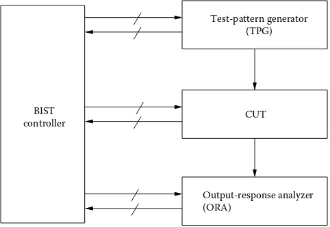
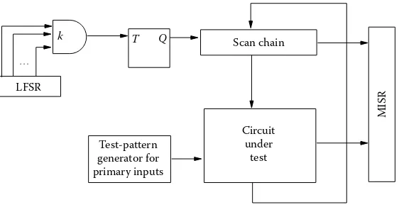
1.4.2 Logic Built-In Self-Test (BIST)
Logic BIST is a DFT technique in which the test-pattern generator and response analyzer become part of the chip itself. Figure 1.2
shows the structure of a typical logic BIST system. In this system,
a test-pattern generator (TPG) automatically generates test
patterns, which are applied to the circuit under test (CUT). The
output-response analyzer (ORA) performs automatic space and
time compaction of responses from the CUT into a signature. The
BIST controller provides the BIST control signals, the scan enable signals, and the clock to coordinate complete BIST sessions for the
Test-pattern generator (TPG)
CUT
Output-response analyzer (ORA)
BIST controller
VLSI Testing ◾ 15
circuit. At the end of BIST session, the signature produced by the ORA is compared with the golden signature (corresponding to the fault-free circuit). If the final space- and time-compacted signature matches the golden signature, the BIST controller indicates a pass
for the circuit; otherwise it marks a fail.
The test-pattern generators (TPGs) for BIST are often constructed from linear feedback shift registers (LFSRs). An n-stage LFSR consists of n, D-type flip-flops, and a selected number of XOR gates. The XOR gates are used to formulate the feedback network. The operation of the LFSR is controlled by a characteristic polynomial f(x) of degree n, given by
f x( )= +1 h x1 +h x2 2+⋯+hn−1xn−1+xn.
Here, each hi is either 1 or 0, identifying the existence or absence of
the ith flip-flop output of the LFSR in the feedback network. If m is the smallest positive integer, such that f(x) divides 1 +xm, m is called
the period of the LFSR. If m= 2n−1, it is known as a
maximum-length LFSR and the corresponding characteristic polynomial is a
primitive polynomial. Starting with a non-zero initial state, an LFSR automatically generates successive patterns guided by its characteristic polynomial. A maximum-length LFSR generates all the non-zero states in a cycle of length 2n−1. Maximum-length LFSRs are commonly used
for pseudo-random testing. In this, the test patterns applied to the CUT are generated randomly. The pseudo-random nature of LFSRs aids in fault-coverage analysis if the LFSR is seeded with some known initial value and run for a fixed number of clock cycles. The major advantage of using this approach is the ease of pattern generation. However, some circuits show random-pattern-resistant (RP-resistant) faults, which are difficult to detect via random testing.
The output-response analyzer (ORA) is often designed as a
m output lines, the number of MISR stages is n, and the number of clock cycles for which the BIST runs is L, then the aliasing probability P(n) of the structure is given by
P n( )=(2(mL n−)−1 2) (/ mL−1), L>n≥m≥2.
If L≫n, then P(n) ≈ 2−n. Making n large decreases the aliasing
probability significantly. In the presence of a fault, the L, m-bit sequence produced at CUT outputs is different from the fault-free response. Thus, if aliasing probability is low, the probability of the faulty signature matching the fault-free golden signature, or the probability of signatures for two or more different faults being the same, is also low.
1.5 POWER DISSIPATION DURING TESTING
Power dissipation in CMOS circuits can be broadly divided into the following components: static, short-circuit, leakage, and dynamic power. The dominant component among all of these is the dynamic power caused by switching of the gate outputs. The dynamic power Pd required to charge and discharge the output
capacitance load of a gate is given by
Pd =0 5. Vdd2 ⋅f C⋅ load⋅NG,
where Vdd is the supply voltage, f is the frequency of operation, Cload is the
load capacitance, and NG is the total number of gate output transitions
(0→1, 1→0). From the test engineer’s point of view, the parameters such as Vdd, f, and Cload cannot be modified because these are fixed for
a particular technology, design strategy, and speed of operation. The parameter that can be controlled is the switching activity. This is often measured as the node transition count (NTC), given by
N T C NG Clo ad All g at e s G
VLSI Testing ◾ 17
However, in a scan environment, computing NTC is difficult. For a chain with m flip-flops, the computation increases m-fold. A simple metric, weighted transition count (WTC), correlates well with power dissipation. While scanning-in a test pattern, a transition gets introduced into the scan chain if two successive bits shifted-in are not equal. For a chain of length m, if a transition occurs in the first cell at the first shift cycle, the transition passes through the remaining (m−1) cycles also, affecting successive cells. In general, if Vi( j) represents the jth bit of vector Vi, the WTC for
the corresponding scan-in operation is given by
WTCscaninVi V ji V ji m j
For the response scan-out operation, shift occurs from the other end of the scan chain. Thus, the corresponding transition count for the scan-out operation is given by
WTCscanout Vi V ji V ji j
1.5.1 Power Concerns During Testing
Due to tight yield and reliability concerns in deep submicron technology, power constraints are set for the functional operation of the circuit. Excessive power dissipation during the test application which is caused by high switching activity may lead to severe problems, which are noted next.
Excessive heat dissipation may lead to permanent damage to the chip.
2. Manufacturing yield loss may occur due to power/ground noise and/or voltage drop. Wafer probing is a must to eliminate defective chips. However, in wafer-level testing, power is provided through probes having higher inductance than the power and ground pins of the circuit package, leading to higher power/ground noise. This noise may cause the circuit to malfunction only during test, eliminating good unpackaged chips that function correctly under normal conditions. This leads to unnecessary yield loss.
Test power often turns out to be much higher than the functional-mode power consumption of digital circuits. The following are the probable sources of high-power consumption during testing:
1. Low-power digital designs use optimization algorithms, which seek to minimize signal or transition probabilities of circuit nodes using spatial dependencies between them. Transition probabilities of primary inputs are assumed to be known. Thus, design-power optimization relies to a great extent on these temporal and spatial localities. In the functional mode of operation, successive input patterns are often correlated to each other. However, correlation between the successive test patterns generated by ATPG algorithms is often very low. This is because a test pattern is generated for a targeted fault, without any concern about the previous pattern in the test sequence. Low correlation between successive patterns will cause higher switching activity and thus higher-power consumption during testing, compared to the functional mode.
VLSI Testing ◾ 19
minimum Hamming distance between state codes. This reduces transitions during normal operation of the circuit. However, when the sequential circuit is converted to scan-circuit by configuring all flip-flops as scan flip-flops, the scan-cell contents become highly uncorrelated. Moreover, in the functional mode of operation, many of the states may be completely unreachable. However, in test mode, via scan-chain, those states may be reached, which may lead to higher-power consumption.
3. At the system-level, all components may not be needed simultaneously. Power-management techniques rely on this principle to shut down the blocks that are not needed at a given time. However, such an assumption is not valid during test application. To minimize test time, concurrent testing of modules are often followed. In the process, high-power consuming modules may be turned on simultaneously. In functional mode, those modules may never be active together.
Test-power minimization techniques target one or more of the following approaches:
1. Test vector are reordered to increase correlation between successive patterns applied to the circuit.
2. Don’t care bits in test patterns are filled up to reduce test power.
3. Logic BIST patterns are filtered to avoid application of patterns that do not augment the fault coverage.
4. Proper scheduling of modules for testing avoids high power consuming modules being active simultaneously.
circuit block depends not only upon the power consumption of the block, but also on the power and temperature profiles of surrounding blocks. Scan transitions affect the power consumption of the blocks, but depending upon the floorplan, heating may be affected.
1.6 EFFECTS OF HIGH TEMPERATURE
With continuous technology scaling, the power density of a chip also increases rapidly. Power density in high-end microprocessors almost doubles every two years. Power dissipated at circuit modules are the major source of heat generation in a chip. Power density of high-performance microcontrollers has already reached 50 W/cm2
at the 100 nm technology node, and it increases further as we scale down the technology. As a result, the average temperature of the die has also been increasing rapidly. The temperature profile of a chip also depends on the relative positions of the power consuming blocks present in the chip. Therefore, physical proximity of high-power consuming blocks in a chip floorplan may result in local thermal hotspots. Furthermore, the three-dimensional (3D) ICs have to deal with the non-uniform thermal resistances (to the heat sink) of the different silicon layers present in the chip. Thus 3D ICs are more prone to the thermal hotspots. High temperature causes the following degradations:
• With an increase in temperature, device mobility decreases. This results in a reduction in transistor speed.
• Threshold voltage of a transistor decreases with an increase in temperature. This results in a reduction in the static noise
margin (SNM) of the circuit.
• Leakage power increases exponentially with an increase in temperature. This may further increase the chip temperature and result in thermal run-away.
VLSI Testing ◾ 21
• Reliability of the chip is also a function of chip temperature. According to the Arrhenius equation, mean time to failure
(MTTF) exponentially decreases with temperature, which is described in Equation 1.1.
MTTF=MTTF0expEa/(kb×T) (1.1)
In Equation 1.1, Ea signifies the activation energy, kb is the
Boltzmann constant. T represents the temperature and
MTTF0 denotes the MTTF at T= 0°K.
Thus, high temperature can severely damage the performance of the chip and may result in component failures.
1.7 THERMAL MODEL
Thermal model plays a crucial role in the efficacy of any thermal management technique. A thermal model used in the context of IC design determines the temperature profile of the chip as a function of its geometric dimensions, packaging, power consumptions of the modules present, and the ambient temperature. The thermal model, discussed here, has been adopted from a popular temperature modeling tool, named HotSpot [2]. This tool works on the principle of the compact thermal model (CTM). Unlike other numerical thermal-analysis methods (for example, the finite
element method (FEM)), CTM takes significantly less run time to
produce a reasonably accurate prediction of chip temperature. A brief description about the working principle of HotSpot has been presented in the following paragraph.
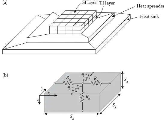
interface layer present below the Si-layer to enhance the thermal coupling between the Si-layer and the heat spreader. Each layer is further divided into several identical (except the peripheral blocks) elementary blocks. The smaller the size of an elementary block, the higher the accuracy and the run time of the thermal model. Power consumption of an elementary block is determined using the power density values of the power-consuming blocks placed in it and their respective areas of overlap with the elementary block. In Figure 1.3a, the Si-layer is divided into sixteen elementary blocks using a 4 × 4 grid mesh. In HotSpot, if the Si-layer contains b number of blocks within it, all the layers below the Si-layer should also be divided into a similar b number of blocks. As shown in Figure 1.3a, along with this 4 ×b number of blocks, the heat spreader layer contains four extra peripheral blocks and the heat sink layer contains eight extra peripheral
SI layer TI layer
Heat spreader
Heat sink (a)
(b)
z y
x
Rx
Sx
Sy Sz
Ry
Ry
Rx
Rz
VLSI Testing ◾ 23
blocks. Therefore, the total number of blocks present in the chip
(Num_Block) is 4× +b 12. A CTM works on the duality between
the thermal and the electrical quantities. Following this duality principle, HotSpot replaces all the elementary blocks in the chip by electrical nodes in their position, containing equivalent resistances and current sources connected to it. Electrical resistance connected to a node is considered to be equivalent to the thermal resistance of that block. The magnitude of the current source connected to a node is set according to the power consumption of the circuit module holding that block. Figure 1.3b shows different horizontal and vertical thermal resistances considered inside a block. Equations 1.2 and 1.3 represent the horizontal thermal resistances, Rx and Ry, along the x- and y-directions, respectively. Equation 1.4 represents the vertical thermal resistance, Rz, along the z-direction. The unit of the
thermal resistance is taken to be K/Watt.
Rx=(1/Klayer)( .0 5×Sx/(Sy×Sz)) (1.2)
Ry=(1/Klayer)( .0 5×Sy/(Sz×Sx)) (1.3)
Rz=(1/Klayer)( .0 5×Sz/(Sx×Sy)) (1.4)
Sx, Sy, and Sz represent the lengths of the block along the x-, y-, and z-directions, respectively. Klayer represents the thermal
it, dimensions and power consumption values of the modules, and the ambient temperature. Using the above information, the conductance matrix [Cond]Num_Block×Num_Block and the power
matrix [Pow]Num_Block × 1 (Num_Block= 4 ×b+ 12) for the
equivalent electrical circuit are calculated. For a particular floorplan, temperatures of the blocks can be calculated by solving Equation 1.5.
[Cond]Num Block_ ×Num Block_ ×[Temp]Num Block_ ×1=[Pow]Num Block_ ××1 (1.5) [Temp]Num_Block×1 represents the temperature matrix, containing
the temperature values for each block in the chip. Equation 1.5 is solved using the LU-decomposition method.
1.8 SUMMARY
This chapter has presented an introduction to the VLSI testing process [3]. The role of testing in ensuring the quality of the manufactured ICs has been enumerated. Different fault models have been illustrated. Design for test techniques have been discussed to enhance the testability of designs. Test-generation algorithms have been enumerated. This has been followed by power and thermal issues in the testing process. Sources of power dissipation, heat generation, and a compact thermal model for estimating chip temperature have been presented.
REFERENCES
1. G. Moore, “Cramming More Components onto Integrated Circuits”, Electronics, vol. 38, No. 8, pp. 114–117, 1965.
2. K. Skadron, M. Stan, W. Huang, S. Velusamy, K. Sankaranarayanan, D. Tarjan, “Temperature-aware Microarchitecture: Extended Discussion and Results,” Univ. of Virginia Dept. of Computer Science Tech. Report CS-2003-08, Tech. Rep., 2003.
25 C H A P T E R
2
Circuit-Level Testing
2.1 INTRODUCTION
A digital VLSI circuit consists of logic elements, such as gates and flip-flops. Test strategies for these circuits consist of applying a set of test patterns, noting their responses, and comparing these responses with the corresponding fault-free values. Depending upon the fault model, a single pattern or a sequence is entrusted with the task of detecting one or more faults. Test patterns are generated by software tools, commonly known as automatic
test-pattern generation (ATPG). The generated test set can often be
found to possess the following properties:
1. A large number of bits in the test set are left uninitialized by the ATPG. Values of these bits are not significant in detecting faults by a particular pattern. These are commonly known as
don’t cares. These don’t-care bits can be utilized in different ways: reducing test-set size via compression, reducing test power and associated heating by circuit transition reduction, and so on.
dedicated pin (called scan-in) is used to input patterns into these flip-flops serially. The contents of these flip-flops are made visible to the outside by shifting them out serially through another dedicated output pin (called scan-out). Introduction of such a scan chain allows the test engineer to consider any sequential circuit as a combinational one and apply combinational ATPG algorithms to generate test patterns for the circuit. However, test-application process becomes longer, as test and response bits are shifted serially through the flip-flop chain. It also creates unnecessary ripples in the chain, which, in turn, cause transitions in the circuit nodes, leading to power consumption and associated heat generation. Test power, as well as thermal optimization, is possible by reordering the test patterns and/or designing the scan chains efficiently.
3. ATPG algorithms often produce more than one pattern per fault. The algorithms may be instructed to stop considering a fault for test-pattern generation (fault dropping) after a fixed number n (say, n= 2, 3, etc.) of patterns have been generated (n-detect test set) targeting that fault. It leaves the scope of choosing the final patterns from the set of redundant patterns generated by the algorithm. The selected pattern set may have good power and thermal implications.
Circuit-Level Testing ◾ 27
get converted to some desired type (rather than D) could be an effective approach toward thermal-aware testing.
The built-in self-test (BIST) approach of testing removes the
requirements for external tester and test-generation algorithms. On-chip pseudo-random sequence generators are used to generate test patterns and apply to the circuit under test. However, BIST generates a large number of patterns that do not detect new faults. Thus, making BIST sessions power- and thermal-aware becomes a challenge.
In the remaining part of the chapter, these temperature-aware testing methods have been discussed in detail. Section 2.2 discusses pattern reordering techniques. Section 2.3 covers a thermal-aware don’t care bit filling strategy. Section 2.4 presents scan-cell optimization. Section 2.5 discusses thermal-aware BIST design, while Section 2.6 summarizes the chapter.
2.2 TEST-VECTOR REORDERING
Vector reordering is an effective tool to reduce circuit transitions during testing. Many of the fault models, particularly those targeting stuck-at faults, are insensitive to the order in which patterns are applied to the circuit. This is especially true for pure combinational and scan-converted sequential circuits. Given a set of test patterns T = {v1, v2, … vn}, vector reordering gives a
2.2.1 Hamming Distance-Based Reordering
This is a highly greedy approach to reduce the peak temperature of circuit blocks. A circuit C is assumed to be consisting of m blocks, {b1, b2, … bm}. Division of C into blocks can be done taking into
view the granularity used for thermal simulation. A coarse grained blocking (involving more circuit elements in a block) will have fewer blocks with faster but less accurate simulation. A finer granularity, on the other hand will require more time for thermal simulation. Let
T= {v1, v2, … vn} be the set of test vectors. The initial ordering Oorig
is considered to be the sequence <v1, v2, … vn>. For this sequence,
power consumed by individual blocks b1, b2, … bm is calculated. A
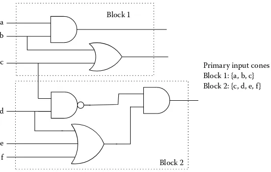
thermal simulation is performed to get the temperature values of all the blocks. The maximum among all of these values is noted. Every block is assigned a weight factor equal to the ratio of its temperature to this maximum. Thus, a weight value close to 1 indicates that the corresponding block is one of those having a temperature close to the peak for the chip. Such a block should get more attention, in order to reduce the peak temperature of the chip, compared with a block having a relatively low weight factor (indicating a relatively cool block). Now, temperature of a block can be controlled by controlling the power consumption in its constituent logic elements. A lesser switching activity in the subset of primary inputs of the circuit that eventually affect the logic gates of the block may have a significant effect on reducing the power consumed by those gates. Keeping this observation in view, the optimization process first identifies the primary inputs of the circuit belonging to the cone of dependency of the blocks. A typical example circuit divided into blocks along with their primary input cones has been shown in Figure 2.1.
Pattern v1 is taken as the first one in the reordered pattern set.
To select the next pattern to follow v1, cost for each remaining
pattern is calculated. Specifically, the activity corresponding to vector vi, Activityi, is calculated as follows. For each block bj, let vij
Circuit-Level Testing ◾ 29
input cone of bj alone. Hamming distance between v1j and vij is
calculated and multiplied by Weightj. Let this product be called Activityij. Thus,
Activityij=Hamming distance v_ ( 1j,vij)×Weightj.
All Activityij values are summed to get Activityi.
Activityi Activityij j
m
=
=
∑
1
In this way, all activities, Activity2, Activity3, … Activityn, are
computed. The minimum among all of these corresponds to the pattern that, if followed by v1, will excite hotter blocks
proportionally less. If this minimum corresponds to pattern vk, it
is removed from the set of patterns Oorig and is taken to follow v1
in the reordered pattern set. Pattern vk now assumes the role of v1,
and the algorithm continues to find the next candidate to follow vk. Block 1
Block 2 a
b
c
d
e
f
Primary input cones Block 1: {a, b, c} Block 2: {c, d, e, f }
The process stops when Oorig becomes empty. The sequence Ofinal
holds the final reordered test set. The whole procedure is presented in the Algorithm Hamming_Reorder.
Algorithm Hamming_Reorder
Input: Set of test vectors {v1, v2, … vn}, Circuit consisting of blocks
{b1, b2, … bm}.
Output: Reordered test vectors in sequence Ofinal.
Begin
Step 1: Set initial order Oorig =<v1, v2, … vn>.
Step 2: Compute block-level power values corresponding to sequence Oorig.
Step 3: Perform thermal simulation to get temperature of blocks
b1 through bm.
Step 4: Set Max_Temp= Temperature of the hottest block among
b1 through bm.
Step 5: For each block bj∈ {b1, b2, … bm}do
Set PI_Conej= Set of primary inputs affecting logic
elements in bj.
Set Weightj = (Temperature of bj) / Max_Temp.
Step 6: Set Ofinal =<v1>; Remove v1 from Oorig.
Step 7: While Oorig≠ϕ do
begin
Let vt be the last vector in Ofinal.
For each vector vk in Oorig do
Activityk=Σmj=1(Hamming distance between parts
of vt and vk affecting block bj) ×Weightj.
Select vector vm with minimum Activitym.
Append vm to Ofinal.
Remove vm from Oorig.
end;
Step 8: Output Ofinal.
Circuit-Level Testing ◾ 31
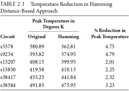
In Table 2.1, the peak temperature values in degrees Kelvin have been reported for a number of benchmark circuits corresponding to test patterns generated by the Synopsys Tetramax ATPG. Temperatures have been reported for the original unordered-test set and the test set obtained via reordering using the Hamming distance minimization approach presented in this section. The percentage reductions have also been noted. It can be observed that the Hamming distance-based reordering approach could reduce the peak temperature in the range of 2% to 4.7%. The scheme is computationally simple as it takes very little CPU time to run the program.
2.2.2 Particle Swarm Optimization-Based Reordering
A major shortcoming of the greedy heuristic approach presented in Section 2.2.1 is that it does not reevaluate the peak temperature behavior of blocks once some of the vectors have changed positions in the ordering. A more elaborate search is expected to reveal more potential orders. In this section, a particle swarm optimization
(PSO) based approach has been presented for the reordering problem which often comes with better solutions.
PSO is a population-based stochastic technique developed by Eberhart and Kennedy in 1995. In a PSO system, multiple candidate solutions coexist and collaborate between themselves. Each solution, called a particle, is a position vector in the search
TABLE 2.1 Temperature Reduction in Hamming Distance-Based Approach
Circuit
Peak Temperature in Degrees K
% Reduction in Peak Temperature Original Hamming
s5378 380.89 362.81 4.75
s9234 393.82 374.95 4.79
s13207 408.15 399.95 2.01
s15850 419.58 410.13 2.25
s38417 453.25 441.84 2.52
space. The position of a particle gets updated through generations according to its own experience as well as the experience of the current best particle. Each particle has a fitness value. The quality of a particle is evaluated by its fitness. In every iteration, the evolution of a particle is guided by two best values—the first one is called the local best (denoted as pbest) and the second one the
global best (denoted as gbest). The local best of a particle is the position vector of the best solution that the particle has achieved so far in the evolution process across the generations, the value being stored along with the particle. On the other hand, the global best of a generation corresponds to the position vector of the particle with the best fitness value in the current generation. After finding these two best particle structures, the velocity and position of a particle are updated according to the following two equations.
vmi +1=wvmi +c r1 1(pbesti−xmi )+c r gbest2 2( m−xmi ) (2.1)
xmi+1=xmi +vmi+1 (2.2)
Here, vmi+1is the velocity of the particle i at the (m+ 1)th iteration,
xmi is the current position (solution) of the particle, r1 and r2 are
two random numbers in the range 0 to 1, and c1 and c2 are two
positive constants. The constant c1 is called the self-confidence
(cognitive) factor, while c2 is the swarm-confidence (social) factor.
The constant w is called the inertia factor. The first term in Equation 2.1 presents the effect of inertia on the particle. The second term in the equation represents particle memory influence, while the third term represents swarm influence. The inertia weight w guides the global and local exploration. A larger inertia weight puts emphasis on global exploration, while a smaller inertia weight tends to entertain local exploration to fine-tune the current search area. The second equation, Equation 2.2, corresponds to the updating of the particle through its new velocity.
Circuit-Level Testing ◾ 33
discrete domain as well. In a discrete PSO (DPSO) formulation, let the position of a particle (in an n dimensional space) at the
kth iteration be pk = <pk,1, pk,2, … pk,n>. For the ith particle,
the quantity is denoted aspki . The new position of particle i is calculated as follows.
pki+1=(w I∗ ⊕c r1 1∗(pk→pbesti)⊕c r2 2∗(pk→gbestk) (2.3)
In Equation 2.3, a→b represents the minimum-length sequence of swapping to be applied on components of a to transform it to b. For example, if a=<1, 3, 4, 2> and b=<2, 1, 3, 4>,
a → b=<swap(1, 4), swap(2, 4), swap(3, 4)>. The operator ⊕
is the fusion operator. Applied on two swap sequences a and b, a⊕b is equal to the sequence in which the sequence of swaps in
a is followed by the sequence of swaps in b. The constants w, c1, c2, r1, and r2 have their usual meanings. The quantity c∗(a→b)
means that the swaps in the sequence a→b will be applied with a probability c. I is the sequence of identity swaps, such as <swap(1, 1),
swap(2, 2), … swap(n, n)>. It corresponds to the inertia of the particle to maintain its current configuration. The final swap corresponding to w I∗ ⊕c r1 1∗(pk→pbesti)⊕c r2 2∗(pk→gbestk) is applied on
particle pki to get particle pki+1. In the following, a DPSO-based
formulation has been presented for the reordering problem.
Particle Structure: If n is the number of test vectors under
consideration, a particle is a permutation of numbers from 1 to n. The particle identifies the sequence in which patterns are applied to the circuit during testing.
Initial Population Generation: To start the PSO evolution
process, the first generation particles need to be created. For the vector ordering problem, the particles can be created randomly. If the population size is x, x different permutations of numbers from 1 to n are generated randomly.
Fitness Function: To estimate the quality of the solution
used. By applying the test patterns in the sequence suggested by the particle, the power consumed by different circuit blocks is obtained. These power values, along with the chip floorplan are fed to a thermal simulator to get the temperature distribution of circuit blocks. However, the approach is costly, particularly for application in evolutionary approaches such as PSO, as the fitness computation must be repeated for all particles in each generation. Instead, in the following, a transition count-based metric is presented that can be utilized to compare the thermal performances of particles.
When a sequence of test patterns is applied to a circuit, each circuit block sees a number of transitions. These transitions lead to proportional consumption of dynamic power by the block. Because power consumption has a direct impact on the thermal behavior of the block, the transition count affects the temperature of the block. However, the temperature of a block is also dependent on the thermal behavior of its neighbors. This needs to be taken into consideration when formulating the fitness function.
First, the transitions in each block corresponding to the initial test-vector sequence are calculated. For block bi, let the quantity
beTinitiali . The block facing the maximum number of transitions
is identified. Let the corresponding transition count be Tmax. To
block bi, a weight factor Wi is assigned, given by Wi= Tinitiali / Tmax.
Thus, Wi is equal to 1 for the block(s) seeing the maximum number
of transitions with the initial sequence of test patterns. Because temperature also depends upon the floorplan, next, the neighbors are identified for each block. A neighbor of a block shares at least a part of its boundary with this block. If {bi1, bi2, … biN} is the set
of neighbors of bi, the average weight of neighboring blocks is
Circuit-Level Testing ◾ 35
Criticality of block bi, CRi, toward thermal optimization is
defined as
CR
W W
i
i avgi
=
+ 1−
1 | | (2.4)
From Equation 2.4, it can be observed that Criticality of a block is a measure of thermal gradient between the block and its neighbors. A higher value of CRi indicates that the neighboring
blocks are also facing transitions similar to the block bi. As a result,
neighbors will possibly have a temperature close to that of bi. The
possibility of heat transfer to the neighbors is less. If CRi is low,
the surrounding blocks of bi are seeing either a higher or lower
number of transitions, on average, compared to bi. Hence, if bi is
experiencing a high numbers of transitions, surrounding blocks are likely to be cooler, enabling the transfer of heat generated at bi
to them, thus reducing the temperature of bi, in turn.
To assign a fitness value to particle p, first the transitions are counted for each circuit block, due to the application of patterns in the sequence specified by p. Let the number of transitions of block
bi corresponding to the pattern sequence p beTpi. The difference
between Tpiand Tinitiali (corresponding to the initial ordering) is
calculated. This difference is multiplied by the weight factor Wi
and criticality CRi of block bi. The sum of these products across all
the blocks of the circuit forms the fitness of p. Thus, the fitness of
p is given by
F itness p Wi CR T T
All blocks i
i pi initiali
( )=
∑
× ×( − ) (2.5)a block is one facing a large number of transitions in the initial ordering, while its surrounding blocks are also having a similar number of transitions.
Evolution of Generations: Once created in the initial population, particles evolve over generations to discover better solutions. As noted in Equation 2.3, at each generation, a particle aligns with the local and global bests with some probabilities. This alignment is effected through swap operations. Consider a particle p= {v1, v2, v3, v4, v5, v6, v7} corresponding to a test pattern set with seven
patterns in it. This particle suggests that the pattern v1 be applied
first, followed by v2, v3, … v7 in sequence. A swap operator swap(x, y) applied on particle p will interchange the patterns at positions x and y in p to generate a new particle. For example,
swap(2, 4) converts p to {v1, v4, v3, v2, v5, v6, v7}. A sequence of
such swap operations are needed to align a particle to its local and global bests. For example, to align a particle p= {v1, v4, v3, v5, v2, v7, v6} with its corresponding local best, say {v2, v4, v5, v7, v1, v6, v3}, the swap sequence is {swap(1, 5), swap(3, 4), swap(4, 6), swap(6, 7)}. Once the swap sequences to align a particle with its local and global bests have been identified, individual swaps are applied with some probabilities. For the local best, it is c1r1, and for
the global best, it is c2r2.
Particles evolve over generations through the sequence of swap operators. To determine the termination of the evolution process, two terminating conditions can be utilized as noted next.
1. PSO has already evolved for a predefined maximum number of generations.
2. The best fitness value of particles has not improved further for a predefined number of generations.
Circuit-Level Testing ◾ 37
Algorithm DPSO_Reorder
Input: A set of n test vectors with an initial ordering. Output: Reordered test-vector set.
Begin
Step 1: For i= 1 to population_size do // Create initial population. begin
particle[i] = A random permutation of numbers
1 to n;
Evaluate Fitness[i] using Equation 2.5;
pbest[i] =particle[i]; end;
Step 2: gbest= particle with best fitness value;
generations= 1;
gen_wo_improv= 0;
Step 3: While generations <MAX_GEN and gen_wo_improv
<MAX_GEN_WO_IMPROV do
begin // Evolution through generations
old_gbest= gbest;
For i= 1 to population_size do begin
Swap_seqlocal= Swap sequence to align
particle[i] with pbest[i];
Swap_seqglobal= Swap sequence to align
particle[i] with gbest;
Generate two random numbers r1 and r2 in
the range (0,1);
particle[i] = Resulting particle via application
of Swap_seqlocal and Swap_seqglobal to particle[i]
with probabilities c1r1 and c2r2;
Evaluate Fitness[i] using Equation 2.5; If Fitness[i] < fitness of pbest[i], set pbest[i]
= particle[i];
If Fitness[i] < fitness of gbest, set gbest
end;
If (gbest = old_gbest) then gen_wo_improv++;
generations++;
end;
Step 4: Output gbest; End.
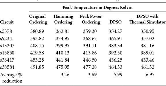
Table 2.2 reports the peak temperature values in degrees Kelvin under different ordering policies for a number of benchmark circuits. The first column notes the name of the circuit. The second column reports the peak temperature values with the input ordering of test vectors. The column “Hamming ordering” corresponds to the Hamming distance-based reordering policy suggested in Section 2.2.1. The column marked “Peak power ordering” corresponds to a DPSO implementation of the reordering policy in which, as the fitness measure, only the peak power consumed by circuit blocks have been considered. The optimization algorithm thus attempts to minimize this peak power consumption. The resulting peak temperature values have been reported in the table. The column marked “DPSO” contains results corresponding to the DPSO formulation presented in this section. The last column is another modified version of the DPSO algorithm. Here, instead of modeling the fitness of a particle
TABLE 2.2 Temperature Reduction in DPSO-Based Approach
Circuit
Peak Temperature in Degrees Kelvin Original
s5378 380.89 362.81 359.30 354.27 350.95
s9234 393.82 374.95 368.67 365.91 357.02
s13207 408.15 399.95 391.11 383.34 381.16
s15850 419.58 410.13 413.86 392.50 389.01
s38417 453.25 441.84 446.50 436.25 433.46
s38584 491.85 475.95 477.28 464.33 461.32
Average % reduction