GAS SENSING PROPERTIES OF RUTILE-TiO2 (100) FILMS PREPARED BY PULSED
LASER DEPOSITION
Bambang Siswanto*, Shunya Yamamoto** and Masahito Yoshikawa**
* Center of Accelerator and Material Process Technology-Batan of Indonesia, Po. Box. 6101 ykbb, Yogyakarta 55281
**Department of Materials Development, JAERI Takasaki, 1233 Watanuki, Takasaki, Gunma 370-1292, Japan
ABSTRACT
GAS SENSING PROPERTIES OF RUTILE-TiO2 (100) FILMS PREPARED BY PULSED LASER DEPOSITION. The
gas sensing property of TiO2 thin films have been demonstrated in rutile-TiO2 (100) films grown on the α-Al2O3 (0001) substrates by Pulsed Laser Deposition (PLD). High quality rutile-TiO2 (100) films were successfully grown on α-Al2O3 (0001) with the substrate temperature at 500oC under 15 mTorr of O2 gas pressure. The thickness and crystallinity of TiO2 films were evaluated by Rutherford backscattering spectrometry combined with channeling (RBS/C) and X-ray diffraction using θ-2θ scans. To evaluate CO2 gas sensing property of TiO2 films, the dependence of the changing of electrical resistivity on the temperature was measured. It’s found that high crystallinity rutile-TiO2 (100) films on the α -Al2O3 (0001) substrate kept at 100oC exhibits good gas sensing property for CO2 gas.
Keywords: X-ray diffraction, laser epitaxial, TiO2 thin film, electrical resistivity, CO2
INTRODUCTION
itanium dioxide (TiO2) has been considerable interest from viewpoint of basic science and applications. For example the TiO2 is used in heterogeneous catalysis, as photo-catalyst, in solar cell for the production of hydrogen and electric energy, as corrosion-protective coating, as an optical coating in ceramic, in electric devices such as varistors, and as gas sensor. More researchers have been interest a great was addressed in the
characterization of the structural and electrical properties of thin film for gas sensing(1). The TiO2 is extensively
used as gas sensors due to their properties, which changes their electrical resistivity under gas exposures(2-4). TiO2
is also interesting candidate for conductance-type gas sensor devices for the detection of NO2 (5), ethanol(6), and
CO2 (7). Usually, the resistivity of TiO2 is high in low temperature, and that decreased at high temperature as the
examples shown in references(8,9). Fully oxidized the TiO2 is an insulator with a resistivity on the order of 1013
ohm-cm. As the remove oxygen atoms from the TiO2 lattice, the electrical resistivity decreases and begins to act like
n-type semiconductor [10]. It is generally believed that, a gas sensor should have a high selectivity and sensitivity to
the target molecule. Also a short response time and stability are requested. Sensitivity and response time to gas are strongly influenced by the quality of the thin films, such as crystal structure, microstructures, chemical composition and the ohmic contact. TiO2 films have been prepared by several deposition techniques such as
conventional sputtering[11],and RF helicon magnetron sputtering [12]. In this present study, the rutile-TiO2 films were
prepared by pulse laser deposition (PLD) under controlled oxygen low-pressure. The crystal quality, the crystallographic orientation relationships between film and substrate with using XRD and RBS/channeling and the electrical properties including the sensitivity and response to CO2 are reported.
T
METHOD
The epitaxial-TiO2 films were deposited on the α-Al2O3 substrates by pulse laser deposition (KrF-Eximer
laser, wavelength: 248 nm, Lambda Physik). The α-Al2O3 substrates were obtained commercially (mirror-polish at
both sides) and the typical size is 10 × 10 × 0.3 mm3. The substrates were cleaned ultrasonically in acetone at 15
min and also in water at 5 min. The PLD chamber was pumped down to 6×10⁻⁵ Pa using a turbo molecular pump
(TMP). The laser beam incident was focused to the evaporation target with incident angle of 45o. Typical laser
energy and repetition rate were 150 mJ/cm2 and 5 Hz. The evaporation target to substrate distance was about 50
mm. Both the target stage and the substrate holder were rotate during deposition. The single crystal rutile-TiO2
(φ30 mm) was used for the evaporation target. To oxidize and form TiO2 film, oxygen gas (purity 99.99%) was
under the pumping condition. In this study, TiO2 films with 300∼500 nm in thickness were deposited at 500oC under an oxygen pressure at 2 Pa. The crystallographic relationship between TiO2 films was determined by X-ray diffraction measurement using a high-resolution diffractometer (X’Pert-MRD, Phillip). The X-ray source was
operated at 40 kV and 30 mA for Cu-Kα radiations. Rutherford backscattering/channeling (RBS/C) analysis using 3
MV single-stage of accelerator at JAERI/Takasaki was employed to characterize the epitaxial-TiO2 films. The
analyzing 2.0 MeV 4He+ ions were incident into the sample and backscattered particles were detected at 165o
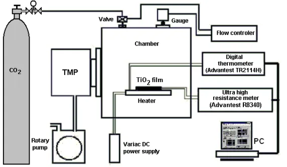
scattering angle with a surface barrier detector. The beam size was 1 mm in diameter and the beam current was 15 nA typically. Samples were mounted on a three-axis goniometric to pattern the planar channeling and the axial channeling in angular coordinate. The thickness and the crystallinity of TiO2 films were evaluated from RBS/C spectra. The electrical resistivity of deposited films under the CO2 gas atmosphere was measured by using the measuring equipment illustrated in Figure 1. The two-probe method was used with Au-contacts sputtered on the
TiO2 films. The chamber was pumped down to 6 × 10⁻⁵ Pa by a TMP, and then the CO2 gas was flowed into the
chamber through a mass-flow meter controlled by an absolute pressure gauge (Baratron 250, MKS) under the pumping condition The deposited TiO2 films were heated by the ceramic heater and temperatures were monitored by a thermocouple placed next to sample.
Figure 1. The instrument system measured of electrical properties including the sensitivity to CO2.
RESULTS AND DISCUSSION
The crystal structure of deposited TiO2 thin films was examined with X-ray diffraction technique. Figure 2
shows a typical θ-2θ X-ray diffraction pattern from the TiO2 film on the α-Al2O3 (0001) substrate. The film was
deposited at 500oC with about 507 nm thickness. In this case, only the reflections from the rutile-TiO2 (200) and
(400) are observed without any reflections from the α-Al2O3 substrate, which indicates that the only rutile-TiO2
(100) films are epitaxially grown on the (0001) plane of α-Al2O3 substrate. The peak positions at 2θ = 39.97o and
85.89o correspond to the reflection from rutile-TiO2 (200) and (400), respectively
.
As the result, high quality rutiletype TiO2 (100) film were successfully obtained on α-Al2O3 (0001) with the substrates temperature kept at 500oC
and an exhaled to 2 Pa of O2 gas pressure.
RBS/channeling was employed to characterize TiO2 films grown on α-Al2O3 (0001) substrates. Figure 3
shows the 2.0 MeV4He+ RBS spectra from the rutile-TiO2 (100) film on the α-Al2O3 (0001) taken under random and
the TiO2<100> aligned condition. The thickness of the film estimated by RBS spectra is 507 nm. From these RBS
spectra, one can recognize clearly the separated peaks from TiO2 film and α-Al2O3 substrate. The peaks at 1.43
and 0.88 MeV correspond to Ti component in the TiO2 film and Al component in the α-Al2O3 substrate. Judging by
the peaks intensity, the high quality TiO2 film is grown up from the interface and the interface is not mixed with
each other within the depth resolution (∼10 nm) of this technique. The minimum yield, χmin value, the ratio between
degree of disorder in crystalline solids. The χmin value in the <100> aligned spectrum is 0.039 at the just area behind the surface peaks of the TiO2 film, which suggests that the crystal quality of the film is high enough as that in bulk single-crystal even if includes twins. In the peak from Ti component under the aligned spectra, one can recognize two peaks at both sides of the TiO2 film. The peak at the high-energy side corresponds to the surface
peak and the peak at the low-energy can be attributed to the imperfections at the boundary layer adjacent to the α
-Al2O3 (0001) substrate. The planar channeling analysis around the mayor axes of the TiO2 film and the α-Al2O3
gives the evidence that the TiO2 (100) crystallographic axis is parallel to the α-Al2O3 (0001) axis.
Figure 2. X-ray diffraction patterns from the epitaxial rutile-TiO2 films on the α-Al2O3 (0001) substrate. The films
were deposited at 500oC under the O2 gas pressure of 15×10-3 Torr.
Figure 3. The 2 MeV 4He+ RBS/channeling spectra from a rutile-TiO2 film with the thickness approximately 507
nm on the α-Al2O3 (0001) substrate. The aligned spectrum was taken with the beam directed along the
(100) axis of the rutile-TiO2 film. The film was deposited at 500oC under the O2 gas pressure of 15×10-3
Torr.
The electrical resistivity of deposited films was measured as a function of temperature (30-200 oC). In figure
4 shows the resistivity of the rutile-TiO2 (100) film annealed at 300oC/4h in air as function of temperature. The
measurement was carried out at the pressure about 6×10⁻⁵ Pa. The heating of film at 200oC, the resistivity
to the temperature at 30 oC. The resistivity of deposited film is exponentially dependant on the temperature which indicated the TiO2 films have n-type semiconductor behavior. Similar behavior has been observed for the resistivity
of as-deposited films. But the resistivity of the film was increased after cooling down to the temperature at 30oC. It
has been assumed that the as-deposited films are not enough to oxidize in the vacuum conditions. We find the
values of resistivity to be quite similar to those of the films after annealing at 300 oC in air. The TiO2 film with
doping metal showed fairly good sensing characteristics to NO2 at 600oC(5). The resistivity of TiO2 bulk at 1200oC is
in order 8.5 Ωcm(8). The thin film TiO2 was found to crystallize to a dense columnar layer of nano-crystalline
rutile-TiO2 upon annealing at 400oC, their conductivity was quite sensitive to changes in the ambient oxygen pressure
between 200 and 325oC[13]. Nevertheless, in this work, the resistivity of rutile-TiO2 thin film less than 10 Ωcm was
obtained by the annealing 300oC/4h and if its films have been annealed at higher than 400oC, the resistivity of film
increased on the order kΩcm. For practical use, high resistivity of TiO2 films is not suitable for the gas sensing
material since the resistivity measurement is needed an ultra high resistant meter.
Figure 4. The resistivity of the rutile-TiO2 (100) film annealed at 300oC/4h in air as function of temperature. The
measurement was taken at the chamber condition under pressure of 6×10⁻⁵ Pa.
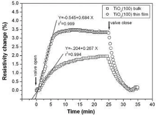
Figure 5. Curve response of rutile-TiO2 (100) bulk and thin film to CO2. The heating was set at 100oC and the
In the following, we compare the gas sensing properties, i.e. time-dependent changes of the electrical resistivity of the single-crystal rutile-TiO2 (100) bulk and the as-deposited film upon exposure to 5 mTorr of CO2 gas
pressure. It is shown in Figure 5. The sample is kept at temperature of 100oC. Before the exposing CO2 gas, the
resistivity of the rutile-TiO2 (100) and the deposited film is 2.76 Ωcm and 2.27 Ωcm, respectively. When the
samples were exposing CO2, the resistivity of TiO2 (100) bulk and thin film were increased. The increasing resistivity upon CO2 exposure is explained the participation of free charge carriers, i.e. electrons, in TiO2 during
CO2 absorption[10]. From both the curves in Fig 5, the maximum value of resistivity change exposing CO2 gas was
obtained at 1.75% and 3.5% for the TiO2 bulk and thin film, respectively. In comparison between the TiO2 bulk and the film, the resistivity change of TiO2 bulk was lower than that of the film. This matter, the TiO2 films have more sensitive to CO2 than that of bulk sample. Possibility, the TiO2 films are reasonable for CO2 gas sensing material. Here, one can see that both the resistivity of TiO2 (100) bulk and thin film increased linearly when the times about 5
min to exposure of CO2. The better linearity correlation coefficient (r2= 0.994 and r2= 0.999) was obtained using
TiO2 (100) bulk and thin film sample in time intervals at 0 - 5 min. The tangent direction of linear regression the TiO2 (100) bulk is lower than that of the thin film, which indicates that the TiO2 (100) films have short response time in compression with the bulk sample. In additional, the resistivity of TiO2 bulk and thin film were decreased towards to initial values, which recognizes that TiO2 film is suitable for gas sensor material.
CONCLUSION
The successful growth of the rutile-TiO2 thin films by pulse laser deposition was demonstrated in detail. The
high quality of rutile-TiO2 (100) film was grown on the α-Al2O3 (0001) substrate with a thickness 507 nm. The high
quality of film was characterized using XRD and RBS/Channeling. The electrical properties including the sensitivity and response time to CO2 were demonstrated. The resistivity of TiO2 (100) films have been obtained in order a
value 1 – 6.4 Ωcm at an interval of measurement to 30 – 200oC. The TiO2 (100) film with subsequent annealing to
300oC/4h significantly enhanced the sensitivity to CO2. Also, that having the best overall characteristics of good
response and recovery time (both <5 min), better linearly correlation (r2= 0.999) at the interval time 0 − 5 min,
100oC and an exhaled to 5 mTorr of CO2 pressure. Therefore, the high quality of rutile-TiO2 (100) film prepared by
pulsed laser deposition under low-controlled oxygen pressure is suitable for CO2 gas sensor material.
REFERENCES
1. H. TANG, K. PRASAD, R. SANJINES, P. E. SCHMID, AND F. LEVY, J. Appl. Phys. 75(4), (1994) 2042-2047
2. F. BOCCUZZI, E. GUGLIELMINOTTI AND A. CHIORINO, Sensor and Actuators B7 (1992) 645-650
3. A. ROTHSCHILD, F. EDELMAN, Y. KOMEM, AND F. COSANDEY, Sensor and Actuators B67 (2000)
282-289
4. P. –G. SU, WU REN-JANG, NIEH FANG-PEI, Talanta 59 (2003) 667
5. YASUSHI YAMADA, YOSHIKI SENO, YUMI MASUOKA, TADASHI NAKAMURA AND KATSUJI
YAMASHITA, Sensor and Actuators B66 (2000) 164-166
6. A. RUIZ, G. DEZANNEAU, J. ARBIOL, A. CORNET, J. R. MORANTE, Thin Solid Films 436 (2003) 90-94
7. P. PARSIEB, S. KOMORNICKI, R. GAJERSKI, S. KONZINKI, M REKAS, Solid State Ionics, 157 (2003)
357-363
8. U. DIEBOLD, Surface Science Report 48(2003) 53-229
9. A.L. LINSEBIGLER, G. LU, J.T. YATES JR., Chem. Rev. 95(1995) 735
10. JOHN R. MCCORMICK, JOHN R. KITCHIN, MARK A. BARTEAU, JINGGUANG G. CHEN, Surface Science 545 (2003) L741-L746
11. LEI MIAO, SAKAE TANEMURA, PING JIN, KENJI KANEKO, ASUKA TERAI, NATALIYA NABATOVA-GABAIN, Journal of Crystal Growth 254 (2003) 100-106
12. A. VOIMERO, G. DELLA MEA, M. FERRONI, G. MARTINELLI, G. RONCARATI, V. GUIDI, E. COMINI, G. SBERVEGLIERI, Materials Science and Engineering B101(2003) 216-221