property tuning via thickness and stacking
Juan Xia, Jiaxu Yan
⇑, Ze Xiang Shen
⇑Division of Physics and Applied Physics, School of Physical and Mathematical Sciences, Nanyang Technological University, Singapore 637371, Singapore
a r t i c l e
i n f o
Article history: Received 2 June 2017 Revised 9 June 2017 Accepted 9 June 2017 Available online 19 June 2017
Keywords:
Transition metal dichalcogenides Interlayer coupling
Raman spectroscopy Photoluminescence Spin-valley polarization Second harmonic generation Electronic performance
a b s t r a c t
Two-dimensional (2D) transition metal dichalcogenides (TMDs) have attracted intense interests owing to their fascinating physical properties and potential applications. In addition, the properties of few-layer TMD materials can be tuned by their thickness as well as the stacking sequence. For instance, MoS2/WS2/MoSe2/WSe2undergoes a transition from the indirect-band-gap to direct-band-gap
semicon-ductors with their thickness reduced to monolayer; the weak van der Waals (vdWs) interaction between the layers in TMDs endows various stacking sequences that can be facilely obtained by different methods. Hence, thickness and stacking sequence can be used to modulate the electronic band structures, valley polarization and nonlinear optical properties, providing additional useful and convenient ways to manip-ulate the materials and fabricate devices with novel functionalities. Here we review recent progress in thickness and stacking engineering for TMD materials in structural, optical and electronic properties. Last, we offer our perspectives and challenges in this research field.
Ó2017 Published by Elsevier B.V.
Contents
Introduction. . . 1
Growth and stacking characterization of layered TMDs . . . 2
Thickness- and stacking-dependent interlayer coupling . . . 4
Spin-valley polarization in few-layer TMDs . . . 9
Second harmonic generation (SHG) in stacked-TMDs. . . 13
Thickness and phase engineered TMD electronic devices . . . 16
Conclusion . . . 17
Acknowledgements . . . 17
References . . . 18
Introduction
Layered transition metal dichalcogenides (TMDs) have attracted intense attention among the two-dimensional (2D) materials, which stem from their intriguing physical properties that have great potential for many applications, such as optical, electronic and optoelectronic devices[1–3]. Moreover, these physical proper-ties of layered TMDs are strongly correlated to thickness[4], strain [5], pressure[6], stacking sequence[7]and electromagnetic field
[8]. For instance, it is already known that MoS2/WS2/MoSe2/WSe2 undergoes a transition from the inband-gap to direct-band-gap transition when the thickness is reduced to monolayer [1,4]. This thickness-dependent bandgap in TMDs can be explored to the next-generation electronic and optoelectronic devices. Beyond this, the weak van der Waals (vdWs) force between the layers allows TMD materials to be grown with different stacking sequences that governs the crystal symmetry and in turn signifi-cantly influence the electronic band structures, magnetism, super-conductivity, valley polarization, nonlinear optical effects, and other physical properties[9–11]. Hence stacking provides another convenient method to manipulate TMDs functionalities.
http://dx.doi.org/10.1016/j.flatc.2017.06.007
2452-2627/Ó2017 Published by Elsevier B.V.
⇑ Corresponding authors.
Our group has reported detailed experimental study and theo-retical simulation of Raman vibrations and band structures for AA/AB bilayer (2L) and AAB/ABB/ABA/AAA trilayer (3L) MoS2 sam-ples by chemical vapor deposition (CVD) method, which exhibit different coupling phenomena in both photoluminescence (PL) and Raman spectra [12]. The ultra-low-frequency (ULF) Raman vibrational bands are particularly sensitive to the interlayer inter-action and hence the stacking sequence between layers. We demonstrate that the evolution of interlayer interaction with various stacking configurations correlates strongly with the layer-breathing mode (BM) and interlayer shear mode (SM). Ab
initiocalculations reveal that the thickness-dependent properties
arise from both the spin-orbit-coupling (SOC) and interlayer cou-pling in different structural symmetries[13]. A bond polarizability model is used byLuoet al.[14]to show the Raman intensity of SM is sensitive to the stacking configurations and these stacking-dependent ULF Raman features in layered TMDs provide a practical and efficient method to identify the stacking configurations.
Another intriguing character related to spin-valley polarization in TMDs is also mediated by stacking configurations[15–17]. Speci-fic to 1L MoS2(WS2), the SOC splits the valence bands by 160 meV (500 meV) with opposite spin signs near the K/K’ valley. Together with the time-reversal symmetry, the spin and valley are inherently coupled, leading to valley-contrasting optical dichroism. Conse-quently, one can selectively excite the carriers using circularly polarized light, i.e. left (right) circularly polarized light for excita-tion of spin up (down) electrons at K (K’) valley, making monolayer MoS2the ideal material for valleytroincs[18]. Bilayer TMDs offers another degree of freedom named as layer pseudospin [19–24], which refers to the carriers’ location, either upper, middle or lower layer and so on. The interplay among spin, valley pseudospins and layer pseudospins opens an unprecedented platform for the control of quantum states, where both spin and valley possess magnetic moments and can be manipulated by magnetic and optical means [25–28], while the layer pseudospin can be tuned by an electric field [24]. Numerous have been published in the literature to exploit these quantum controls in monolayer and bilayer TMDs. In even-layer TMD samples, the presence of inversion symmetry and time-reversal symmetry ensures that the electronic states are doubly spin-degenerate. However, the inversion symmetry is bro-ken in odd-layer TMDs, resulting in the splitting of valence bands due to the presence of SOC. Along with the layer number, stacking configuration also has a significant influence on the properties [9,11,29]. For instance, 2H bilayer MoS2 is inversion symmetric without SOC, and hence the valley-contrasting optical selection rule becomes invalid [16]. Recently, pioneering experiments have demonstrated that valley-dependent spin polarization can be real-ized in non-centrosymmetric phases including 3R phase, folded bilayer[19,30], and bilayer systems under perpendicular electric fields[20,21]. Such manipulation of intrinsic symmetry and spin in even-layer or bulk TMDs has greatly enriched the scope of valley physics and plays a crucial role towards spintronics and valleytron-ics[31,32].
Besides the structural, electronic, and linear optical properties of TMDs, their nonlinear optical properties, especially second har-monic generations (SHG) have been studied, where the lack of inversion symmetry in monolayer TMDs leads to a strong optical SH response. Bulk 2H-MoS2 crystal belongs to space group D6h, which possesses inversion symmetry different from monolayer. Consequently, the second-order nonlinear response for 2H-MoS2 bulk should vanish [32]. It has been reported that the second-order nonlinear susceptibility for MoS2bulk is around 10 14m/V, much smaller than that of monolayer (10 7m/V). This SHG effect proves to be highly sensitive to the thickness, crystalline orientation, as well as stacking configuration [33,34]. So far, thickness-dependent optical SHG in odd-layer TMDs have been
found [35–38], attributed to the non-trivial second-order nonlinearity due to the broken inversion symmetry.Hsuet al. have studied the SHG of artificially stacked bilayer MoS2 with various twist angles. The SHG signals can be described as the coherent superposition of SH signal from individual layer involving a phase difference relying on the twist angle. Therefore, the stacking-dependent polarization of SHG intensity can be served as one accu-rate and powerful characterization tool to identify their atomic stacking orders[39].
The nature of TMDs, such as appropriate bandgap, high carrier mobility, high current on/off ratios, and thickness-dependent band structure makes TMDs as promising materials for various devices [40,41], such as field-effect transistors (FETs), photovoltaics, pho-todetectors, and nonvolatile memories[42–46]. From literature, most electronic devices are constructed using thep-n junctions through heavy doping, Schottky junctions between metal and semiconductor, vdWs heterojunctions by mechanical transfer and thickness-/strain-induced homojunctions. For example, the diode-like rectification effect and remarkable drain-source current have been demonstrated in TMDs-based materials, such as
thickness-dependent MoX2 homojunctions [47–49],
phase-modified 1T’-2H MoX2 Schottky junctions [50], WS2-WSe2 [51], WX2-MoX2[52–56]heterojunctions. Inref[47], He et al. reported that a series of thickness -dependent 3R-MoSe2junctions exhibit current rectification and photovoltaic behaviors, and yet without heavily doping strategies in TMDs[50] or TMDs heterojunction fabrication [17]. The first-principles calculations show that the thickness -dependent band alignment determines the electronic and optoelectronic behaviors in such junctions. Moreover, layer-engineered homojunctions can be prepared through one-step CVD growth approach that is much simpler than the preparation processes for TMD heterojunctions. Such strategy provides guid-ance for designing and fabricating possible layer-engineered devices. Similarly, the layer-engineered homojunctions with 2H stacking and the stacking-dependent (e.g. 2H-3R bilayer) TMD homojunctions are expected to exhibit novel electronic and opto-electronic properties.
Growth and stacking characterization of layered TMDs
and MoS2prepared by different methods[61]. The red and blue curves show the mobility of graphene and MoS2samples on SiO2. On one hand, both graphene and MoS2samples from the mechan-ically cleaved method show the best structural and electronic qual-ity, due to fewer defects. On the other hand, CVD/PVD grown samples provide more stacking variations to investigate interlayer coupling effect on optical, electronic, electrical and other intriguing physical properties.
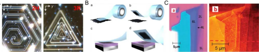
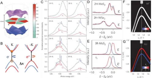
From the first-principles calculations, there are five high-symmetry stacking configurations for bilayer MoS2as shown in Fig. 3A, which can be classified into two groups depending on whether the S (Mo) atoms in the top layer are directly situated above the Mo (S) atoms of the bottom layer. The optical image (Fig. 3A centre) shows that PVD grown bilayer MoS2sheets exhibit two typical configurations: two triangles in the same orientation
(marked as AA) and in reverse orientation (marked as AB). Our previous results indicate that AA and AB stackings are the most favorable among all configurations while other three are energeti-cally unstable. The two natural polytypes of MoS2are known as 2H (space group:P63/mmc) and 3R (space group:R3m) respectively, both of which have trigonal prismatic coordination of the Mo atoms but with distinct stacking orders[11,12].Fig. 3B shows the optical and Z-contrast scanning transmission electron microscopy (STEM) images of the 1L (left), AA- (middle) and AB- (right) stacked 2L MoS2. The STEM images clearly show the distinct arrangements between AA and AB stacked bilayer samples. In STEM, the intensity sensitively relies on the atomic weight and the number of layer, where the high intensity sites correspond to the heavy atoms (Mo) and thicker samples, leading a contrast difference. In the 3L MoS2samples, there are four typical stacking patterns: ABA, AAA, Chemical Society.
Fig. 2.Vapor deposition of few-layer MoS2samples. The temperature ramping diagram of the growth process and morphologies of as grown MoS2flakes by PVD (A) and CVD (B) respectively. (C) Mobility comparison of graphene and MoS2grown by various methods. The red curve shows the mobility of graphene on SiO2, and the blue curve is for MoS2on SiO2. The mechanically cleaved samples show the best structural and electronic quality for both graphene and MoS2. Reproduced with permission from Ref.[59]. Copyright 2014, Nature Publishing Group.
AAB and ABB following the nomenclature of bilayer system, which lead to three distinct stacking configurations as the ABB and AAB configurations are completely equivalent. The top and side views of atomic structures for ABA-, AAA- and AAB-stacked 3L MoS2are shown inFig. 3C, where the layer number is determined by both optical images and Raman intensity mapping[12,31].
Thickness- and stacking-dependent interlayer coupling
The electronic properties of 2D materials are affected by both layer number and stacking configurations through interlayer cou-pling [62–64]. The different Raman behaviors for both high-frequency and low-high-frequency modes as a function of layer number have been revealed and widely discussed in recently years. Raman spectroscopy is a greatly potent and efficient approach to investi-gate the thickness variation and phase transition behaviors in 2D materials, especially the ultra-low-frequency (ULF) Raman spec-troscopy, which is highly sensitive to interlayer interactions and can reflect even the minute changes and discrepancies of structure. Affected by layer numbers and layer stacking, both shear modes (SMs) and layer breathing modes (BMs) have been observed that exhibit strikingly different features for different configurations, which can be well modeled using linear chain simulations[12]. Thus, polarized ULF Raman technique can be used as a fast and convenient nondestructive method to identify stacking sequence, which is otherwise very difficult using other techniques.
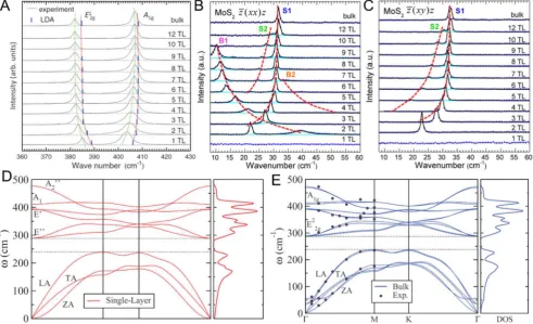
The Raman frequency trends in MoS2crystal from 1L to 12L are studied both theoretically and experimentally in Fig. 4. The Raman-active in-plane E1
2gmode stiffens whereas the out-of-plane
A1g mode softens with decreasing thickness. The black curves are the experimental results and the density functional theory (DFT) cal-culations are plotted in blue bars, showing the consistent frequency evolution trends (Fig. 4A). The red shift of the A1g mode with decreasing layer number is attributed to the smaller restoring force, while there are several explanations to the blue shift of E1
2gmode, which has been ascribed to thickness-induced structure modifica-tion, long-range coulomb interactions, or enhanced surface force constant of Mo-S intralayer interactions in few-layer MoS2[65]. Sim-ilar thickness-dependent phonon evolutions can be also found in low-frequency SMs and BMs, as shown inFig. 4B and C, where two optical configurations (z(xx)z (4B) and z(xy)z (4C)) are utilised. Based on the Raman tensor, the interlayer SMs and E1
2g mode are shown in bothz(xx)z andz(xy)z configurations, whereas the inter-layer BMs and A1gmode are observed only in thez(xx)z configura-tion. InFig. 4B and C[66], from bulk to 2L, the S1 peak red shifts from32 cm 1 to
22 cm 1. In contrast, the other predominant peak B1 blue shifts and crosses the S1 peak at 3L. As discussed before, the frequency evolutions of E1
2gand A1ghave been used to determine the layer number of TMD samples[29]. However, these two peaks are much less sensitive to the thickness than the inter-layer SM and BM peaks. Two weak peaks, labelled S2 and B2, exhibit the similar trends versus thickness with S1 and B1.Fig. 4D and E show the phonon dispersions and density of states (DOS) for 1L (4D) and bulk MoS2(4E) with experimental data plotted in black dots[67]. Different from monolayer MoS2, the bulk phonon disper-sion has three acoustic modes, the in-plane longitudinal acoustic (LA) mode, transverse acoustic (TA) mode and out-of-plane acoustic (ZA) mode, whereas, the low-frequency optical modes are found at 35.2 and 57.7 cm 1, corresponding to the rigid-layer lateral and
ver-Fig. 4.Thickness-dependent Raman behaviors of MoS2. (A) Experimental and LDA-calculated high-frequency Raman for few-layer and bulk MoS2. Reproduced with permission from Ref.[63]. Copyright 2013 American Physical Society. The E1
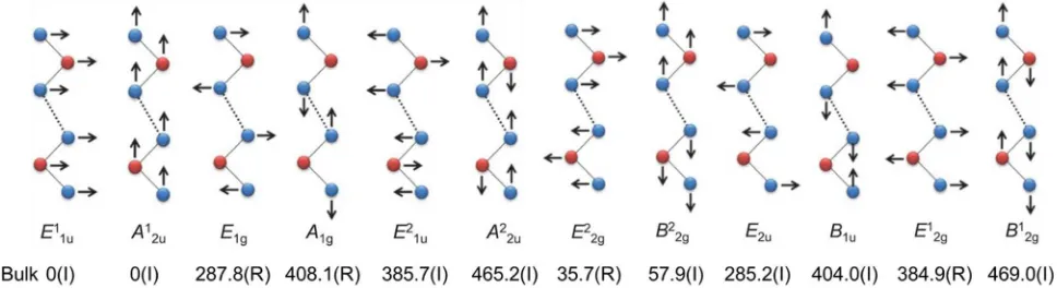
tical motion, respectively. Based on group theory[50], the phonon modes at C-point for bulk MoS2 can be decomposed into the irreducible representation: C= 2A2u+ 2E1u+ 2B2g+ 2E2g+ A1g+ E1g+ B1u+ E2u. These 12 irreducible representations in bulk MoS2 can be divided into six conjugate pairs (E1
1uand E22g, E1gand E2u, E2
1u and E12g, A12uand B22g, A1g and B1u, A22uand B12g), as shown in Fig. 5. In each conjugate pair, there is an inversion centre between the two layers, and one phonon mode differs from the other by an interlayer phase shift of 180°.Fig. 5shows all the displacement rep-resentations for theC-point vibrational modes in bulk MoS2with frequencies shown below, where R and I represent Raman active and inactive vibrations respectively. All these calculated phonon fre-quencies are consistent with previous experimental results[65].
It has been reported that MoS2/WS2/MoSe2/WSe2undergoes a transition from the indirect-band-gap to direct-band-gap semicon-ductor with their thickness reduced to monolayer. Correspond-ingly, the PL quantum yield (QY) shows an obvious enhancement while the TMD crystal undergoing from the indirect-gap bulk to the direct-gap monolayer[68]. Systematic studies of the evolution of the optical properties and electronic structures in layered TMD crystals as a function of layer number (N) have been reported. With the reduction of thickness, the confinement-induced band gap var-ies from the bulk value of 1.29 eV to over 1.90 eV in monolayer. Moreover, the change in the energy of indirect band gap atCpoint is about 0.7 eV, much larger than that of the band gap at K point of about 0.1 eV (Fig. 6A). The corresponding PL spectra obtained from samples of different layer thickness are shown inFig. 6B. The direct bandgap of the 1L MoS2produces the strongest PL intensity, while its intensity decreases with increasing MoS2thickness along with the direct-to-indirect bandgap transition. Two prominent exciton
PL peaks at 1.83 eV and 1.98 eV are identified as the direct transition at the K-point in the MoS2Brillouin zone[30,69]. The main PL peak (Peak A) of 1L MoS2samples has a narrow width of 50 meV, with exciton energy at 1.90 eV, and few-layer samples display multiple emission peaks (labelled A, B, and I). Peaks A and B agree with the 1L emission that shift to the red and slightly broadens with increasing N, where Peak B possesses the energy 150 meV larger than that of Peak A. Peak I systematically red shifts and becomes less prominent with increasing N, approaching the indirect-gap energy of 1.29 eV for bulk[17,70]. To explore the origin of the observed PL properties, the comparison between PL and absorption spectra has been done. The absorption spectra for MoS2 crystals with different layer thickness are displayed in Fig. 6C [68]. The two peaks in the absorption spectra at 1.88 eV and 2.03 eV correspond to the A and B exciton transitions in the PL spectra in Fig. 6A. The energy separation between the A and
B exciton peaks is 0.15 eV in the 1L MoS2 and gradually
increased with increasing MoS2layer number, close to 0.19 eV for the bulk MoS2. This valence band splitting arises from the remarkable SOC effect and interlayer interactions in few-layer MoS2 samples [1,9]. DFT calculations[22] have been employed to explore the band structures for 4L, 3L, 2L, and 1L MoS2, as shown inFig. 6A. The indirect bandgap gradually increases mono-tonically with the decreasing of layer number while the direct exciton transition energy at K point almost shows no changes. The variation of the electronic structure using the first-principles calculations in few-layer MoS2is in accord with previous PL and absorption data[30].
Stacking significantly influences the crystal symmetry and hence can mediate the magnetism, superconductivity, electronic Fig. 5.Displacement representations for the Gama-point phonon vibrational modes in bulk MoS2with vibrational frequencies shown below. R and I represent Raman active and inactive vibrations respectively. Reproduced with permission from Ref.[63]. Copyright 2013 American Physical Society.
band structure and other physical properties [9,11,39]. Such stacking-dependent effects are obviously projected onto MoS2 and have been widely investigated in recent years. For bilayer TMDs system, there are two typical stacking polytypes (AA and AB) as demonstrated before. An optical image containing both AA- and AB-stacked bilayer MoS2is shown inFig. 7A. The Raman spectra for AA- and AB-stacked 2L MoS2 in the high-frequency range (350–440 cm 1) are shown inFig. 7B, where the intensity of both E2g1 and A1gpeaks for AB stacking is larger than that of AA stacking and no significant frequency change in the two high-frequency modes. Hence the Raman bands in the high-high-frequency range is not sensitive to the vdWs interactions caused by stacking. Distinct behaviors are found in ULF Raman modes (Fig. 7C), in which the two peaks located at22.6 (22.8) and41.6 (38.7) cm 1 for AB (AA) stacking 2L MoS
2 belong to the in-plane SM and out-of-plane BM respectively. We note that the SM almost shows no stacking-dependent shift while the BM obviously red shifts for AA stacking. As for the peak position shift, we analysed the force constants in AB- and AA-stacked 2L MoS2 up to the second-nearest neighbours[12]. As shown inFig. 7D, the stacking sequence not only changes the interactions between the two layers (k34), but also involves the interactions up to the second-nearest neighbours (k24). Firstly, the force constants for the SM are smaller than those of the BM. Furthermore, the stacking affects both k24 and k34, leading to the different behaviors for BM and SM. For instance, the BM force constant k34 increases slightly but k24 decreases significantly from AB to AA stackings, resulting in an overall redshift of BM. However, the SM is not sensitive to stacking, which can be attributed to the almost equal change in force con-stant of k34(decreasing) and k24(increasing) from AB to AA stack-ing. More importantly, the intensity ratio between the BM and SM is very distinct:1.2 for AB and4.1 for AA stacking, calculated
using the integrated areas of the Stokes Raman peaks. Therefore, the ratio of BM and SM can be used as a convenient method to identify the stacking orders of 2L MoS2and confirm the previous STEM results: macroscopic AA and AB stacking patterns corre-spond to 3R and 2H atomic stacking orders, respectively. Fig. 7E and F also compare the stacking-dependent ULF Raman responses for WSe2 and MoSe2 [71]. Similarly, for the behaviors of SM and BM in few layer WSe2, a clear decrease in intensity of the SM from 2L-2H to 2L-3R stacking is observed, yet with a corre-sponding increase in the BM. The ULF Raman peaks shown here agree well with different stacking configurations of 2L WSe2 reported previously[72]. InFig. 7F, ULF Raman spectra for different stackings of 2L MoSe2 are shown, corresponding to 2H (max at 18 cm 1), 3R (max at 18 cm 1, but significantly lower in relative intensity), and 3R⁄(max at 29 cm 1) as reported inref[69]. The
dif-ference between 3R and 3R⁄is attributed to one being 3R, and the
other being the vertically flipped 3R[73], which show different phonon behaviors. The stacking-dependent electronic features for 2L MoS2are also demonstrated inFig. 8. The larger emission inten-sity of A exciton and the larger energy difference between A and B excitons for AB-stacked 2L MoS2compared with AA stacking can be obviously found inFig. 8A, which agree with previous reports[12]. Moreover, the calculated band structures for AA and AB 2L MoS2in Fig. 8B and C clearly depict the splitting of top valence bands in AB stacking is larger than that of AA stacking, which in turn supports the experimental discoveries inFig. 8A.
are investigated inFig. 9E. As the two prominent peaks, the in-plane E1
2gand out-of-plane A1gphonon modes are sensitive to the layer number, in which the E1
2gmode softens and A1gmode stiffens through an enhanced dielectric screening with increasing layer num-ber[67,75], the separation between these two peaks can serve as an indicator for the interlayer coupling strength, in which the larger separation means the stronger coupling.Fig. 9F clearly shows that AA or AB stacking has the strongest coupling and the others exhibit weaker coupling strength.
The PL spectra (Fig. 9G) of twisted 2L MoS2samples show three prominent peaks at around 2.05 eV, 1.85 eV and 1.50 eV, corre-sponding to the two direct (A exciton-Peak I and B exciton) and indirect exciton peak II that originates from the interlayer exciton transition and depends sensitively on the interlayer electronic cou-pling strength: the smaller the indirect bandgap, the stronger the coupling strength.Fig. 9H displays the energy difference between peak I and II in twisted bilayer samples. Unlike Peak I that remains almost unchanged, the energy for Peak II is the lowest for AA- and AB-stacked 2L MoS2, and higher but nearly constant value for all other twist angles. Such trend shows the similarity to that of the interlayer coupling strength reflected in Raman vibrations (Fig. 9F), indicating that the repulsive steric effects play a crucial role in the evolution of interlayer coupling between the bilayers for various stacking orders[74].
Beyond the stacking-dependent phonon and electronic proper-ties in CVD grown 2L MoS2samples, similar stacking effects also exist in folded 2L MoS2 with random twist angles [9,76,77]. In Fig. 10A, three MoS2bilayer regions labelled as A, B and C are pre-pared by folding the ME monolayer samples, leading to the modu-lation of the interlayer coupling and the band structures[78,79]. Fig. 10B and C present the PL spectra of the natural 2H bilayer, and folded bilayers A, B and C and the corresponding band struc-tures with SOC effects. The A exciton peaks at1.86 eV are almost unchanged among various stacking configurations, while the indirect-gap transitions at1.6 eV vary significantly. The origin of peaks at 1.86 eV (A exciton) is the direct-gap transition between the strongly localized Mo-d orbitals and exhibit little interlayer overlapping. Therefore, it almost shows no stacking-dependent feature [30]. For peaks at 1.6 eV (indirect exciton), the indirect-gap transition occurs between the band extrema aris-ing from linear combinations of Mo-d and S-p orbitals with strong interlayer overlapping and thus is sensitive to the layer stacking [79]. Among various stacking configurations, the interlayer cou-pling strength relies on the interlayer spacing: the enlarged inter-layer spacing means the reduced interinter-layer coupling and the decreased band gap value. Based on above argument, the most rea-sonable structure of region A is 2H-like(Mo) bilayer and region B is 3R-like bilayer, while the region C is identified to align between the Fig. 8.Stacking-dependent PL features (A) and electronic band structures for 2L MoS2with AA (B) and AB (C) stackings.
2H and 3R-like bilayers supported by its SHG signals discussed in
ref[9].
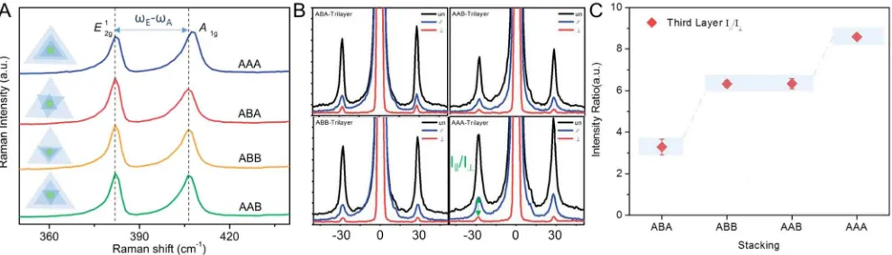
Trilayer TMD samples endows more stacking configurations and hence generate more diverse stacking-induced coupling effects. We obtained four typical stacking patterns: ABA, AAA, AAB and ABB, where the ABB and AAB atomic configurations are completely equivalent in symmetry based on our previous discus-sion[12]. As for the Raman vibration modes in the high frequency region, distinct behaviors also exhibit for trilayer system as shown inFig. 11A. The E1
2gmode almost remains unchanged while the A1g mode blue shifts with altering the 2H (ABA) stacking, leading to the largest frequency difference in AAA stacking samples (25.35 cm 1), followed by AAB (ABB) trilayer (
24.25 cm 1), and the smallest for ABA stacking (24.07 cm 1). For few-layer samples with various stacking orders, each monolayer MoS2is identical and just assembled in various sequences, leading to different lateral reg-istrations but almost identical interlayer distances. The stacking-dependent Raman feature manifests the stacking-stacking-dependent inter-layer coupling, similar with the trend on the inter-layer number [13,65,67,73]. Beyond the stacking-dependent features in high fre-quency, the ULF Raman spectra give additional information about the interlayer coupling. InFig. 11B, the SM and the BM in ULF range are merged into one peak, where Ib/Is cannot be directly used to identify the stacking configurations as in bilayer samples. Instead, we use the polarization measurements to identify the different fea-tures between the SM and BM (Ik/I\). Here, Ikis the sum of the par-allel components for both SM and BM bands, while I\contains only the perpendicular component of SM, as the BM is entirely
sup-pressed under perpendicular collection configuration. Thus, the Ik/I\ratio can be used to identify stacking configurations for trilayer systems, while Ib/Is was used for bilayer systems. As shown in Fig. 11B, the intensity ratio Ik/I\for AAA stacking is the highest, fol-lowed by AAB (ABB) stacking, with ABA stacking having the lowest ratio. We summarize the intensity ratio Ik/I\of the interlayer BM to SM for 3L MoS2(3 for ABA stacking,6 for AAB and ABB stack-ing, 8 for AAA stacking) in Fig. 11C. Beyond MoS2, stacking-dependent Raman intensities for the SM and BM are also found in other TMD materials, for instance, 3L MoSe2 as shown inFig. 12. The atomic structure (top) and displacements of the interlayer SMs (down) in ABA- and AAA-stacked 3L MoSe2 are shown inFig. 12A, similar to our previous 3L MoS2systems.Fig. 12B shows the Raman spectra of ABA- and AAA-stacked 3L CVD grown MoSe2samples. The peak around 13.3 cm 1was attributed to the lowest frequency SM (S1) in AAA-stacked 3L MoSe2, while the peak at 23.1 cm 1 corre-sponds to the theoretically predicted value of 25.5 cm 1for highest frequency SM (sN-1) in ABA-stacked 3L MoSe2[14]. The samples with both S1 and sN-1modes indicate the coexist AAA and ABA phases with either a sharp boundary[80], or a few-hundred nanometer wide transition area[81]. They also measure the sN-1Raman peak of exfoliated 3L MoSe2sample with ABA stacking and confirm that the samples that show a peak around 23.1 cm 1are ABA stacked.
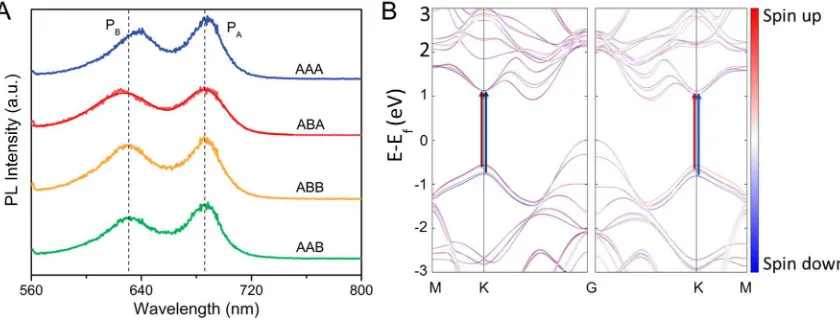
Fig. 13A plots the PL spectra of a set of 3L MoS2samples with various stackings[12]. The gray dashed lines indicate the stacking dependence of the PL peak separation between two prominent peaks PAand PB, which attribute to the direct A and B exciton tran-sitions. Interestingly, the splitting in AAA stacking samples is the Fig. 11.Stacking-dependent Raman behaviors of 3L MoS2. (A) Raman spectra of ABA-, ABB-, AAB-, AAA-stacked 3L MoS2. (B) ULF Raman of 3L MoS2with different stackings, collected under unpolarised (black)), (z(xx)z (k) (blue) and (z(xy)z (\) (red) configurations. (C) The intensity ratio of the (z(xx)z (k) and (z(xy)z (\) collection for 3L MoS2in (B) with error bars of experimental standard deviation for several samples. Reproduced with permission from Ref.[12]. Copyright 2015, American Chemical Society.
smallest (48 nm), followed by those with ABB (AAB) stacking (56 nm), while ABA stacking has the largest splitting (62 nm). Similar trend is also found in our previous 2L systems with AA and AB stacking. Such stacking-dependent splitting patterns in few-layer samples arise from the SOC and the interlayer hopping effects in TMDs. In even-layer samples with inversion symmetry, both SOC and interlayer hopping effects contribute to the splitting between A and B peaks at K points. The different behaviors in split-ting patterns have been reported in optical reflection spectra and transmission spectra for the 2H and 3R bulk phases of TMDs [11,82]. By first-principle calculation, Fig. 13B shows the spin-polarized band structures of ABA- and AAA-stacking 3L MoS2 con-sidering SOC effects. The band curves in red (blue) represent the spin-up (spin-down) states. SOC effects dominate the energy split-ting in the top valence bands for ABA-stacking, while both SOC and interlayer hopping effects contribute to the splitting patterns for AAA-stacking 3L MoS2, which corresponds to the observed stacking-dependent PL peaks separation inFig. 13A. Another inter-esting feature is the different spin-valley polarizations in different stackings: the valence band edges at K point in ABA stacking are dominantly from spin-up states with some mixing of spin-down states, while in AAA stacking, the VBM bands are completely
spin-polarized. Our ab initio calculations indicate the enhanced spin-valley polarization in the AAA stacking contrast to the ABA stacking, which is similar to the observed spin-polarized states in the 3R phase TMDs by circularly polarized photoluminescence (CP-PL) measurements[11].
Spin-valley polarization in few-layer TMDs
Following the band structure discussions for virous stacking configurations in few-layer TMDs, we then investigate how layer and stacking affect the spin and valley features. As reported, one of the most appealing applications of TMDs is the so called ‘val-leytronics’. The concept of valleys originates from that of spin and suggests the promising devices, analogous to spintronics, for next-generation electronics and optoelectronics. The key step towards valleytronics is to achieve the valley polarization through creating non-equilibrium charge carrier imbalance between K and K’ valleys [83–86]. The principal mechanism usually involved is circularly polarized optical excitation[3,4], in which the two val-leys absorb left- (
r
) and right- (r
+) hand photons respectively, leading to a valley-selective circular dichroism (CD) within a hon-eycomb lattice due to the absence of inversion symmetry. There-Fig. 12.(A) Atomic structure (top) and vibrational displacements of the interlayer shear modes (down) in ABA- and AAA- stacked 3L MoSe2. (B) Raman spectra of the 3L MoSe2with different stackings. Reproduced with permission from Ref.[14]. Copyright 2015, Nature Publishing Group.fore, in 1L TMDs without crystal inversion symmetry, the valley pseudospins can be distinguished by opposite signs at the corners (K and K’) in the hexagonal Brillouin zone. The giant SOC separates the valence bands at each valley into the spin-up and spin-down states. Such inherent spin-valley coupling can significantly protect the valley polarization as the intervalley scattering requires a simultaneous spin flip. Only carriers with selective spin can be emitted under the valley optical selection rule, which have been widely demonstrated in the literature [18,84]. The colored band structure of 1L MoS2with top valence band and bottom conduction band marked in blue and pink is shown inFig. 14A.Fig. 14B depicts the schematic of valley-dependent selection rules for monolayer TMDs at K and K0points in crystal momentum space:
r
-(r
+) circu-larly polarized light in blue (red) only couples to the band-edge transition at K (K0) points. Therefore, the direct-bandgap transition at the two degenerate valleys, together with this valley-contrasting selection rule, suggest that one can optically generate and detect valley polarizations in a TMDs monolayer[16].Beyond monolayer, few-layer TMDs introduce another intrinsic degree of freedom named as layer pseudospin. The interlayer hop-ping of electrons/holes further affects the spin–valley coupling in TMDs[21–23]. The layer pseudospin refers to the carriers’ location, either upper or lower layer in bilayer TMDs for instance. The nat-ural AB-stacked bilayer TMDs, in which the lower layer is rotated by 180°with respect to the upper layer, possess the crystal inver-sion symmetry. Consequently, the layer rotation switches two val-leys but leave the spin unchanged, which results in a sign change for the spin-valley coupling from layer to layer. In theory, the valley-dependent effect should vanish in the presence of inversion symmetry[84–86].Fig. 14C presents CP-PL spectra of thickness-dependent 3R- and 2H-MoS2 collected at 4 K with
r
excitation of 633 nm (1.96 eV), wherer
+andr
denote right and leftcircu-larly polarized light, respectively. All the spectra are composed of sharp Raman and broad PL peaks, with the latter showing a pecu-liar thickness-dependent circular polarization. For 2H stacking, the intensity difference between the
r
+andr
PL peak becomes smal-ler with increasing layer number, whereas that for 3R stacking does not show a clear layer number dependence. Therefore, thedegree of circular dichroic polarization
q
, defined as½Ið
r
Þ Iðr
þÞ=½Iðr
Þ þIðr
þÞ underr
excitation, shows obvi-ously different evolution trends versus layer number for 2H and 3R stacking TMD crystals. In summary, the valley polarizationq
in 3R MoS2 is almost independent on thickness, suggesting the strongly preserved excitons at the K (K0) point, while
q
decreases significantly in 2H MoS2.In theory, inversion-symmetric even-layer 2H-MoS2 should possess negligibly small
q
and yet the thickness-dependentq
in the 2H stacking is rather unexpected. In fact, such a noticeableq
in inversion-symmetric 2L TMDs has been widely reported in pre-vious literature[15,25]. One plausible reason is the carrier local-ized effects, where the electrons/holes are locallocal-ized in each layer rather than interlayer hopping[26]. In detail, the generated carri-ers under the circularly polarized laser (
r
orr
+) in the K (K0) val-ley tend to localize within the upper (lower) layer, and the value ofq
decreases due to the intralayer-intervalley hopping andinterlayer-intravalley hopping. However, the
interlayer-intervalley hopping should be improbable owing to the giant momentum change and layer crossing barrier. As for 3R MoS2, both interlayer and intralayer hopping are negligible and carriers are locked in each layer, leading to a larger
q
compared to that of 2H stacking. These results are also confirmed by spin- and angle-resolved photoemission spectroscopy (SARPES) inFig. 14D and E. The valence bands near the Fermi level at the K point for 2H-MoS2and 2H-WSe2are almost unpolarized. For 3R stacking cases, Fig. 14.Thickness-dependent circularly polarized PL (CP-PL) in few-layer MoS2. (A) Three-dimensional band structure of 1L MoS2with top valence band and bottom conduction band marked in blue and pink. The centre hexagon is the Brillouin zone coloured by the degree of circular polarization,q. Reproduced with permission from Ref.[85]. Copyright 2012, Nature Publishing Group. (B) Schematic of valley-dependent selection rules at K and -K points in crystal momentum space: left (right)-handed circularly polarized light in blue (red) only couples to the band-edge transition at K (-K) points (C) CP-PL spectra at 4K for 1L, 2L, 3L and 4L 2H- (left) and 3R- (right) MoS2, excited by a left circularly polarized (r) 633 nm laser. (D, E) Spin-resolved energy distribution curves (EDCs) for spin along thezaxis, collected at the inequivalent valleys of the K and -K points for 2H (D) and 3R (E) MoS2. (F, G) Calculated spin polarizations Pz/P of the valence bands along (0, ky, 0) for 2H-(F)/3R-(G) MoS2. Reproduced with permission from Ref.
In addition to valley and layer pseudospins demonstrated above, we proposed a new degree of freedom in our previous work - stacking pseudospin in 2L and 3L TMD systems, where diverse stacking configurations can be facilely grown by CVD method. Based on previous discussions, certain stacking orders can break the inversion symmetry and reduce the interlayer coupling, which are prerequisites for valley- and/or spin-selective circular dichro-ism. Among all stacking configurations, intralayer-intervalley hop-ping between the K and K0 valley is the most dominant valley relaxation path, followed by the interlayer-intravalley hopping. The latter path can preserve the momentum of the excitons and is dominated by interlayer coupling, which is in great contrast among various stackings, especially between the 2H and 3R stackings. In 2H stacking, this interlayer-intravalley hopping results in a reduction in
q
, while thisq
is not affected in the 3R stacking, as the interlayer hopping is greatly suppressed in both bilayer and bulk 3R TMDs. These results affirm that the valley polarization is robustly preserved from the interlayer hopping in the 3R-stacked TMDs, where both the interlayer and intralayerwhich the spin and valley degrees of freedom are locked within each layer owing to the broken inversion symmetry, yielding strong CD [84]. Such physical pictures are illustrated in valley and spin polarization models in 3R-like bilayers (left), as well as 2H and 2H-like bilayers (right), respectively (Fig. 15C). According to the selection rule, the 2H-like (Mo) bilayer is centrosymmetric and should exhibit unpolarized valley features[18,84], and yet still possesses a large value of valley polarization, as the interlayer hop-ping is small[17]. In natural 2H bilayers, the interlayer hopping amplitude of carries is comparable to the SOC strength, leading to mixed layer pseudospins and suppressed net spin polarization. As for the folded bilayers, interlayer coupling strength is weakened and thus the spin texture locks to the layer index, resulting in the significant CD. Similar phenomena have been found in natural 2H bilayers of WSe2(ref.[21]) and WS2(ref.[22]), in which the inter-layer hopping is suppressed owing to the giant SOC effects[20].
Our group firstly grew a series of 3L MoS2samples with various stackings and uncovered that this trilayer MoS2system also shows a strong stacking-dependent spin and valley polarizations.Fig. 16A
shows the CP-PL spectra for 3R-, AAA-, ABA (2H)- and, AAB-stacking 3L MoS2samples, which contain all the possible stacking configurations grown by CVD method[31]. Note that ABB and AAB stacking are equivalent by spatial inversion. Hence, for 3R, AAA and ABA stacking MoS2under
r
excitation at 77 K., there is only one peak situated at 1.91 eV under bothr
andr
+detection, and yet with different polarization degrees: the largest for 3R (60%), fol-lowed by AAA stacking (50%) and the smallest for ABA stacking (30%). This observation demonstrates that valley optical selection rules in 3R-MoS2 trilayer samples are consistent with previousreports [11]. Comparable with monolayer, for AAA-stacked 3L MoS2, the lack of inversion symmetry still holds, in which the spin and valley degrees of freedom are locked in AAA trilayer just like three individual monolayers, yielding strong CD. Interestingly, there are two peaks under
r
detection and one peak underr
+ detection for the ABB/AAB stacking. The energy of the correspond-ing two excitons are 1.91 eV (high energy, HE) and 1.86 eV (low energy, LE) respectively. Moreover, the HE peak displays a strong PL polarization (90%) underr
andr
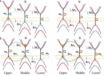
+detection, while the LE peak almost shows no spin-valley selectivity. We attribute the Fig. 16.Valley and spin polarizations in 3R-, AAA-, ABA- and, AAB-stacked 3L MoS2. (A) The CP-PL spectra from four types of 3L MoS2samples with ABB, AAB, AAA, and ABA stacking respectively. Insets: microscope images of corresponding 3L MoS2samples with four different stacking configurations. (B) Schematics of calculated electronic band structures of 3R (top) and AAB-stacked (bottom) 3L MoS2. (C) Enlarged band structure diagrams near K point for 3R- and AAB- stacked 3L MoS2. Reproduced with permission from Ref.[31]. Copyright 2016, Springer.are the mixing contributions of the upper and middle layer. The different PL polarization behaviors arise from the intrinsic stacking-modulated Bloch electrons at K(-K) valleys, as depicted inFig. 17. Here we focus on the spin textures at the band edge, which are marked with yellow rectangular blocks. The splittings between the conduction bands (Dc1, Dc2) and valence bands (Dv1, Dv2) are induced by interlayer coupling effects. Fig. 17A shows the energy level diagram of 3R-stacked 3L MoS2. The three layers are coupled with each other by reduced interlayer coupling in 3R phase, resulting in non-trivial energy splittings to form ‘triple monolayer’. The A-exciton transitions can only be excited by
r
polarized light from -K valley and the Bloch wave functions are localized in the upper layer. Due to the large energy splitting (0.1 eV), the interlayer hopping is effectively suppressed and high circular valley polarization persists similar with the monolayer case. However, in AAB-stacking trilayer, the energy levels can be treated as the mix of coupled AB bilayers and decoupled AA bilay-ers, as shown inFig. 17B. Under
r
excitation, the two detectedr
Second harmonic generation (SHG) in stacked-TMDs
Bulk MoS2 crystal with the space group D6h is inversion-symmetric which is broken when the thickness is reduced to monolayer. One consequence is to endow valley-selective optical transitions and can be used for valleytronics. It also results in non-linear optical effects, for instance, thickness-dependent optical SHG have been reported in few-layer TMDs[89–92], due to the non-trivial second-order nonlinearity associated with the broken inversion symmetry in odd few-layers. In this review, we show that this effect is highly sensitive to thickness, crystalline orienta-tion, and stacking orders.
Fig. 18A shows a MoS2sample with regions of different thick-ness for the study of thickthick-ness-dependent SHG properties. Based on the D3h symmetry, the second-order nonlinear susceptibility tensor for TMDs has the relationship of
v
(2)y0y0y0= -v
(2)y0x0x0= -v
(2)x0x0y0= -v
(2)x0y0x0=v
(2)with nonzero elements. Here, x0, y0, z0 are crystalline coordinates and x0is along the armchair direction, rotated 30°from the zigzag direction. It can be noted that the mirror symmetry isbro-Fig. 18.Thickness-dependent second harmonic generation (SHG) in few-layer MoS2. (A) Microscope image of a mechanically exfoliated MoS2flake with layer thickness from 1L to 4 L. (B) Lattice structure of 1L MoS2. Mo and S atoms are depicted as blue and yellow balls. (C) The normalized PL spectra of the signals from SHG in 1L MoS2(blue), the fundamental laser (red), and the pure substrate (gray, multiplied by a factor of 100). (D) The power of parallel (blue squares) and perpendicular (black circles) components of the SHG as a function ofh, the angle between the laboratory and the crystalline coordinates. The blue (black) solid line illustrates the theoretical sin23h(cos23h) relationship. (E) The second harmonic power measured from different regions with layer number varying from 1L to 4L. Reproduced with permission from Ref.[34]. Copyright 2013 American Physical Society. (F) White-light image and SHG mapping of a CVD grown 1 L MoS2, respectively. The scale bars are 10lm. Reproduced with permission from Ref.
ken along zigzag direction, as shown in the lattice structure diagram of 1L MoS2(Fig. 18B). It has been proven that the parallel (x) and perpendicular (y) components of the SHG field are proportional to sin(3u) and cos(3u), respectively, whereuis the angle between inci-dent laser polarization direction (x) and the armchair direction in crystalline coordinates (x0). Hence, the power can be expressed as Px/sin2(3u) and Py/cos2(3u), while the total power (P = Px+ Py) is independent ofu[34].
In the SHG experiments, the fundamental excitation pulse from a Ti-Sapphire laser centered at 810 nm is tightly focused to a spot of 2
l
m in diameter, in the normal incident (along z0) geometry and linearly polarized along the horizontal direction (defined as x in the laboratory coordinates), as shown inFig. 18A. As the photon energy of 810 nm laser is less than the bandgap of the sample, res-onant band-to-band absorption of the fundamental excitation light is not considered.Fig. 18C shows the normalized SHG spectrum from the 1L MoS2(blue) region and the substrate (gray), together with that of the fundamental laser beam (red), and. The SHG inten-sity contrast of the 1L MoS2with respect to the substrate is more than 104, which is much higher than that for linear PL signal (only about 0.3), where SHG signal shows expected quadratic depen-dence on the excitation power. The parallel (Px) and perpendicular (Py) components of the SHG were measured as a function ofuas shown inFig. 18D. The blue [black] solid line depicts the theoreti-cal sin2(3u) [cos2(3u)] relationship from the D3h symmetry. Through this u-dependent SHG of the Pxand Py, the magnitude ofv
(2)in 1L MoS2can be estimated to be around 10 7m/V by solv-ing the coupled-wave equations[32]. As a result, the 1L MoS2 pos-sesses a largev
(2), which vanishes in bilayer 2H-MoS2. Therefore, the investigation of how
v
(2)varies with the number of atomic lay-ers shows great significance. The total power of the SHG from dif-ferent layer regions of the MoS2flake are summarized inFig. 18E, with a fixed excitation power of 4 mW. Since the total power is independent ofu, the measurement will not be affected by the dif-ferent crystal orientations within these regions. It has been found thatv
(2)of the 3L sample is about a factor of seven smaller than that in the 1L sample, while those in the 2L and 4L MoS2are about three orders of magnitude smaller. As TMD flakes with an even number of layers possess inversion symmetry, their second-order response should vanish theoretically. The smaller but nonzerov
(2)observed in experiments can be possibly attributed to surface and interface effects. A similar layer-number dependence has also been observed recently in WS2and WSe2[35]. The bulk MoS2 crys-tal (2H) shows its SHG power is about five orders of magnitude smaller than its monolayer counterpart, which stems from the inversion symmetry[34].SHG microscopy has been utilised to visualize the edge termi-nation (Mo vs S) of grain boundaries and the crystalline orienta-tions (Mo–S vs S–Mo) in as grown 1L MoS2, owing to its high sensitivity to structural symmetry [9,34,36]. This non-invasive optical technique with high output is generally applicable to a wide range of 2D materials besides TMDs [93], including BN [94,95], GaSe [95] and other hybrid structures [53,96]. Through mapping out a large amount of 1L MoS2samples with diverse ori-entation distributions, an understanding of grain growth and boundary formation through statistical analyses has been estab-lished. It has been found that the grain boundary formation in TMDs is driven by kinetics, without showing any preference for energetically favored structures. Fig. 18F (left image) shows the optical microscopic image of the 1L MoS2samples grown on sap-phire substrate by low-pressure CVD. It is covered by MoS2 trian-gles of the same optical contrast and all edges are straight. While the sample shows uniform contrast in the white-light image, the polarized SHG mapping of the same area indicates that it is formed by many MoS2 triangular grains with different orientations
(Fig. 18F-right), where sharp boundaries exist between adjacent triangular grains. The contrast of various grains is originated from the anisotropic SHG response of 1 L MoS2 as described before. Briefly, when incident and collected lights are linearly polarized along the same direction, the SHG intensity is the largest when the direction of laser polarization is perfectly aligned to the arm-chair directions in 1L MoS2. Therefore, by measuring the SHG ani-sotropic polarization patterns, the lattice orientations of all domains relative to the laser polarization can be readily deter-mined, and hence the triangle edges with reduced SHG intensity can be predominantly identified as zigzag terminated by either Mo or S atoms[97].
Few-layer TMD samples also show strong stacking dependence in SHG response. The presence or absence of an inversion symme-try in bilayer TMDs with different stacking endows various second-order optical nonlinearity and this stacking angle dependence of the SHG can be utilised. Hsu et al. [39] have investigated the SHG from artificially stacked bilayer MoS2 with different twist angles, in which the signal is a coherent superposition of the SH fields within each layer with a phase difference due to the stacking angle. They investigated a bilayer MoS2with a rotation angle of h= 25°between the 2 layers inFig. 19A. A back-reflection geome-try is adopted and the pump laser was incident normally on the sample with its electric field along the x direction, parallel with the armchair direction of the 1L Flake 1 (Fig. 19B). In this configu-ration, this SHG intensity is maximum for 1L Flake 1. Based on the polar plots of the polarization-resolved SHG intensity as a function of theuas shown inFig. 19D and E, the individual 1L flake shows a six-petal feature, in which the petals lie along the perpendicular bisectors of each flake. The SHG signal for the 2L stacking region (Fig. 19F) also shows a six-petal pattern with its maximum signal lying in the middle of that of Flakes 1 and Flake 2. The SHG signal for the 2L region can be explained as the coherently interfered response between the two 1L flakes. The net SH electric field Es(2
x
) in the 2L region can be expressed using a vector superposi-tion:Es(2x
)=E1(2x
)+E2(2x
). The total SHG intensity in the stack-ing region is proportional to |Es(2x
)|2, which can be described as IsðhÞ ¼I1þI2þ2pIffiffiffiffiffiffiffiffi1I2cos 3h, where Is, I1, and I2stand for the SHG intensity in the 2L stacking region, the 1L Flake 1 and Flake 2 respectively; andh(=25°in this case) is the stacking angle between layers (Fig. 19C).Fig. 20shows a series of 2L MoS2with various stacking angles (2°, 16°, 30°, 37°, 54°) and the corresponding SHG intensity mappings. It has been proven that the SHG intensity in the bilayer region strongly dependent on the stacking angle. Based on the equation above, the SHG intensity varies as cos3h, which gives Is(h= 0°) = 4I0 (fully constructive) to Is(h= 60°) = 0 (fully destructive) as the SH intensity from each flake is the same. There-fore, SHG also provides an efficient characterization tool for stack-ing orientation in bilayer TMDs system[39].sam-ple with 0.83 nm thickness and lateral side length of15
l
m on mica substrate. The prominent PL peaks at 675 nm and 450 nm correspond to the SHG and third-harmonic-generation (THG) sig-nals, respectively. 1L GaSe has a bandgap of2.3 eV, corresponding to a 540 nm laser excitation[95,100]. Similar to MoS2, 1L GaSe belongs to noncentrosymmetric D13h space group and therefore has nonzero SHG signal[37,101]. The 2L GaSe possess two stacking sequences: AA and AB stacking, where the relative atomic
arrange-ments between layers are shown in Fig. 21B. In AA stacking, the in-plane Ga-Se bond direction is the same for the two layers, while in the AB-stacking, the Ga-Se bond direction is opposite. AA-stacking 2L GaSe still belongs to noncentrosymmetric D1
3hgroup as in 1L and therefore, should have a strong SHG signal. The electric dipole theory predicts that the SHG signal in AA-stacked bilayer is four times that of the 1L (the SHG signals from two layers are con-structive). In contrast, AB-stacking bilayer belongs to the centrosym-Fig. 19.Stacking-dependent SHG in artificially stacked 2L MoS2. (A) The optical image of a 2L MoS2with a stacking angle ofh= 25°. (B) The schematic illustration of incident laser polarization in terms of the measured SHG polarization. The azimuthal angleuis defined as the angle between the laser polarization and the armchair direction of the monolayer flake in (A). (C) A schematic for illustrating the vector superposition of the SH electric fields (a), where E(x) is the electric field of the incident laser, E1(2x) and E2(2x) are the generated SH electric field from the monolayer flake 1 (flake 2), and Es(2x) is the resulting SH electric field from the 2 L stacking region. (b-d) Schematics for stacked bilayers with (b) an arbitrary stacking angleh, 0°, 60°, 180°. (D–F) Polar plots of the polarization-resolved SH intensity as a function ofumeasured from the 1L region (1) (D), 1L region (2) (E), and 2L stacking region (F). Reproduced with permission from Ref.[10,39]. Copyright 2014, American Chemical Society.
metric D1
3dgroup and, therefore, has no appreciable SHG signal (the SHG signals from two layers are destructive). Therefore, in the SHG mappings, we observed that AA stacking (0°) bilayer gives rise to enhanced SHG signal (Fig. 21D), while the AB stacking (60°) bilayer gives nearly zero SHG signal (Fig. 21F).[102].
Thickness and phase engineered TMD electronic devices
The nature of TMDs, such as the appropriate bandgap, high carrier mobility, high current on/off ratios and thickness-/ phase-dependent energy band structure, makes TMDs as the ideal semiconductor material for the field-effect transistors (FETs), pho-tovoltaics, photodetectors, and nonvolatile memories. A series of thickness-dependent homojunctions are fabricated based on
1L-2L, 2L-3L, and 3L-4L MoSe2, as illustrated in Fig. 22. The 1L-2L homojunction shows the current rectification behaviors, in which the monolayer MoSe2acts as the cathode and the bilayer MoSe2 as the anode. By applying a forward source-drain bias (Vds) of 10 V, 0.1 nA current goes through the device, while a small current ( 0.0023 nA) is emerged with a reverse Vdsof 10 V. The on-off ratio for this 1L-2L MoSe2device can be expressed as Iforward/Ireversewith the value of 81, demonstrating a good current rectification feature. The thicker 2L-3L and 3L-4L junctions give rise to a smaller current rectification ratio. The calculated band structures have been per-formed to elucidate the thickness-dependent rectification behav-iors. In the 1L-2L junction, type II band alignment is formed between the conduction band minimum located in the 1L region and the valance band maximum situated in the 2L with a band off-Fig. 22.Thickness-dependent current rectification behaviors in MoSe2homojunctions. (A) Optical image of the devices based on intrinsic junctions in MoSe2formed by 1L-2L and 2L-3L domains. (B, C) Output characteristics (Ids-Vdscurves) of MoSe2electronic devices based on 1L-2L (B) and 2L-3L (C) junctions. Both show a typical diode behaviors. Reproduced with permission from Ref.[47]. Copyright 2016 John Wiley and Sons.
set of0.4 eV, leading to a built-in electric field pointing from the 2L to the 1L. The corresponding band offset in thicker junctions is decreased compared to that of 1L-2L junction, e.g., 2L-3L junction with a band offset of 0.2 eV, resulting in a lower current rectification ratio as demonstrated above [49]. Such homojunc-tions provide a useful alternative for designing and fabricating electronic devices.
Phase-engineered FETs have been fabricated by direct self-assembly patterning of few-layer MoS2, through directional semiconducting-to-metallic phase transition method. Two types of MoS2FET devices are illustrated inFig. 23A and B. One is con-structed on exfoliated 3L MoS2 with 7.5 nm channel length and the other is fabricated by alternating 2H/1T0 MoS2 regions pro-duced after a phase transition treatment with n-butyllithium (nBuLi). For all FET devices, highly doped Si substrates with a 10 nm of HfO2layer on the surface are used as the backgate stacks. Fig. 23C and E show the transfer (Ids-Vgs) and output (Ids-Vds) char-acteristics of the pure 3L 2H-MoS2FETs, where the as-fabricated device with channel length of 90 nm shows good subthreshold characteristics with a small drain-induced barrier lowering (DIBL < 0.1 V/V), subthreshold swing (SS) = 88 mV/dec, and current saturation in Ids-Vdscharacteristics caused by velocity saturation. However, for the 2H/1T0 MoS2 chain (7.5 nm) FETs, the devices demonstrate a well-defined Ids-Vgs with an on–off ratio (Ion/Ioff) of107, Ioffof
10 pA/
l
m, Ionof 0.25 mA/l
m and a subthreshold slope of 120 mV/dec for more than two decades (Fig. 23D). Due to the extremely thin body thickness and the wide bandgap of the MoS2, the short channel length of this device has a minimum impact on its subthreshold characteristics and the off-state current (low Ioffof10 pA/l
m). Compared with the Ids-Vgscharacteristics of the long channel (Fig. 23C), the chain FET device shows larger DIBL of 0.7 V/V. This also leads to the nonsaturation in the Ids-Vdscurves (Fig. 23F) despite the higher current density in the mA/l
m range compared with the pure 3L MoS2FETs. Throughfit-ting the experimental data (the device current-voltage characteris-tics) for the MoS2FETs by MIT Virtual Source Compact model, the device parameters such as injection velocity, carrier mobility, and the 2H/1T0junction resistance can be extracted. The 2H/1T0 junc-tion resistivity is identified as low as 75X
l
m that indicates the ohmic contact nature of the 2H/1T0 junction, while pure 3L 2H-MoS2FETs exhibit a low-field mobility of25 cm2/V s and a carrier injection velocity of106cm/s. The low Ioffand high Ion/Ioffresult from the ability of MoS2to suppress direct source-drain tunneling owing to its high effective mass. These results highlight the promise of MoS2transistors fabricated on the basis of phase engi-neering [103]. In analogy, the thickness-/phase-engineered and stacking-dependent properties in other TMD materials and devices should also exhibit novel electronic and optoelectronic properties.
Conclusion
In summary, the research on the physical properties and appli-cations of thickness- and stacking-engineered TMDs is of great sig-nificance and has attracted intensive attention. As an outlook of this review, controllable and productive growth of layered TMDs with desired stacking orientations will play an important role for further physical study and future applications of TMDs-based devices. For instance, one can investigate the excitons dynamics in stacking-engineered TMDs by time-resolved photoluminescence or electroluminescence. Besides thickness-dependent TMD homo-junctions demonstrated above, there should be more intriguing electronic and optoelectronic responses for stacking-engineered TMD junctions with both lateral and vertical interface.
Acknowledgements
2 (MOE2015-T2-1-148) and AcRF Tier 3 (MOE2011-T3-1-005) in Cronin, D. Smirnov, M. Koshino, E. McCann, M. Bockrath, C.N. Lau, Nat. Phys. 7 (2011) 948–952.
[5]Z. Liu, M. Amani, S. Najmaei, Q. Xu, X. Zou, W. Zhou, T. Yu, C. Qiu, A.G. Birdwell, F.J. Crowne, R. Vajtai, B.I. Yakobson, Z. Xia, M. Dubey, P.M. Ajayan, J. Lou, Nat. Commun. 5 (2014) 5246.
[6]Z. Zhao, H. Zhang, H. Yuan, S. Wang, Y. Lin, Q. Zeng, G. Xu, Z. Liu, G.K. Solanki, K.D. Patel, Y. Cui, H.Y. Hwang, W.L. Mao, Nat. Commun. 6 (2015) 7312. [7]J. He, K. Hummer, C. Franchini, Phys. Rev. B 89 (2014).
[8]M.N. Ali, J. Xiong, S. Flynn, J. Tao, Q.D. Gibson, L.M. Schoop, T. Liang, N. Haldolaarachchige, M. Hirschberger, N.P. Ong, R.J. Cava, Nature 514 (2014) 205–208.
[9]T. Jiang, H. Liu, D. Huang, S. Zhang, Y. Li, X. Gong, Y.R. Shen, W.T. Liu, S. Wu, Nat. Nano. 9 (2014) 825–829.
[10]W.T. Hsu, Z. Zhao, L.J. Li, C.H. Chen, M.H. Chiu, P.S. Chang, Y.C. Chou, W.H. Chang, ACS Nano 8 (2014).
[11]R. Suzuki, M. Sakano, Y.J. Zhang, R. Akashi, D. Morikawa, A. Harasawa, K. Yaji, K. Kuroda, K. Miyamoto, T. Okuda, K. Ishizaka, R. Arita, Y. Iwasa, Nat. Nano. 9 (2014) 611–617.
[12]J. Yan, J. Xia, X. Wang, L. Liu, J.L. Kuo, B.K. Tay, S. Chen, W. Zhou, Z. Liu, Z.X. Shen, Nano Lett. 15 (2015) 8155–8161.
[13]M. Boukhicha, M. Calandra, M.-A. Measson, O. Lancry, A. Shukla, Phys. Rev. B 87 (2013).
[21]A.M. Jones, H. Yu, J.S. Ross, P. Klement, N.J. Ghimire, J. Yan, D.G. Mandrus, W. Yao, X. Xu, Nat. Phys. 10 (2014) 130–134.
[25]G. Aivazian, Z. Gong, A.M. Jones, R.-L. Chu, J. Yan, D.G. Mandrus, C. Zhang, D. Cobden, W. Yao, X. Xu, Nat. Phys. 11 (2015) 148–152.
[26]X. Li, F. Zhang, Q. Niu, Phys. Rev. Lett. 110 (2013) 066803.
[27]T. Scrace, Y. Tsai, B. Barman, L. Schweidenback, A. Petrou, G. Kioseoglou, I. Ozfidan, M. Korkusinski, P. Hawrylak, Nat. Nano. 10 (2015) 603–607. [28]D. MacNeill, C. Heikes, K.F. Mak, Z. Anderson, A. Kormanyos, V. Zolyomi, J.
Park, D.C. Ralph, Phys. Rev. Lett. 114 (2015) 037401.
[29]R. Akashi, M. Ochi, S. Bordács, R. Suzuki, Y. Tokura, Y. Iwasa, R. Arita, Phys. Rev. Applied 4 (2015).
[30]A. Splendiani, L. Sun, Y. Zhang, T. Li, J. Kim, C.Y. Chim, G. Galli, F. Wang, Nano Lett. 10 (2010) 1271–1275.
[31]J. Xia, X. Wang, B.K. Tay, S. Chen, Z. Liu, J. Yan, Z. Shen, Nano Res. (2016). [32]R. Boyd, Nonlinear Optics, 3rd Ed., Academic Press, Burlington, 2008, pp.
xiii–xiv.
[33]G.A. Wagoner, P.D. Persans, E.A. Van Wagenen, G.M. Korenowski, J. Opt. Soc. Am. B 15 (1998) 1017–1021.
[34]N. Kumar, S. Najmaei, Q. Cui, F. Ceballos, P.M. Ajayan, J. Lou, H. Zhao, Phys. Rev. B 87 (2013).
[35]H. Zeng, G.B. Liu, J. Dai, Y. Yan, B. Zhu, R. He, L. Xie, S. Xu, X. Chen, W. Yao, X. Cui, Sci. Rep. 3 (2013) 1608.
[36]L.M. Malard, T.V. Alencar, A.P.M. Barboza, K.F. Mak, A.M. de Paula, Phys. Rev. B 87 (2013) 201401.
[37]Y. Li, Y. Rao, K.F. Mak, Y. You, S. Wang, C.R. Dean, T.F. Heinz, Nano Lett. 13 (2013) 3329–3333.
[38]C.-J. Kim, L. Brown, M.W. Graham, R. Hovden, R.W. Havener, P.L. McEuen, D.A. Muller, J. Park, Nano Lett. 13 (2013) 5660–5665.
[39]W.-T. Hsu, Z.-A. Zhao, L.-J. Li, C.-H. Chen, M.-H. Chiu, P.-S. Chang, Y.-C. Chou, W.-H. Chang, ACS Nano 8 (2014) 2951–2958.
[40]E.O. Ortiz-Quiles, C.R. Cabrera, FlatChem. 2 (2017) 1–7. [41]Q. Van Le, J.-Y. Choi, S.Y. Kim, FlatChem. 2 (2017) 54–66.
[42]O. Lopez-Sanchez, D. Lembke, M. Kayci, A. Radenovic, A. Kis, Nat. Nano. 8 (2013) 497–501.
[43]D. Sarkar, W. Liu, X.J. Xie, A.C. Anselmo, S. Mitragotri, K. Banerjee, ACS Nano 8 (2014).
[44]H.M. Li, D.Y. Lee, M.S. Choi, D. Qu, X. Liu, C.H. Ra, W.J. Yoo, Sci. Rep. 4 (2014) 4041.
[45]D. Li, R. Cheng, H. Zhou, C. Wang, A. Yin, Y. Chen, N.O. Weiss, Y. Huang, X. Duan, Nat. Commun. 6 (2015) 7509.
[46]H. Schmidt, F. Giustiniano, G. Eda, Chem. Soc. Rev. 44 (2015) 7715–7736. [47]X. Xu, N.M. Gabor, J.S. Alden, A.M. van der Zande, P.L. McEuen, Nano Lett. 10
(2010) 562–566.
[48]S.L. Howell, D. Jariwala, C.C. Wu, K.S. Chen, V.K. Sangwan, J. Kang, T.J. Marks, M.C. Hersam, L.J. Lauhon, Nano Lett. 15 (2015) 2278–2284.
[49]Y. He, A. Sobhani, S. Lei, Z. Zhang, Y. Gong, Z. Jin, W. Zhou, Y. Yang, Y. Zhang, X. Wang, B. Yakobson, R. Vajtai, N.J. Halas, B. Li, E. Xie, P. Ajayan, Adv. Mater. (2016). [50] Y. Katagiri, T. Nakamura, A. Ishii, C. Ohata, M. Hasegawa, S. Katsumoto, T. Cusati, A. Fortunelli, G. Iannaccone, G. Fiori, S. Roche, J. Haruyama, Nano Lett. 16 (2016) 3788–3794. Yakobson, H. Terrones, M. Terrones, B.K. Tay, J. Lou, S.T. Pantelides, Z. Liu, W. Zhou, P.M. Ajayan, Nat. Mater. 13 (2014) 1135–1142.
[54]N. Huo, Z. Wei, X. Meng, J. Kang, F. Wu, S.-S. Li, S.-H. Wei, J. Li, J. Mater. Chem. C 3 (2015) 5467–5473.
[55]J.M. Woods, Y. Jung, Y. Xie, W. Liu, Y. Liu, H. Wang, J.J. Cha, ACS Nano 10 (2016) 2004–2009.
[56]M.Y. Li, Y. Shi, C.C. Cheng, L.S. Lu, Y.C. Lin, H.L. Tang, M.L. Tsai, C.W. Chu, K.H. Wei, J.H. He, W.H. Chang, K. Suenaga, L.J. Li, Science 349 (2015).
[57]K.S. Novoselov, A.H. Castro Neto, Phys. Scr. T146 (2012) 014006.
[58]Z. Zeng, Z. Yin, X. Huang, H. Li, Q. He, G. Lu, F. Boey, H. Zhang, Angew. Chem. Int. Ed. 50 (50) (2011) 11093–11097.
[59]Y.-H. Lee, X.-Q. Zhang, W. Zhang, M.-T. Chang, C.-T. Lin, K.-D. Chang, Y.-C. Yu, J.T.-W. Wang, C.-S. Chang, L.-J. Li, T.-W. Lin, Adv. Mater. 24 (2012) 2320–2325. [60] J.-G. Song, J. Park, W. Lee, T. Choi, H. Jung, C.W. Lee, S.-H. Hwang, J.M. Myoung, J.-H. Jung, S.-H. Kim, C. Lansalot-Matras, H. Kim, ACS Nano 7 (2013) 11333– 11340.
[61]G. Fiori, F. Bonaccorso, G. Iannaccone, T. Palacios, D. Neumaier, A. Seabaugh, S. K. Banerjee, L. Colombo, Nat. Nano. 9 (2014) 768–779.
[62]W. Zhang, J. Yan, C.-H. Chen, L. Lei, J.-L. Kuo, Z. Shen, L.-J. Li, Nat. Commun. 4 (2013) 2074.
[63]Y. Lee, D. Tran, K. Myhro, J. Velasco, N. Gillgren, C.N. Lau, Y. Barlas, J.M. Poumirol, D. Smirnov, F. Guinea, Nat. Commun. 5 (2014) 5656.
[64]M.F. Craciun, S. Russo, M. Yamamoto, J.B. Oostinga, A.F. Morpurgo, S. Tarucha, Nat. Nano 4 (2009) 383–388.
[65]X. Luo, Y. Zhao, J. Zhang, Q. Xiong, S.Y. Quek, Phys. Rev. B 88 (2013). [66]Y. Zhao, X. Luo, H. Li, J. Zhang, P.T. Araujo, C.K. Gan, J. Wu, H. Zhang, S.Y. Quek,
M.S. Dresselhaus, Q. Xiong, Nano Lett. 13 (2013) 1007–1015. [67]A. Molina-Sánchez, L. Wirtz, Phys. Rev. B 84 (2011).
[68]K.F. Mak, K. He, C. Lee, G.H. Lee, J. Hone, T.F. Heinz, J. Shan, Nat. Mater. 12 (2013) 207–211.
[69]K.F. Mak, C. Lee, J. Hone, J. Shan, T.F. Heinz, Phys. Rev. Lett. 105 (2010) 136805. [70] K.P. Dhakal, D.L. Duong, J. Lee, H. Nam, M. Kim, M. Kan, Y.H. Lee, J. Kim,
Nanoscale 6 (2014) 13028–13035.
[71]M. O’Brien, N. McEvoy, D. Hanlon, T. Hallam, J.N. Coleman, G.S. Duesberg, Sci. Rep. 6 (2016) 19476.
[72]A.A. Puretzky, L. Liang, X. Li, K. Xiao, K. Wang, M. Mahjouri-Samani, L. Basile, J. C. Idrobo, B.G. Sumpter, V. Meunier, D.B. Geohegan, ACS Nano 9 (2015) 6333– 6342.
[73]X. Zhang, W.P. Han, J.B. Wu, S. Milana, Y. Lu, Q.Q. Li, A.C. Ferrari, P.H. Tan, Phys. Rev. B 87 (2013).
[74]K. Liu, L. Zhang, T. Cao, C. Jin, D. Qiu, Q. Zhou, A. Zettl, P. Yang, S.G. Louie, F. Wang, Nat. Commun. 5 (2014) 4966.
[75]C. Lee, H. Yan, L.E. Brus, T.F. Heinz, J. Hone, S. Ryu, ACS Nano 4 (2010) 2695– 2700.
[76]F.J. Crowne, M. Amani, A.G. Birdwell, M.L. Chin, T.P. O’Regan, S. Najmaei, Z. Liu, P.M. Ajayan, J. Lou, M. Dubey, Phys. Rev. B 88 (2013) 235302. [77]A. Castellanos-Gomez, H.S.J. van der Zant, G.A. Steele, Nano Res. 7 (2014)
572–578.
[78]W. Zhao, R.M. Ribeiro, M. Toh, A. Carvalho, C. Kloc, A.H. Castro Neto, G. Eda, Nano Lett. 13 (2013) 5627–5634.
[79]Y. Zhang, T.-R. Chang, B. Zhou, Y.-T. Cui, H. Yan, Z. Liu, F. Schmitt, J. Lee, R. Moore, Y. Chen, H. Lin, H.-T. Jeng, S.-K. Mo, Z. Hussain, A. Bansil, Z.-X. Shen, Nat. Nano 9 (2014) 111–115.
[80] X. Lu, M.I.B. Utama, J. Lin, X. Gong, J. Zhang, Y. Zhao, S.T. Pantelides, J. Wang, Z. Dong, Z. Liu, W. Zhou, Q. Xiong, Nano Lett. 14 (2014) 2419–2425. [81]X. Lu, M.I.B. Utama, J. Lin, X. Luo, Y. Zhao, J. Zhang, S.T. Pantelides, W. Zhou, S.
Y. Quek, Q. Xiong, Adv. Mater. 27 (2015) 4502–4508.
[82]M. Xia, B. Li, K. Yin, G. Capellini, G. Niu, Y. Gong, W. Zhou, P.M. Ajayan, Y.-H. Xie, ACS Nano 9 (2015) 12246–12254.
[83]A. Rycerz, J. Tworzydlo, C.W.J. Beenakker, Nat. Phys. 3 (2007) 172–175. [84]W. Yao, D. Xiao, Q. Niu, Phys. Rev. B 77 (2008) 235406.
[85]O. Gunawan, Y.P. Shkolnikov, K. Vakili, T. Gokmen, E.P. De Poortere, M. Shayegan, Phys. Rev. Lett. 97 (2006) 186404.
[86]Z. Zhu, A. Collaudin, B. Fauque, W. Kang, K. Behnia, Nat. Phys. 8 (2012) 89–94. [87]T. Cao, G. Wang, W. Han, H. Ye, C. Zhu, J. Shi, Q. Niu, P. Tan, E. Wang, B. Liu, J.
Feng, Nat. Commun. 3 (2012) 887.
[96]C. Huang, S. Wu, A.M. Sanchez, J.J.P. Peters, R. Beanland, J.S. Ross, P. Rivera, W. Yao, D.H. Cobden, X. Xu, Nat. Mater. 13 (2014) 1096–1101.