LM139, LM239, LM339
Low-power quad voltage comparators
Features
■ Wide single supply voltage range or dual supplies for all devices: +2 to +36 V or ±1 V to ±18 V
■ Very low supply current (1.1 mA) independent of supply voltage
■ Low input bias current: 25 nA typ
■ Low input offset current: ±5 nA typ
■ Low input offset voltage: ±1 mV typ
■ Input common-mode voltage range includes ground
■ Low output saturation voltage: 250 mV typ; (ISINK = 4 mA)
■ Differential input voltage range equal to the supply voltage
■ TTL, DTL, ECL, MOS, CMOS compatible outputs
Description
This family of devices consists of four
independent precision-voltage comparators with an offset voltage specification as low as 2 mV maximum for LM339A, LM239A and LM139A. Each comparator has been designed specifically to operate from a single power supply over a wide range of voltages. Operation from split power supplies is also possible.
These comparators also have a unique characteristic in that the input common mode voltage range includes ground even though operated from a single power supply voltage.
N DIP14 (Plastic package)
D SO-14 (Plastic micropackage)
P TSSOP14
(Thin shrink small outline package)
Q QFN16 3x3 (Plastic micropackage)
July 2011 Doc ID 2159 Rev 3 1/19
www.st.com 19
Pin and schematic diagram LM139, LM239, LM339
1
Pin and schematic diagram
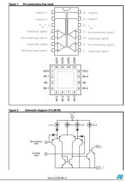
Figure 1. Pin connections (top view)
Output2 1
Output1 2
V + CC
3
14 Output3
13 Output4
12
11
10
9
8 V
CC -
Inverting input1
Non-inverting input1
Inverting input2
Non-inverting input2 4
5
6
7
Non-inverting input4
Inverting input4
Non-inverting input3
Inverting input3
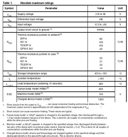
Figure 2. Schematic diagram (1/4 LM139)
VCC
3.5A 100A 3.5A 100A
Non-inverting input
V
O
Inverting input
V
CC
2/19 Doc ID 2159 Rev 3
LM139, LM239, LM339 Absolute maximum ratings and operating conditions
2
Absolute maximum ratings and operating conditions
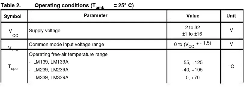
Table 1.
Absolute maximum ratings Parameter
Supply voltage
Differential input voltage
Input voltage
Output short-circuit to ground (1) Thermal resistance junction to ambient(2)
DIP14 SO-14 TSSOP14 QFN16 3x3
Thermal resistance junction to case (2) DIP14
SO-14 TSSOP14 QFN16 3x3
Storage temperature range
Junction temperature
Lead temperature (soldering 10 seconds)
Human body model (HBM)(3) Machine model (MM)(4) Charged device model (CDM)(5)
Value
1. Short-circuits from the output to VCC + can cause excessive heating and eventual destruction. The maximum output current is approximately 20 mA independent of the magnitude of VCC +. 2. Short-circuits can cause excessive heating. These values are typical.
3. Human body model: a 100 pF capacitor is charged to the specified voltage, then discharged through a 1.5 kΩ resistor between two pins of the device. This is done for all couples of connected pin combinations while the other pins are floating.
4. Machine model: a 200 pF capacitor is charged to the specified voltage, then discharged directly between two pins of the device with no external series resistor (internal resistor < 5Ω). This is done for all couples of connected pin combinations while the other pins are floating.
5. Charged device model: all pins and the package are charged together to the specified voltage and then discharged directly to the ground through only one pin. This is done for all pins.
Doc ID 2159 Rev 3 3/19
Absolute maximum ratings and operating conditions LM139, LM239, LM339
Table 2.
Symbol
V CC
VICM
Operating conditions (Tamb
Parameter
Supply voltage
Common mode input voltage range
= 25° C)
Value
2 to 32 ±1 to ±16
0 to (VCC + - 1.5)
Unit
V
V
Toper
Operating free-air temperature range - LM139, LM139A
- LM239, LM239A - LM339, LM339A
-55, +125 -40, +105 0, +70
°C
4/19 Doc ID 2159 Rev 3
LM139, LM239, LM339 Electrical characteristics
3
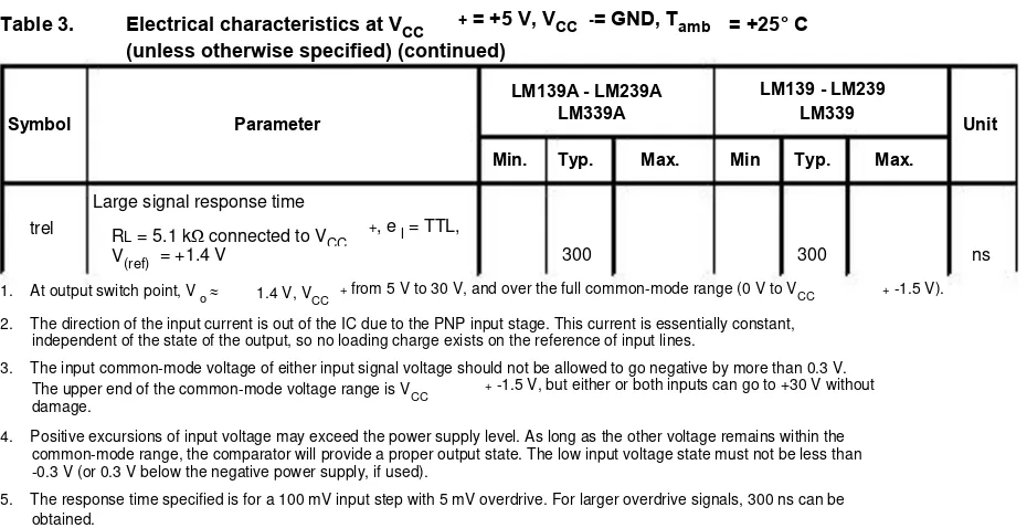
Table 3.
Electrical characteristics
Electrical characteristics at VCC (unless otherwise specified)
+ = +5 V, VCC -= GND, Tamb = +25° C
Input offset voltage (1) TminTambTmax Input offset current
TminTambTmax Input bias current (I + or I )
TminTambTmax Large signal voltage gain
VCC = 15 V, R L = 15 kΩ
Supply current (all comparators) VCC
Input common mode voltage range (3) VCC = 30 V
TminTambTmax Differential input voltage (4) Low level output voltage
VID = -1 V, ISINK =
High level output current VCC
Output sink current
ID= 1 V, V o = 1.5 V
Electrical characteristics LM139, LM239, LM339
Table 3. Electrical characteristics at VCC + = +5 V, VCC -= GND, Tamb = +25° C
(unless otherwise specified) (continued)
LM139A - LM239A Parameter
Min.
LM339A Typ.
LM139 - LM239 LM339 Min Typ. Max.
Symbol Unit
Max.
Large signal response time
RL = 5.1 kΩ connected to VCC
trel +, e l = TTL,
V(ref) = +1.4 V 300 300 ns
1. At output switch point, V o 1.4 V, VCC + from 5 V to 30 V, and over the full common-mode range (0 V to VCC + -1.5 V). 2. The direction of the input current is out of the IC due to the PNP input stage. This current is essentially constant,
independent of the state of the output, so no loading charge exists on the reference of input lines.
3. The input common-mode voltage of either input signal voltage should not be allowed to go negative by more than 0.3 V. The upper end of the common-mode voltage range is VCC
damage.
+ -1.5 V, but either or both inputs can go to +30 V without
4. Positive excursions of input voltage may exceed the power supply level. As long as the other voltage remains within the common-mode range, the comparator will provide a proper output state. The low input voltage state must not be less than -0.3 V (or 0.3 V below the negative power supply, if used).
5. The response time specified is for a 100 mV input step with 5 mV overdrive. For larger overdrive signals, 300 ns can be obtained.
6/19 Doc ID 2159 Rev 3
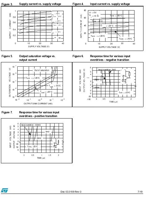
LM139, LM239, LM339 Electrical characteristics curves
4
Figure 3.
Electrical characteristics curves
Supply current vs. supply voltage Figure 4.
80
60
40
20
Input current vs. supply voltage
1
Figure 5. Output saturation voltage vs. output current
Figure 6.
1 10
Response time for various input overdrives - negative transition
6 Out of saturation
0 OUTPUT SINK CURRENT (mA)
Figure 7. Response time for various input overdrives - positive transition
20mV
Input overdrive : 100mV
5mV
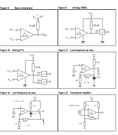
Typical applications LM139, LM239, LM339
5
Figure 8.
Typical applications
Basic comparator
VCC = 5 V
Figure 13. Transducer amplifier
5 V
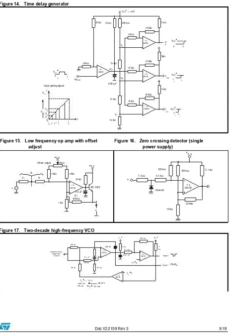
LM139, LM239, LM339 Typical applications Input gating signal
VCC
Figure 16. Zero crossing detector (single power supply)
Figure 17. Two-decade high-frequency VCO
V
CC 100 kΩ
VCC
100 kΩ
Frequency control voltage input
Vcontrol
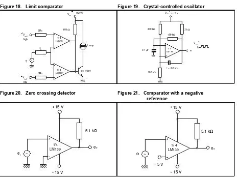
Typical applications LM139, LM239, LM339
Figure 18. Limit comparator
V CC
Figure 19. Crystal-controlled oscillator VCC = 15 V
(12 V)
2RS 10 kΩ
1/ 4 LM139
200 kΩ 2 kΩ
V (ref) high
100 kΩ
Lamp R
S
V CC
0 0.1F 1/ 4
LM139 eo
e I
~
f = 100 kHz
2RS
1/ 4
LM139 2N 2222 200 kΩ
V (ref) low
Figure 20. Zero crossing detector
15 V
Figure 21. Comparator with a negative reference
15 V
5.1 kΩ 5.1 kΩ
1/4
LM139 eo
1/ 4
LM139 eo
eI ~ eI ~
5 V
15 V 15 V
10/19 Doc ID 2159 Rev 3
LM139, LM239, LM339 Package information
6
Package information
In order to meet environmental requirements, ST offers these devices in different grades of ECOPACK ® packages, depending on their level of environmental compliance. ECOPACK® specifications, grade definitions and product status are available at: www.st.com.
ECOPACK ® is an ST trademark.
Doc ID 2159 Rev 3 11/19
Package information LM139, LM239, LM339
6.1
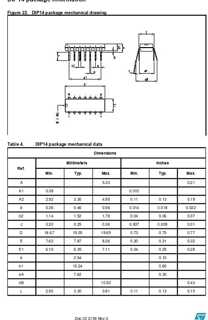
DIP14 package information
Figure 22. DIP14 package mechanical drawing
Table 4. DIP14 package mechanical data
Dimensions
LM139, LM239, LM339 Package information
6.2
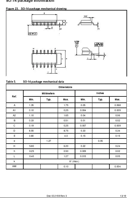
SO-14 package information
Figure 23. SO-14 package mechanical drawing
Table 5. SO-14 package mechanical data
Dimensions
Package information LM139, LM239, LM339
6.3
QFN16 3x3 package information
Figure 24. QFN16 3x3 package mechanical drawing
14/19 Doc ID 2159 Rev 3
LM139, LM239, LM339 Package information
Table 6. QFN16 3x3 mm package mechanical data (pitch 0.5 mm)
Dimensions
Millimeters Typ.
Figure 25. QFN16 3x3 footprint recommendation
Doc ID 2159 Rev 3 15/19
Package information LM139, LM239, LM339
6.4
TSSOP14 package information
Figure 26. TSSOP14 package mechanical drawing
Table 7.
Ref.
TSSOP14 package mechanical data
Dimensions
LM139, LM239, LM339 Ordering information
Temperature
range Package Packing
Revision history LM139, LM239, LM339
8
Revision history
Table 9.
Date
Document revision history
Revision Changes
Initial release.
Updated document format.
Removed power dissipation from Table 1: Absolute maximum ratings.
Added R values to Table 1. Updated package information in Chapter 6.
Added Table 8: Order codes.
Added pin connections for QFN16 package in Figure 1 on page 2. Added thermal information for QFN16 package in Table 1 on page 3. Added QFN16 package information in Chapter 6.
Added order codes for QFN16 package in Table 8: Order codes. THJA, RTHJC, ESD and TLEAD
01-Mar-2003 1
28-Apr-2009 2
13-Jul-2011 3
18/19 Doc ID 2159 Rev 3
LM139, LM239, LM339
Please Read Carefully:
Information in this document is provided solely in connection with ST products. STMicroelectronics NV and its subsidiaries ("ST") reserve the right to make changes, corrections, modifications or improvements, to this document, and the products and services described herein at any time, without notice.
All ST products are sold pursuant to ST's terms and conditions of sale.
Purchasers are solely responsible for the choice, selection and use of the ST products and services described herein, and ST assumes no liability whatsoever relating to the choice, selection or use of the ST products and services described herein.
No license, express or implied, by estoppel or otherwise, to any intellectual property rights is granted under this document. If any part of this document refers to any third party products or services it shall not be deemed a license grant by ST for the use of such third party products or services, or any intellectual property contained therein or considered as a warranty covering the use in any manner whatsoever of such third party products or services or any intellectual property contained therein.
UNLESS OTHERWISE SET FORTH IN ST'S TERMS AND CONDITIONS OF SALE ST DISCLAIMS ANY EXPRESS OR IMPLIED WARRANTY WITH RESPECT TO THE USE AND/OR SALE OF ST PRODUCTS INCLUDING WITHOUT LIMITATION IMPLIED WARRANTIES OF MERCHANTABILITY, FITNESS FOR A PARTICULAR PURPOSE (AND THEIR EQUIVALENTS UNDER THE LAWS OF ANY JURISDICTION), OR INFRINGEMENT OF ANY PATENT, COPYRIGHT OR OTHER INTELLECTUAL PROPERTY RIGHT.
UNLESS EXPRESSLY APPROVED IN WRITING BY AN AUTHORIZED ST REPRESENTATIVE, ST PRODUCTS ARE NOT RECOMMENDED, AUTHORIZED OR WARRANTED FOR USE IN MILITARY, AIR CRAFT, SPACE, LIFE SAVING, OR LIFE SUSTAINING APPLICATIONS, NOR IN PRODUCTS OR SYSTEMS WHERE FAILURE OR MALFUNCTION MAY RESULT IN PERSONAL INJURY, DEATH, OR SEVERE PROPERTY OR ENVIRONMENTAL DAMAGE. ST PRODUCTS WHICH ARE NOT SPECIFIED AS "AUTOMOTIVE GRADE" MAY ONLY BE USED IN AUTOMOTIVE APPLICATIONS AT USER'S OWN RISK.
Resale of ST products with provisions different from the statements and/or technical features set forth in this document shall immediately void any warranty granted by ST for the ST product or service described herein and shall not create or extend in any manner whatsoever, any liability of ST.
ST and the ST logo are trademarks or registered trademarks of ST in various countries.
Information in this document supersedes and replaces all information previously supplied.
The ST logo is a registered trademark of STMicroelectronics. All other names are the property of their respective owners.
© 2011 STMicroelectronics - All rights reserved
STMicroelectronics group of companies
Australia - Belgium - Brazil - Canada - China - Czech Republic - Finland - France - Germany - Hong Kong - India - Israel - Italy - Japan - Malaysia - Malta - Morocco - Philippines - Singapore - Spain - Sweden - Switzerland - United Kingdom - United States of America
www.st.com
Doc ID 2159 Rev 3 19/19
LCD-016M002B
Vishay
16 x 2 Character LCD
FEATURES
•
5 x 8 dots with cursor• Built-in controller (KS 0066 or Equivalent)
•
+ 5V power supply (Also available for + 3V)• 1/16 duty cycle
•
B/L to be driven by pin 1, pin 2 or pin 15, pin 16 or A.K (LED)•
N.V. optional for + 3V power supplyABSOLUTE MAXIMUM RATING MECHANICAL DATA
ITEM
Module Dimension
Viewing Area
Dot Size
Character Size
STANDARD VALUE
80.0 x 36.0
Input Voltage
VDD-VSS
VI
V
V
NOTE: VSS = 0 Volt, VDD = 5.0 Volt
ELECTRICAL SPECIFICATIONS
ITEM SYMBOL CONDITION
Input Voltage VDD
Supply Current IDD
Recommended LC Driving
Voltage for Normal Temp.
Version Module
VDD - V0
LED Forward Voltage
LED Forward Current
VF
STANDARD VALUE
TYP.
DISPLAY CHARACTER ADDRESS CODE:
Display Position
DD RAM Address
Document Number: 37217 Revision 01-Oct-02
For Technical Questions, Contact: [email protected] www.vishay.com 31
LCD-016M002B
Vishay
PIN NUMBER
1
DIMENSIONS in millimeters
16 x 2 Character LCD
Contrast Adjustment
H/L Register Select Signal
H/L Read/Write Signal
HL Enable Signal
+ 4.2V for LED/Negative Voltage Output
Power Supply for B/L (OV)
3.55
www.vishay.com 32
For Technical Questions, Contact: [email protected] Document Number: 37217 Revision 01-Oct-02
0