LabVIEW Simulation for Electroplating Process of
Plated-Through Hole (PTH) in Multilayer Printed Circuit Board
(PCB)
M Arifin1,2*, A B K Atmaja1, and V Octowinandi1,2
1
Department of Electrical Engineering, Politeknik Negeri Batam, 29461 Batam, Indonesia
2
Teaching Factory Manufacturing of Electronics, Politeknik Negeri Batam, 29461 Batam, Indonesia
*E-mail: [email protected]
Abstract. Plated-through hole (PTH) is important part which connect between one layer and other layers in printed circuit board (PCB) multilayer. PTH is commonly made by electroplating process with copper as based conductive material. This research objective to develop the electroplating process in which mass of copper generated using LabVIEW which is used together with Faraday’s law of electrolysis. The results described how to work the electrolysis during electroplating process and the copper mass that adhere in hole and surface multilayer PCB. The results was displayed in LabVIEW interface. On the other hand, experiment of electroplating process is also conducted to form PTH and to determine mass of copper in PCB multilayer. The results showed that PTH was successfully formed in PCB multilayer with electroplating process. The copper mass adhered in multilayer PCB using LabVIEW simulation is not much different with mass of copper experimentally.
1.Introduction
Electroplating is one of the hardest surface adjustment technologies for pre-treatment product. Besides used in electrochemical impedance of lithium battery [1], electrochemical reaction and electric current are applied in this electroplating for making metal coatings. The coating materials frequently used in electroplating are silver, gold, tin, zinc, cadmium, copper, nickel, chromium, and so on [2]. Electroplating is widely used in electronics, aerospace, automotive [3], microelectronic mechanic system (MEMS) technology [4,5,6] and engineering industries. This electroplating has many advantages such as corrosion prevention, aesthetic finishes, coating component [3], lower resistivity, better anti-electromigration ability, and higher thermal exchange rate [7].
(1)
LabVIEW programs are also called virtual instruments. A LabVIEW virtual instrument consists of a front panel, a block diagram, and a connector pane. A front panel is considered as a user interface. In front panel, the user can insert the inputs (sliders, knobs, values entered from the keyboard, push buttons, selector switches) and the outputs (indicators, LEDs, graphs, strip charts, sounds) [13].
A block diagram is considered as a LabVIEW program. Block diagrams integrate terminals, subVIs, functions, constants, structures, and wires, which transfer data among other block diagram objects. Furthermore, a connector panel is a set of terminals on the icon that corresponds to the controls and indicators of a VI, similar to the parameter list of a function call in text-based programming languages [13]. In this research, LabVIEW is applied together with Faraday’s law of electrolysis as in equation (1) [3].
Where m, A, n, I, t, and 96500 are mass of deposited material (gram), atomic weight of deposited
material, valency of deposited material, applied current (Ampere), time (s), and Faraday’s constant
(Coloumb/gram), respectively [3].
3.Experimental procedure
The mass value of copper which it adheres on printed circuit board (PCB) and plated-through hole (PTH) surface is also determined with the experiment. The experiment was conducted through some steps such as PCB design, preparing material, pressing the FR-4 material, drilling, brushing, cleaning, immersing in the conductive carbon, drying, electroplating process, cleaning, drying, and measurement of copper mass.
The prepared material was FR-4 PCB material, distilled water, conductive carbon (black hole solution), and copper (II) sulfate pentahydrate (CuSO4.5H2O, meltex). The first step created a stack
from 3 FR-4 PCB materials with glue and pressing to make four layers of PCB. The pressing process was conducted at 12 bar with temperature 170 oC for 30 minutes. The second step was the drilling process which it works following the PCB design. The PCB design was created using Altium (PCB design software). The third step was brushing and cleaning. The distilled water was used during brushing and cleaning. The fourth step is immersing the PCB surface in the conductive carbon solution (black hole solution) for 5 minutes and drying at 80 oC for 10 minutes. The fifth step is the electroplating process. Before the electroplating process is running, the multilayer PCB was weighed with the scale (Kern FCB bench scale). The electroplating process was conducted for 3 similar PCB, but the applied current for each PCB was different in which the applied current was 15 A, 20 A, and 25 A. Each electroplating process needed 45 minutes. Cleaning and drying of PCB was done after the electroplating process is finished. The last step is measurement of copper mass adhering on PCB and PTH surface.
4.Results and discussion
LabVIEW simulation was used to show how to work electrochemically the electroplating process. It simulated the movement of copper ion in copper(II) sulfate (CuSO4) solution when the electrodes was
(a)
(b)
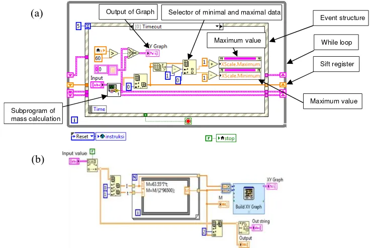
LabVIEW interface displays the table of input data (current, time, copper mass), the simulation of copper ionic movement, and the graph of calculation results. The graph exhibits the relation of applied current and the copper mass. The front panel also displays other parameters such as atomic weight of deposited material, valency of deposited material, and button for play and stop as shown in figure 1.
Figure 1. Interface of LabVIEW virtual instrument for electroplating simulation.
LabVIEW software utilizes the graphical program language that it is placed in the diagram block. The program receives the input data from the front panel such as parameter data, play button, stop button, etc. All program for electroplating simulation and calculation of copper mass is placed in the diagram block as shown in figure 2.
Figure 2. (a) Block diagram of LabVIEW virtual instrument and (b) subprogram of copper mass
calculation during simulation of electroplating process.
Event structure
While loop
Sift register Maximum value
Maximum value Output of Graph Selector of minimal and maximal data
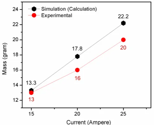
The calculation results of copper atomic mass adhering on the PCB and PTH surface using the equation (1) are 13.3 gram, 17.8 gram, and 22.2 gram for the applied current 15 A, 20 A, and 25 A, respectively. Besides calculation, the copper mass is also obtained from experiment in which it is obtained from difference between the PCB mass before and after the electroplating process. PCB before and after the electroplating is shown in figure 3.
(a) (b)
Figure 3. Multilayer PCB (a) before and (b) after the electroplating process.
The calculation results are slightly different with the experiment results. The experiment results showed that the copper masses on PCB and PTH surface are 13 gram, 16 gram, and 20 gram for the applied current 15 A, 20 A, and 25 A, respectively. There are slightly different of copper mass between calculation results and experiment results as shown in figure 4. The different results of copper mass are possibly caused by impurity of CuSO4 solution and the current difference in amperemeter
and reality.
Figure 4. The comparison between the calculation and experiment results.
5.Conclusion
In this study, the simulation of electroplating process in multilayer printed circuit board (PCB) was successfully created by LabVIEW software. The calculation results of copper mass adhering on PTH and PCB surface are 13.3 g, 17.8 g, and 22.2 g with the applied current 15 A, 20 A, and 25 A,
respectively. Furthermore, the experiment results exhibit that the copper masses are 13 g, 16 g, and 20 g for the applied current 15 A, 20 A, and 25 A, respectively.
Acknowledgments
The authors thank to the Young Lecturer Research Fund Program 2017 from Politeknik Negeri Batam. The authors also thank to Teaching Factory Manufacturing of Electronics (TFME) from Politeknik Negeri Batam that it allowed to use all equipment especially in PCB manufacturing equipment.
References
[1] Arifin M, Rus Y B, Aimon A H, Iskandar F, Winata T, Abdullah M and Khairurrijal K 2017 Mater. Res. Express 4 034005
[2] Selhi A and Nikhil S 2014 Proc. Int. and All India Manufacturing Technology, Design and Research Conf. (Assam: Indian Institute of Technology Guwahti) p 439-1
[3] Masuku E S, Mileham A R, Hardisty H, Bramley A N, Johal C and Detassis P 2002 CIRP Ann Manuf Technol 51 168
[4] Oh S H, Lee K-C, Chun J and Lee M K S S 2001 J. Micromech. Microeng. 11 221 [5] Sadler D J, Gupta S and Ahn C H 2001 IEEE Trans. Magn. 37 2897
[6] Lin M-T, Tong C-J and Chiang C-H 2006 DTIP of MEMS and MOEMS Stresa [7] Chen Y, Li X, Chen S Q and Zhang H 2008 ASME Proceedings 619
[8] Hu C-C and Wu C-M 2003 Surf. Coat. Technol. 176 75
[9] Seah C H, Mridha S and Chan L H 1999 J. Mater. Process. Technol. 89 432
[10] The W H, Koh L T, Chen S M, Xie J, Li C Y and Foo P D 2001 Microelectronics J. 32 597 [11] Khandpur R S 2006 Printed Circuit Board: Design, Fabrication, and Assembly (New Delhi:
McGraw-Hill) p 313
[12] Lin G-Y, Yan J-J, Yen M-Y, Dow W-P and Huang S-M 2013 J. Electrochem. Soc 160 D3028 [13] Boubaker O 2011 Proc. Int. Conf. on Frontiers in Education: Computer Science and Computer