Graphene: Fundamental research and potential applications
Yujia Zhong, Zhen Zhen, Hongwei Zhu
⇑State Key Laboratory of New Ceramics and Fine Processing, School of Materials Science and Engineering, and Center for Nano and Micro Mechanics, Tsinghua University, Beijing 100084, China
a r t i c l e
i n f o
Article history: Received 11 May 2017 Revised 20 June 2017 Accepted 20 June 2017 Available online 22 June 2017
Keywords: Graphene
Two-dimensional materials
a b s t r a c t
Graphene is a representative two-dimensional (2D) material and has been receiving considerable interest from both academia and industry. In this review, we recollect the latest development in the synthesis, struc-tural analysis, characteristics, and possible applications of graphene materials. The discussion helps researchers to better understand the properties of graphene and design novel graphene-based applications. Ó2017 Elsevier B.V. All rights reserved.
Contents
Introduction. . . 20
Synthesis and transfer . . . 21
Solid phase method. . . 21
Solution phase method . . . 21
Preparation of graphene nanoribbons . . . 22
Chemical vapor deposition . . . 22
Transfer . . . 22
Structure and morphology . . . 23
Properties. . . 24
Electrical properties . . . 24
Optical properties . . . 25
Thermal properties . . . 25
Mechanical properties. . . 25
Chemical modification . . . 25
Applications . . . 26
Electrical applications . . . 26
Mechanical applications . . . 27
Mass transport. . . 28
Substrates . . . 28
Perspectives . . . 29
Conclusions . . . 30
Acknowledgments . . . 30
References . . . 30
Introduction
Graphene is the first synthetic two-dimensional (2D) atomic crystal. It has attracted immense attention because of its excellent
properties, including stiffness, strength, elasticity, high thermal conductivity, extremely high electron mobility, and tunable band gap. Being such a fascinating all-in-one material, graphene can replace other materials in many applications and bring about
http://dx.doi.org/10.1016/j.flatc.2017.06.008
2452-2627/Ó2017 Elsevier B.V. All rights reserved.
⇑Corresponding author.
E-mail address:[email protected](H. Zhu).
Contents lists available atScienceDirect
FlatChem
technological breakthroughs. Graphene has been investigated the-oretically since the 1940s[1]. However, its studies mostly focused on theoretical calculations. It was only until 2004 [2], through exfoliating highly oriented pyrolytic graphite[3], that graphene was first prepared in the laboratory. This experimental success stimulated research in 2D materials. From 2004 till now, more than one hundred research articles on graphene have been published in
ScienceandNature. In this review, we recollect the latest develop-ment in the synthesis, structural analysis, characteristics, and potential applications of graphene materials, to address the contin-ued developments and challenges with a wide scope of interest, highlighting fundamental understanding of the synthesis and characterization procedures, future outlook, as well as an in-depth discussion of high-end application areas. The discussion helps researchers to better understand the properties of graphene and design novel graphene-based applications.
Synthesis and transfer
The synthesis of graphene is currently still a key concern in gra-phene research. Although several methods, with varying cost and yield, are available, they still pose restraints on the studies and applications of graphene.
Solid phase method
The synthetic methods can be classified by the phase of carbon source and the synthetic environment (Fig. 1). Solid phase methods include mechanical exfoliation[3]and synthesis on SiC[4]. Gra-phene can be acquired by mechanically exfoliating highly oriented pyrolytic graphite with tape (Fig. 1A). The resulting graphene has excellent quality, but the yield is low and the cost is high[3,5].
Alternatively, graphene can also be epitaxially grown on single crystal SiC by vacuum graphitization[4](Fig. 1B). The number of epitaxial graphene layers can be controlled, and the quality of such graphene is good. However, the carrier scattering at epitaxial gra-phene on SiC is induced by geometry. Thus the size of electrically uniform domains is limited[6]. This method allows preparing gra-phene of larger sample size, but it is costly because it requires high reaction temperature and the very expensive SiC wafers. In addi-tion, the prepared graphene is inferior to the mechanical exfoliated graphene in quality and crystallite size.
Solution phase method
The oxidation–reduction reaction is a widely used solution phase method to synthesize graphene-derived materials, such as graphene oxide (GO). This method has low cost and gives high yield, but the product has inferior quality. The GO fabricated via solvent casting can completely exfoliate in water (Fig. 1D) to produce sus-pensions containing almost entirely individual GO sheets[7,8].
The suspension can be deposited as a thin film on many surfaces, and the film can then be reduced[5]. Subjecting GO to reducing agent under certain condition gives reduced GO (rGO). Alternatively, GO can be reduced by heating in an inert atmo-sphere. Catalysts induce GO reduction upon illumination or annealing at high temperatures. And it is environmentally friendly to reduce GO by applying voltage[9]. The use of heated atomic force microscope (AFM) tip [10], laser beam[11] and pulses of microwaves[12]allows reducing GO with precision (Fig. 1E). Ther-mochemical nanolithography with heated AFM tip can pattern the nanoscale rGO without tip wear or sample tearing. The width of the rGO patterns can be controlled between 12 nm and 20
l
m [10]. Similarly, reduction through laser irradiation can also pattern rGO[11]. Both methods are reliable, flexible, clean, and rapid.Solid phase methods
Solution phase methods
Chemical vapor deposition (CVD)
Mechanical exfoliationCNT unzipping Synthesis on SiC
Liquid-phase exfoliation
Reduction of GO Monomer assembly
SiC
Graphene
GO
Laser Hot AFM tip
Graphene
Cu Ni
CH4
C H
CH4
C H
Graphene Graphene
A
B
C
D
E
F
G H
Beside the oxidation–reduction method, a non-chemical solution-phase exfoliation of graphite in organic solvents is devel-oped[13,14]. Few-layer graphene can be obtained by dispersion and exfoliation of graphite in N-methyl-pyrrolidone (NMP), N,N-Dimethylacetamide (DMA),
c
-butyrolactone (GBL) and 1,3-dimethyl-2-imidazolidinone (DMEU).Preparation of graphene nanoribbons
Graphene is a 2D zero band gap semimetal. Therefore, its band gap must be opened up before it can replace Si and be used in elec-tronics. Because quantum confinement and edge effects can intro-duce band gaps (Eg) (1/wa, wherewis the width and
a
is nearunity) in graphene nanoribbons (GNRs), the GNRs whose width is less than 10 nm exhibit semiconductor nature and have substantial band gap (Eg> 0.3 eV)[15]. Narrow GNRs can be produced through chemical sonication. For example, sonicating the solution of poly (m-phenylenevinylene-co-2,5-dioctoxy-p- phenylenevinylene) (PmPV) in 1,2-dichloroethane (DCE) gives a suspension of exfoli-ated graphite, which is further centrifuged to obtain the GNRs[15]. Lithographic patterning[16]of graphene film is a conventional technique to acquire GNRs. GNRs prepared by lithographic pattern-ing are wide, but limited in width and smoothness. Carbon nan-otube (CNT) can be regarded as a GNR rolled up into a seamless tube. As a result, it is logical to produce GNRs by unzipping CNTs. CNTs partly embedded in a polymer film can produce GNRs through plasma etching (Fig. 1C). If the starting CNTs have small diameter and certain chirality, the obtained GNRs may have well-defined widths and edges. Selecting the CNTs and modifying the plasma etching time will manipulate the number of graphene lay-ers and affect the yield. This method allows large scale production of narrow (<10 nm) GNRs that have well-aligned morphology, con-trolled structures, and band gaps suitable for semiconductivity [17]. Annett and Cross heated the exfoliated single layer graphene (SLG) with Si substrate to 150°C for 13 days. The thermal activa-tion lead to the spontaneous sliding, tearing and peeling of gra-phene and further formed GNRs [18]. Solution-based oxidation can cut multi-walled CNTs lengthwise to yield ribbon structures, and subsequent chemical reduction can produce GNRs and restore the electrical conductivity. Although this method is expected to produce GNRs with zigzag edge, in practice it does not generate the desired structure[19].
A bottom-up approach assembles precursor monomers into lin-ear polyphenylenes and then makes atomically precise GNRs by cyclodehydrogenation (Fig. 1F)[20,21]. Straight GNRs with arm-chair edges are made from bianthryl monomers, and Chevron-type GNRs with armchair edges are made from tetraphenyl–triphe nylene monomers[20]. However, two problems exist,i.e., polymer-ization can occurviaaryl-aryl coupling along the armchair direc-tion, and cyclodehydrogenation of phenyl subgroups does not always ensure pure zigzag edges. Zigzag-edged GNRs can be syn-thesized by the polymerization of U-shaped dibenzo anthracene monomer with halogen functions at both ends and dimethyl-biphenyl in the interior, and then subsequent cyclization [21]. Thus, the topology, edge, and width of GNRs can be controlled by using different precursors in polymerization and cyclization. Recently, high quality GNRs are acquired through chemical vapor deposition. h-BN substrates are used as the templates. The in-plane epitaxy of GNRs ensures smooth edges with controllable width[22].
Chemical vapor deposition
Electronic applications require graphene of high quality and large area, which is often not synthetically available from mechan-ical exfoliation or solution methods. Chemmechan-ical vapor deposition
(CVD), of CH4 on catalyst substrates can render large monolayer or bilayer graphene[23,24]. A typical CVD setup is illustrated in Fig. 1G. Since gaseous carbon source limits the graphene synthesis with different source materials, many solid carbon sources, includ-ing sucrose and polymethyl methacrylate (PMMA)[25], have been exploited to grow large pristine or doped graphene with control-lable thickness on Cu or Ni substrates at 800–1000°C [25]. The main advantages of CVD include lower temperature growth and flexible choices of raw materials. Large area and good quality gra-phene is easy to produce by CVD. However, it always costs several hours to acquire a continuous graphene film, which means low yields in industrial production. Both CVD growth and subsequent transfer procedures induce defects in graphene. Growth near 1000°C leads to high energy costs. The subsequent transfer con-sumes metal substrate and produces defects in graphene film. The cost of CVD is higher than that liquid-phase methods.
The mechanism of graphene growth in CVD (Fig. 1H) depends on the substrate. Carbon is dissolved in Ni at high temperatures. The dissolved carbons segregate and precipitate to form graphene during the cooling process with appropriate cooling rates[26,27]. In contrast, carbon has negligible solubility in Cu and deposits directly on the Cu surface[23]. Wrinkle-free single crystal single layer graphene (SLG) can be synthesized on the reusable hydrogen-terminated Ge substrate [28]. The CVD parameters, including C/H ratio, substrate quality, temperature, and pressure, can all influence the graphene quality. Oxygen on the Cu surface can passivate Cu and hence decrease graphene nucleus. Besides, the dehydrogenation effect of oxygen alters the growth behavior of graphene[29]. The presence of oxygen makes it easier for carbon to attach on graphene edge, and thus accelerates graphene growth. This mechanism is diffusion-limited, which corresponds to the shape of the dendritic domain. Without oxygen, the growth kinet-ics is limited by edge attachment and the morphology of the gra-phene domain is compact.
Beside graphene sheets, three dimensional (3D) graphene archi-tecture carrying periodic nanopores is also of great interest. As a kind of microporous crystalline aluminosilicate, zeolite is an ideal a template for making 3D graphene architectures. Lanthanum helps form 3D graphene architectures because adding lanthanum ions to zeolite pores reduces the carbonization temperature of ethylene or acetylene. As a result, graphene can be selectively grown inside the zeolite template instead of being deposited on the zeolite surface[30].
Transfer
for patterning. When a patterned layer of Zn is sputtered atop the multilayer graphene, cleaning Zn with aqueous HCl can simultane-ously remove one graphene layer[34].
Structure and morphology
Graphene is a single atomic 2D layer of sp2-bonded carbon packed into a honeycomb lattice. All carbons havesp2 hybridiza-tion and the residual electrons in theporbital form large
p
bond. Ther
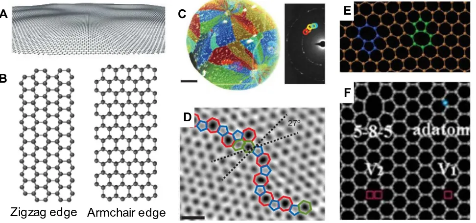
bonds formed by thesp2-bonded carbon make graphene stable and flexible. Theoretical studies demonstrated that thermal fluctuations would destroy the long-range order of 2D lattice. However, graphene with elastic corrugation (Fig. 2A) can with-stand thermal fluctuation through modulating bond length[35]. For bi-layer graphene (BLG), the buckling at the dislocations can completely delocalize the respective residual compressive and ten-sile strains in two graphene layers[36]. The fabrication of SLG that is flat down to the atomic level by deposition on cleaved mica sur-face can help study the impact of ripple on the graphene proper-ties. When graphene is supported on an atomically flat substrate such as mica, its intrinsic ripples would be strongly suppressed by the interfacial interactions[37].The edge of graphene can be typically classified as either zigzag or armchair (Fig. 2B). The zigzag edge GNRs show metal properties, whereas the armchair edge GNRs can be of either metal or semi-conductor nature. The behavior of atoms at the edge of the SLG sheet can be analyzed by comparing the aberration-corrected TEM images with simulation results. The rearrangement of carbon atoms under prolonged irradiation reveals that the zigzag edge configuration is more stable 38. Single atom energy-loss spec-troscopy can also help to get abundant chemical information of carbon atoms at graphene edge[39].
When the orientations of adjacent grains are different, grain boundaries (GBs) are formed (Fig. 2C). The GBs in graphene are formed by integrating islands during the initial growth stage. It is observed in atomic-resolution aberration-corrected annular dark-field scanning transmission electron microscopy (ADF-STEM) imaging that graphene grains are stitched together through
pentagon-heptagon pairs (Fig. 2D)[40]. The location of graphene GBs can be conveniently visualizing in optical microscope through water photolysis, in which the hydroxyl moiety bonds with GBs and oxygen traverses graphene through GBs to form oxide with the Cu substrate[41]. Because the structure of grain boundary is different from the grain structure, the presence of GBs changes the properties of graphene. The defect density and the strength of polycrystalline graphene are determined by the angle of tilt boundaries. Graphene with large-angle tilt boundaries, which have a higher density of defects and can better accommodate strained rings, is much stronger than those with low-angle boundaries. The strength of large-angle tilt boundaries graphene is nearly the same with pristine graphene [42]. AFM nanoindentation results reveal that if the GBs are well stitched, the elastic stiffness and strength of CVD graphene are comparable to those of pristine gra-phene. Hence, well stitched GBs do not impair the mechanical properties of graphene [43]. If the graphene grains overlap but do not covalently join, the GBs would be weak, but the electrical conductance could be higher than that of stitched boundaries. In contrast to overlapped grains, when gaps exist, the conductance of the well stitched grains and the adjoined grains would reduce [44].
The second law of thermodynamics dictates that disorder should appear in crystalline materials. Many properties of materi-als are governed by defects. Defects in graphene can be useful in adjusting the structure and properties of graphene. The first direct evidence for atomic defects in graphene layers was obtained by comparing thein-situHRTEM images of graphene before and after sputtering with simulated results (Fig. 2F)[45]. The movement of dislocations is the key mechanism for understanding the deforma-tion in materials. In layered crystals, the dislocadeforma-tions are restricted to the basal plane. Graphene is a suitable subject to explore the dis-location movement in layered crystals. Warner et al. studied the dislocation movement, interaction, and strain fields in graphene. The dislocations in SLG can be seen as pentagon-heptagon pairs. The edge dislocations lead to C–C bond compression or elongation of ±27%, as well as shear strain and lattice rotations. The disloca-tion pairs (Fig. 2E) affect each other if their distance is less than
F
Armchair edge
Zigzag edge
A
B
C
D
E
Fig. 2.Structure and morphology of graphene. (A) Corrugated graphene[35]. (B) Zigzag edge GNR and armchair edge GNR. (C) Left panel: grains emanated from a few points. Right panel: diffraction pattern taken from a region in the left image. The diffraction pattern reveals that this area is polycrystalline[40]. (D) Atomic-resolution ADF-STEM images of graphene crystals[40]. (E) Dislocation pair in graphene[46]. (F) Four defects types in graphene: an adatom, unrelaxed vacancies (V1and V2) and a 5-8-5
1.5 nm. When the area of the dislocation pairs in graphene is deformed through the electron beam irradiation, the strain field is localized around the core[46]. Basal-plane dislocations in BLG are real line defects confined between the two graphene layers. Since BLG has no stacking-fault energy, the dislocations change the local stacking from AB to AC[36].
Properties
Electrical properties
In graphene, the carbon atoms havesp2hybridization as the
r
state, and the residualporbital electrons form conjugatedp
bond and move freely. Threer
states in one graphene unit cell form the lower valence states, and delocalizedp
andp
⁄ states form thehighest occupied valence states and the lowest unoccupied con-duction band [47]. Graphene is a zero band gap semimetal [47,48] whose conduction band and valence band show conical dispersion and meet in the Dirac point (Fig. 3A)[49]. The linear dis-persion of electron results in an effective massm⁄= 0 at the Dirac point. Considering the interactions between quasiparticles, the Dirac spectrum would reconstruct[50]. The reconstructed Dirac crossing includes one crossing between pure charge bands, another
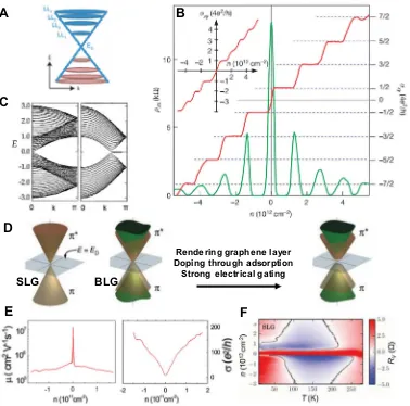
between pure plasmaron bands, as well as a ring-shaped crossing between charge and plasmaron bands[51]. Charge carriers in con-ductors circulate in cyclotron orbits with quantized energies under magnetic field. The quantized energies, which are called Landau levels, are equally spaced in normal metals and 2D electron gases [52]. Song et al. studied the degenerated graphene Landau level and explored the detailed features of the quantum states[53]. Gra-phene appears different with conductors in that its charge carrier velocity is independent of the quantized energies, thus the Landau levels are not equally spaced and include a characteristic zero-energy state (Fig. 3A)[52]. Since electrons in graphene are confined in a 2D film, anomalous quantum Hall effect (QHE) (Fig. 3B) can be observed[49,54–63].
The edge of the graphene determines its magnetic and electronic properties. GNRs with zigzag edges show the half-metallicity with zero band gap and provide a platform to explore spintronics[38]. Furthermore, their magnetic properties are dominated by the exter-nal in-plane homogeneous electric field across their zigzag edges. In contrast, the energy band of narrow armchair GNRs indicates that they are a semiconductor with small band gap (Fig. 3C) [15,17,19–21,64]. Tuning the graphene edges to acquire specific crystallographic orientation can increase magnetic order. The nar-row (5 nm) zigzag GNR is an antiferromagnetic semiconductor,
SLG
BLG
Rendering graphene layer Doping through adsorption
Strong electrical gating
A
C
E
B
D
F
but the wide (>8 nm) zigzag GNR is ferromagnetic with no bandgap [65].
The electrical properties of graphene are also affected by the symmetry of its hexagonal layer structure. Topological currents can be observed in graphene superlattices that have broken inver-sion symmetry[66]. Because of its parabolic dispersion, the bilayer graphene is susceptible to the symmetry breaking induced by the interactions among charge carriers even at zero magnetic fields [67]. When the BLG has Bernal stacking, the band structure consists of
p
,p
⁄states and two lower energy bands through the splitting valley from interlayer coupling. The band gap of the pris-tine Bernal-stacked BLG is zero. The band gap of BLG can also be opened or closed by rendering the individual graphene layer, dop-ing through adsorption[47], or strong electrical gating in dual-gate BLG FETs (Fig. 3D)[68]. The electromechanical properties[69,70] are used to explore the electrical properties. Because graphene has massless Dirac fermions-like band structure and lattice sym-metry, the pseudo-magnetic fields induced by strain can approach 300 T, which offers a method to control the electronic structure of graphene[69].The sheet resistance5 of highly doped graphene reaches 30X/sq. The electron mobility (
l
) can rise up to 2105cm2/(Vs) at electron densities (n) of 21011cm 2in suspended SLG
(Fig. 3E)[71]. The CVD SLG transferred to SiO2substrate[26]shows electron mobility
l
= 3700 cm2/ (Vs) at n= 51012cm 2. The
conductivity
r
=nel
is controlled by both electron mobility and charge density. Compared with Cu, graphene shows higher elec-tron mobility but has much lower charge density. Zhao et al. found that the electronic structure of the individual nitrogen dopant in SLG changed only within a few lattice spacing, and this allows increasing carrier density while conserving graphene quality[72]. Under magnetic field, supercurrent could be observed in encapsu-lated graphene in contact with superconducting electrodes[73]or in a graphene layer contacted by two closely spaced superconduct-ing electrodes[74]. In graphene junction which is contacted by two closely space superconducting electrodes, a finite supercurrent is observed even at zero charge density [74]. In some situations, graphene can show ballistic transport property[75–77]. Ballistic propagation means that scattering only occurs at the quantum bil-liards boundaries, as is observed in the low-temperature transport spectroscopy of SLG or BLG. Epitaxial GNR (40 nm wide) features single-channel room-temperature ballistic conductors with a bal-listic length more than 10l
m [78]. Ju et al. observed ballistic valley-polarized conducting channel with a ballistic length of 400 nm at 4 K[79]. Rutter et al. found that intravalley and interval-ley backscattering was dominated by the in-plane atomic defect, thus the defect influenced the transport properties of graphene [80]. Bandurin et al. demonstrated that electrons in graphene behave like a viscous liquid (Fig. 3F) [81], because in graphene electron-phonon scattering is weak but electron-electron collisions abound. The vicinity resistance is negative over a large range of carrier density and temperature, and the viscosity of electron Fermi liquid in graphene is0.1 m2/s.Optical properties
The optical transmittance (T) and reflectance (R) of graphene are given byT(1 + 2
p
G/c) 2andR0.25p
2a
2T, whereG=e2/4⁄(⁄=h/2
p
,his the Planck constant,eis the electron charge) is the high-frequency conductivity for Dirac fermions in graphene,c is speed of light, anda
=e2/⁄c1/137 is the fine structure constant
that describes the coupling between light and relativistic electrons. Reed et al. reported that the value of effective fine-structure con-stant is
a
= 0.14, which is smaller than the nominala
= 2.2 and suggests that the strength of interaction between quasiparticles is weaker than previously believed [82]. The reflectance ofgraphene is negligible (<0.1%). Though SLG is only one atom thick, its opacity can reach (1 T)
pa
2.3%. The opacity can increaseanother 2.3% for one more graphene layer and is independent of the wavelength of the incident light [83]. The optical behavior results from the confinement and low density of states near the Dirac point in graphene. Thus, optical study can help in studying the graphene band structure. From the infrared spectroscopy of SLG and BLG, Wang et al. found that optical transitions in graphene can be modified through electrical gating[84]. Liu et al. managed the Fermi level by adjusting the drive voltages and made a graphene-based broadband optical modulator that gave tunable response[85]. In normal circumstances, it is hard to control optical fields because photon is neutral, but tuning the carrier density in graphene allows changing the plasmon polaritons and the associ-ated optical fields[86,87].
Thermal properties
Graphene has high thermal conductivity (
j
) value because of the strong bonding of its carbon atoms. The thermal conductivity of a suspended SLG is determined from Raman spectroscopy to bej
5000 W/mK, which exceeds that of diamond and graphite[88]. Suspended graphene has higher
j
than supported SLG, because in the latter phonons can leak across the graphene-support interface and strong interface-scattering is introduced by the contact. Graphene samples grown by thermal decomposition, CVD, and exfoliation have different interactions with the support-ing surfaces. An SLG exfoliated on a SiO2support has higher ther-mal conductivity (about 600 W/mK) than copper[89].Mechanical properties
The mechanical properties of free-standing atomically perfect nanoscale SLG were measured by nanoindentation in an atomic force microscope. The results showed that Young’s modulus is
E= 1.0 TPa and intrinsic stress is
r
int= 130 GPa [90]. However, the mechanical properties of graphene are affected by many fac-tors, such as defects, stitching quality of adjacent boundaries [43], and angle of tilt boundaries[42]. The dynamic mechanical behavior of multi-layer graphene (MLG) in the extreme dynamic condition was observed through supersonic projectile penetration. The MLG deformed into a cone and then formed radial cracks extending along crystal orientations to the outside of the impact area[91]. Superlubricity is important to save energy and enhance device lifetime. Choi et al. demonstrated the anisotropic friction of graphene,i.e., the friction varies with the angle between the rip-ple line of graphene and the force[92]. The friction force between GNRs and Au substrates fell in the range of 100 pN, which meant superlubricity. The friction behavior was studied in ultrahigh vac-uum from the atomically well-defined GNR–Au (1 1 1) contact[93]. Recently, the results of atomistic simulations reproduce the experimental frictional phenomenon of graphene, including layer-dependent friction and transient frictional strengthening on graphene. The simulations reveal that true contact area governing friction on two-dimensional materials. Producing wrinkles on sus-pended graphene can greatly increase the total friction force with-out obvious change in the true contact area[94].Chemical modification
the magnetic moment induced by the adsorption of single hydro-gen atom, hydrohydro-genation could also control the graphene mag-netism at atomic scale[97].
Applications
Electrical applications
Many studies focus on the applications of graphene. Even at the scale of a few benzene rings, the mechanical, chemical and con-ducting properties of graphene can still remain. Thus graphene is suitable in working as molecular-scale electronics[98]. Addition-ally, when the type and density of the carrier in the SLGp-n junc-tion is customized[56], graphene can serve as semiconductor layer in barristor[99], field effect transistor (FET)[44,100–102], as well as integrated circuit[103,104]. Graphene can also work as capaci-tor[11,105–107]and sensor[108,109]. When the carrier densities onn- andp- sides of the single graphenep-njunction are made exactly equal, the electron flow can then focus. Accordingly, gra-phene can be used to produce electronic lens [110]. Inspired by the whispering-gallery mode, Zhao et al. designed resonators for electronic waves by forming circular p-n junctions in graphene [111]. Graphene barristor [99] is a triode device with a
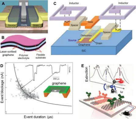
gate-controlled Schottky barrier that has an on/off ratio of 105. Wu et al. reported a top-gate CVD-graphene transistor on diamond-like carbon (Fig. 4A). This transistor has short gate length to help increase the performance, and its performance is relatively stable with the change of temperature[101]. Based on vertical graphene heterostructure, a field-effect tunneling transistor device was pro-posed[102]. The device exploits the low density of states in gra-phene, thus a small change ofVgcan lead to a greater increase inEf. Graphene is useful not only in electronic devices, but also in photonics and optoelectronics that combine the optical and elec-tronic properties[112]. In most optoelectronic devices, graphene functions as a transparent conductor for its low sheet resistance and high transparency. Graphene based transparent conducting films can be used as window electrodes and hole transport layers in inorganic[113], organic[114,115]and dye-sensitized solar cells [116]. Graphene has a work function of 4.5 eV, which is similar to indium tin oxide (ITO). The flexibility of graphene makes it suitable in flexible devices. In light-emitting devices [117] and touch screens[118], there are many attempts to use graphene to replace ITO. Graphene can absorb a wide-spectrum light from ultraviolet to terahertz. Therefore, a graphene photodetector is expected to real-ize broader spectral detection. For example, Xia et al. have reported an ultrahigh-bandwidth photodetector based on few-layer
C
D
A
B
E
graphene[119]. Furthermore, graphene has a high carrier mobility, which may also bring an ultrafast response.
Laser reduction graphene has large surface area and fine mechanical and electrical properties. Therefore, electrochemical capacitors with graphene electrode (Fig. 4B) exhibit high energy density, high power density, and remarkable cycle stability[11]. Double-layer capacitors (DLCs) with electrodes of vertically oriented graphene nanosheets have low electronic resistance, desirable resistor-capacitor (RC) time constants, and excellent AC line-filtering performance. Using graphene nanosheets to introduce more exposed edge planes can increase the charge storage of the capacitor[92]. The a-MEGO is prepared from microwave exfoliated GO (MEGO) upon KOH activation and has a continuous 3D network with nanoscale pores. Its structure helps the supercapacitors over-come the limit of low energy storage density and high series resis-tance[106]. Capillary compression of graphene gel films in liquid electrolyte can produce continuous ion transport network[107]. Porous graphene/polyaniline (PANI) nanocomposites is also suit-able for supercapacitor applications[120]. Gabor et al. used local laser to excite FET and observed the resistance change with varying top-gate and bottom-gate voltages[121]. They demonstrated that the intrinsic photoresponse in graphene was nonlocal hot carrier transport. Graphene was also used to fabricate integrated circuit (Fig. 4C) in which graphene FET and inductors were monolithically integrated on a single SiC wafer[103]. Lenvendorf et al. proposed a patterned regrowth method to synthesize lateral junctions between graphene andh-BN or between pristine and doped gra-phene[104]. This method makes it possible to fabricate integrated circuitry.
The in-plane conductivity of graphene can reflect the atomic-scale information of its opposing interfaces. This is because the gra-phene trans-electrode membrane (Fig. 4D) attracts cations and anions from ionic solution to its opposing surfaces. The interaction between the ions and the membrane is mediated by graphene and electric fields. Since the in-plane electronic conductance is sensitive to the interfacial environment, the trans-electrode can serve as a detector. For example, during DNA translocation, the trans-electrode can be used to identify the type of DNA through different nanopores current blockades versus blockade duration (Fig. 4D) [108]. A mid-infrared plasmonic biosensor (Fig. 4E) is designed by exploiting the electro-optical properties of graphene as follows. Protein molecule is adsorbed on GNRs, and the interaction of the molecule with light is increased by GNRs under infrared beam. The molecule is identified by the dips of the plasmon resonance spectral shift, which reflects the vibration bands of proteins[96]. The nanocomposites of graphene and Silly Putty display electrome-chanical behavior[122]. The resistivity of nanocomposites changes with strain. The gauge factors of the nanocomposites electrome-chanical sensors exceed 500.
Mechanical applications
The GO structure also shows excellent mechanical properties. GO nanosheets can arrange as interlocking tile, which results in good flexibility and stiffness (Fig. 5A)[8]. Bunch et al. made an electromechanical resonator by laying graphene sheet over a trench in silicon oxide. The vibration of this resonator is driven by optical or electrical signal, and the device can detect ultralow mass change and ultrasensitive force (Fig. 5B) [123]. Berman et al. wrapped graphene around nanodiamonds to form nanoscrolls and used them to decrease the friction between nanodiamonds and diamond-like carbon (DLC) (Fig. 5C)[124]. The wrapping of gra-phene was influenced by the humidity of air.
Xin et al.[125]utilized the mechanical properties of graphene and reported graphene fibers in which large graphene sheets direc-tionally aligned with some mixture of small graphene sheets
(Fig. 5D). These fibers were fabricated through thermally annealing the aligned GO fibers, and they combine high thermal and electri-cal conductivity with excellent mechanielectri-cal strength. The property of the fibers was affected by the ratio of small and large graphene sheets and the annealing temperature. Liu et al.[127] stack and shear scroll graphene/polycarbonate composites. The scrolled fiber promises strength, elongation and conductivity.
Seeing that graphene is comparable to paper in the ratio between in-plane stiffness and out-of-plane bending stiffness, Blees et al. applied ideas from kirigami to graphene sheets and pat-terned graphene through optical lithography[126]. For instance, the graphene in-plane kirigami springs can be stretched by 240% without a notable change of conductance (Fig. 5E).
Besides, graphene is also used as a filter in nanocomposites. Graphene and polymer can be mechanically mixed. For example, adding 0.7 wt% GO in poly(vinyl alcohol) (PVA) leads to 76% increase in tensile strength and 62% improvement in Yong’s modu-lus[128]. Dispersion of graphene in polymer matrix and the inter-action between graphene filter and polymer matrix are the key concerns of graphene-polymer nanocomposites. Some graphene nanocomposites are prepared through nucleation and growth, and graphene functions as the substrate for polymer nucleation.
Small
Fig. 5. Mechanical applications of graphene. (A) The schematic draw of the uniaxial and bend test of interlocking-tile GO sheets[8]. (B) Suspended graphene resonator
Mass transport
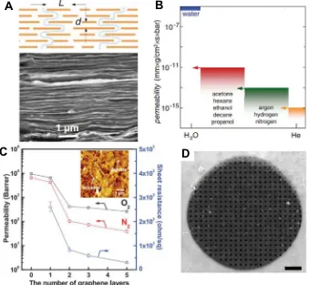
Since graphene with perfect quality shows impermeability, it is used to seal the water on mica to observe the growing mechanism of water adlayers [129]. Selective permeability is also possible when the structure or chemical property of graphene is adjusted. GO membranes are the first use case of such kind of selective per-meability. Submicron-thick GO membranes, which are even imper-meable to helium, allow unimpeded permeation of water through the capillaries formed by closely spaced GO sheets (Fig. 6A and B) [130]. Ultrathin GO membranes prepared by facile filtration[131] and spin-coating[132]can preferentially sieve gas mixtures. The filtration GO membranes can separate CO2and H2because it is per-meable only to the gas molecule whose kinetic diameter is small than the lamellar spacing of GO. When the thickness of the mem-brane is enhanced, the mechanism of permeation will change,i.e., the molecule will penetrate the membrane through the defects and cracks of GO. In addition, the selectivity of spin-coating GO mem-brane can be controlled via different stacking methods. According to Joshi [133], the velocity of small ions that permeate through GO membrane is much quicker than the velocity of diffusion, pre-sumably because the graphene capillaries exert high pressure on small ions. Kim et al.[132]studied the selectivity and permeability of graphene/ Poly(1-methylsilyl-1-propyne) (PTMSP) membrane and found that the existence of SLG does not influence the gas per-meability of PTMSP membrane (Fig. 6C). Celebi et al. physically punched pores on bilayer graphene by focused ion beam[134]. The drilled pores (Fig. 6D) were between 10 nm and 1
l
m in diam-eter and enabled H2/CO2selectivity and ultimate permeation.Substrates
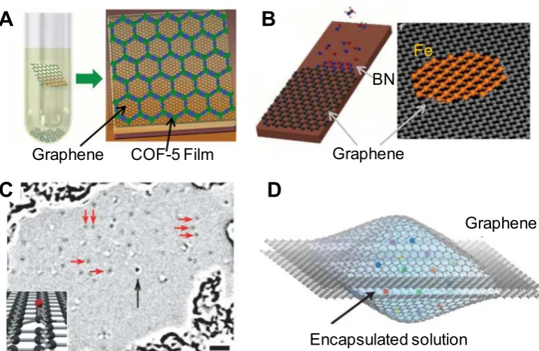
Graphene also helps in preparing and growing other materials. Using graphene as the substrate in GaN growth resolves the diffi-culty in transferring GaN. Since GaN cannot be grown directly on pristine graphene, ZnO nanowall was used as an interlayer between graphene and GaN. This graphene/ZnO/GaN combination shows excellent optical characteristics and is used to produce photoelectri-cal device such as LEDs [135]. Solvothermal condensation of 1,4- phenylenebis (boronic acid) and 2,3,6,7,10,11- hexahydroxyt-riphenylene in the presence of substrate-supported graphene in a vessel generates a covalent organic frameworks (COF-5) film on the graphene surface and precipitated powders. Graphene helps improve the crystallinity of the COF-5 film (Fig. 7A)[136]. The substrate-epilayer gap accommodate a monolayer of graphene. Gra-phene is thin enough to guide the epitaxial orientation. Thus, gra-phene assists remote homoepitaxy. The epilayer is easy to release and transfer. This character overcomes lattice-matching limitation in epitaxy[137]. Xu et al.[138]developed a facile method to pro-duce hierarchical nanocomposites of PANI nanowire arrays on GO sheets. Here GO functions as a component in the nanocomposite and the substrate for PANI nanowires nucleation and growth.
Monolayer crystalline h-BN can be grown from fresh edges of SLG (Fig. 7B). The growth mechanism is coherence, thus the h-BN lattice orientation only depends on the orientation of graphene [139]. In the transfer process of graphene, etching Cu in FeCl3 solu-tion leaves some remnant Fe atoms. Zhao et al.[140]found that these Fe atoms form free-standing single-atom-thick membranes suspended in graphene pores (Fig. 7B). These Fe atom membranes
A
B
C
D
are produced by electron-beam irradiation with the help of dan-gling bonds, and they gradually decompose under electron-beam irradiation.
Moreover, graphene helps visualize ultra-low-contrast objects in TEM, thus clean SLG membrane is a good substrate to observe hydrogen and carbon atoms (Fig. 7C)[141]. Liquid cell wrapped by graphene (Fig. 7D) is employed to explore the mechanism of colloidal platinum nanocrystal growth[142]. Similarly, graphene nanocapillaries help to examine water confined in nanocapillaries (square ice) [143]. Graphene can be the substrate of polymer superstructure to help capture the transmission dynamic by ultra-fast low-energy electron diffraction[144].
Perspectives
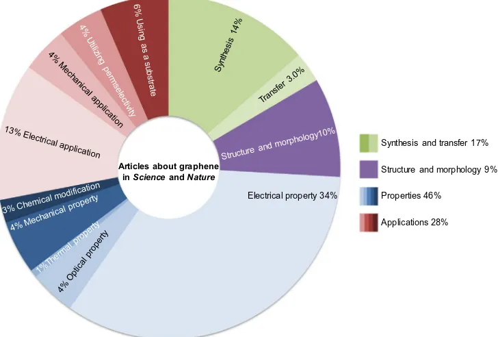
With all fascinating properties that a theoretical graphene material could have, the application of graphene is considered as the gate to reach some advanced technology such as biological engineering, advanced electronics, high efficiency energy genera-tion and storage, flexible wearable sensors, portable water treat-ment, and superior structural material. This trend is consistence with the data collected of the latest publications about graphene materials. According to the pie chart, electrical property and appli-cations are the most famous spots of graphene research which summed up to 47% of total publications.
In recent years, substantial efforts have been put into developing electrical applications of graphene thin films, but the progresses are mostly still in the research prototyping stage. One of the main rea-sons lays to the difficulty in obtaining high quality graphene with an affordable cost. Synthesis of inch sized single crystal graphene with ultrahigh mobility requires extreme conditions and demand-ing trials which only can be achieved in countable research labs in the world. On the other hand, most graphene thin film available on the market has many defects with a resistance around hundreds
ohms which is not suitable for application in high performance electrical devices. Taking touch screen as an example, graphene film is capable to make qualified pressure sensor for touch screen. How-ever, such product is simply offered an alternative for the existing ITO touch screen with few advantages in performance and cost. Similar situation can also be found with graphene wristbands which use the resistance change induced by deformation of gra-phene thin film to measure heart rate. The product is innovative but lack consistence and accuracy compare with current health bands on the market. Moreover, product so called ‘‘graphene battery” has been advertising from several companies in Spain and China, which is consider as a controversial naming method that graphene only serves as a conductive materials with little help in efficiency and no change of mechanism. The extremely increase in charge speed and storage seems exciting, but currently review on real product is not available yet.
Beside the electrical applications, with lower threshold of industrialization, graphene has been applied widely as additive in lubricant, paint, cloth fiber, adsorbents, heat generation materi-als and structural materimateri-als. The idea behind such applications is using graphene to substitute other carbon materials such as acti-vated carbon, carbon fiber, amorphous carbon and graphite paper. Indeed, graphene possess many outstanding properties which could potentially replace other carbon materials. The booming in production of graphene brought down the price of graphene with middle or low quality to an acceptable level. In this case, graphene based lubricant oil, wall paint, filter, heating therapy, tiles and even underwear have been for sale on the market.
Overall, current industrial applications seem match with the advanced basic research hotpots of graphene. The difficult in stable mass production of high quality graphene the development of gra-phene industry. Therefore, current gragra-phene products mostly focused on utilizing the property of carbon by substituting other carbon mate-rial with graphene for existing applications, which is reasonable at the
A
B
C
D
COF-5 Film
Graphene
BN
Graphene
Fe
Graphene
Encapsulated solution
early stage of graphene industrialization in order to digest the over-supply of graphene for now. But the unique property of graphene is not elaborated in these applications. Graphene’s energy band, quantum hall effect and unique electrical property are the particular features of it. The exhibition of such features is expected in future graphene devices, with the adequate graphene preparation and fabri-cation. In both industry and research areas, mass synthesis of high quality graphene is the first barrier to overcome.
Conclusions
In the past, graphene was regarded as a theoretical structure that was not stable enough to physically exist. Advancement in research has not only disproved such false notion but also enabled many other observations to be made and paved way for preparing novel materials with extraordinary properties. Fig. 8 shows the proportion of articles with different themes inScienceandNature. A large part of existing literature on graphene concerns its electri-cal properties, and others focus on the optielectri-cal, thermal, mechanielectri-cal properties and chemical modifications of graphene. As the tech-niques to synthesize graphene improve, graphene is increasingly adopted in many applications, spanning from electronics to FET, capacitor, and sensor. Other applications exploit the mechanical properties and permselectivity of graphene or GO films, or use graphene as a substrate to inspect other materials. Graphene with different structures and morphology is needed for different appli-cations and experiments. Researchers also explore how graphene appears in different experiments and how the defects and struc-ture affect the properties. The synthesis of graphene is fundamen-tal for all studies. Simple methods are still needed to readily control the crystalline grain quantity, grain boundaries, layers and output, and high-fidelity transfer.
Acknowledgments
This work was supported by the National Natural Science Foundation of China (51372133, 51672150).
References
[1]P.R. Wallace, the band theory of graphite, Phys. Rev. 71 (1947) 476. [2]S. Helveg et al., Atomic-scale imaging of carbon nanofibre growth, Nature 427
(2004) 426.
[3]K.S. Novoselov et al., Electric field effect in atomically thin carbon films, Science 306 (2004) 666.
[4]C. Berger et al., Electronic confinement and coherence in patterned epitaxial graphene, Science 312 (2006) 1191.
[5]K.S. Novoselov et al., A roadmap for graphene, Nature 490 (2012) 192. [6]S.H. Bae et al., Unveiling the carrier transport mechanism in epitaxial
graphene for forming wafer-scale, single-domain graphene, Proc. Natl. Acad. Sci. U.S.A. 114 (2017) 4082.
[7]S. Stankovich et al., Graphene-based composite materials, Nature 442 (2006) 282.
[8]D.A. Dikin et al., Preparation and characterization of graphene oxide paper, Nature 448 (2007) 457.
[9]A.C. Faucett, J.N. Flournoy, J.S. Mehta, J.M. Mativetsky, Evolution, structure, and electrical performance of voltage-reduced graphene oxide, FlatChem 1 (2017) 42.
[10] Z.Q. Wei et al., Nanoscale tunable reduction of graphene oxide for graphene electronics, Science 328 (2010) 1373.
[11]M.F. El-Kady, V. Strong, S. Dubin, R.B. Kaner, Laser Scribing of high-performance and flexible graphene-based electrochemical capacitors, Science 335 (2012) 1326.
[12]D. Voiry et al., High-quality graphene via microwave reduction of solution-exfoliated graphene oxide, Science 353 (2016) 1413.
[13]Y. Hernandez et al., High-yield production of graphene by liquid-phase exfoliation of graphite, Nat. Nanotechnol. 3 (2008) 563.
[14]Y. Çelik, E. Flahaut, E. Suvacı, A comparative study on few-layer graphene production by exfoliation of different starting materials in a low boiling point solvent, FlatChem 1 (2017) 74.
[15]X.L. Li, X.R. Wang, L. Zhang, S.W. Lee, H.J. Dai, Chemically derived, ultrasmooth graphene nanoribbon semiconductors, Science 319 (2008) 1229. [16]M.Y. Han, B. Oezyilmaz, Y. Zhang, P. Kim, Energy band-gap engineering of
graphene nanoribbons, Phys. Rev. Lett. 98 (2007).
[17]L.Y. Jiao, L. Zhang, X.R. Wang, G. Diankov, H.J. Dai, Narrow graphene nanoribbons from carbon nanotubes, Nature 458 (2009) 877.
[18]J. Annett, G. Cross, Self-assembly of graphene ribbons by spontaneous self-tearing and peeling from a substrate, Nature 535 (2016) 271.
[19]D.V. Kosynkin et al., Longitudinal unzipping of carbon nanotubes to form graphene nanoribbons, Nature 458 (2009) 872.
[20] J.M. Cai et al., Atomically precise bottom-up fabrication of graphene nanoribbons, Nature 466 (2010) 470.
[21]P. Ruffieux et al., On-surface synthesis of graphene nanoribbons with zigzag edge topology, Nature 531 (2016) 489.
[22]L. Chen et al., Oriented graphene nanoribbons embedded in hexagonal boron nitride trenches, Nat. Commun. 8 (2017).
Articles about graphene in Scienceand Nature
Electrical property 34%
Synthesis and transfer 17%
Structure and morphology 9%
Properties 46%
Applications 28%
[23]X.S. Li et al., Large-area synthesis of high-quality and uniform graphene films on copper foils, Science 324 (2009) 1312.
[24]X. Li, L. Colombo, R.S. Ruoff, Synthesis of graphene films on copper foils by chemical vapor deposition, Adv. Mater. 28 (2016) 6247.
[25]Z.Z. Sun et al., Growth of graphene from solid carbon sources, Nature 468 (2010) 549.
[26]K.S. Kim et al., Large-scale pattern growth of graphene films for stretchable transparent electrodes, Nature 457 (2009) 706.
[27]Q. Yu et al., Graphene segregated on Ni surfaces and transferred to insulators, Appl. Phys. Lett. 93 (2008).
[28]J.H. Lee et al., Wafer-scale growth of single-crystal monolayer graphene on reusable hydrogen-terminated germanium, Science 344 (2014) 286. [29]Y.F. Hao et al., The role of surface oxygen in the growth of large single-crystal
graphene on copper, Science 342 (2013) 720.
[30]K. Kim et al., Lanthanum-catalysed synthesis of microporous 3D graphene-like carbons in a zeolite template, Nature 535 (2016) 131.
[31]J. Kang, D. Shin, S. Bae, B.H. Hong, Graphene transfer: key for applications, Nanoscale 4 (2012) 5527.
[32]L.B. Gao et al., Face-to-face transfer of wafer-scale graphene films, Nature 505 (2014) 190.
[33]J. Kim et al., Layer-resolved graphene transfer via engineered strain layers, Science 342 (2013) 833.
[34]A. Dimiev et al., Layer-by-layer removal of graphene for device patterning, Science 331 (2011) 1168.
[35]J.C. Meyer et al., The structure of suspended graphene sheets, Nature 446 (2007) 60.
[36]B. Butz et al., Dislocations in bilayer graphene, Nature 505 (2014) 533. [37]C.H. Lui, L. Liu, K.F. Mak, G.W. Flynn, T.F. Heinz, Ultraflat graphene, Nature 462
(2009) 339.
[38]C.O. Girit et al., Graphene at the edge: stability and dynamics, Science 323 (2009) 1705.
[39]K. Suenaga, M. Koshino, Atom-by-atom spectroscopy at graphene edge, Nature 468 (2010) 1088.
[40]P.Y. Huang et al., Grains and grain boundaries in single-layer graphene atomic patchwork quilts, Nature 469 (2011) 389.
[41]D.L. Duong et al., Probing graphene grain boundaries with optical microscopy, Nature 490 (2012) 235.
[42]R. Grantab, V.B. Shenoy, R.S. Ruoff, Anomalous strength characteristics of tilt grain boundaries in graphene, Science 330 (2010) 946.
[43]G.H. Lee et al., High-strength chemical-vapor deposited graphene and grain boundaries, Science 340 (2013) 1073.
[44]A.W. Tsen et al., Tailoring electrical transport across grain boundaries in polycrystalline graphene, Science 336 (2012) 1143.
[45]A. Hashimoto, K. Suenaga, A. Gloter, K. Urita, S. Iijima, Direct evidence for atomic defects in graphene layers, Nature 430 (2004) 870.
[46]J.H. Warner et al., Dislocation-Driven Deformations in Graphene, Science 337 (2012) 209.
[47]T. Ohta, A. Bostwick, T. Seyller, K. Horn, E. Rotenberg, Controlling the electronic structure of bilayer graphene, Science 313 (2006) 951.
[48]Y.W. Son, M.L. Cohen, S.G. Louie, Half-metallic graphene nanoribbons, Nature 444 (2006) 347.
[49]K.S. Novoselov et al., Two-dimensional gas of massless Dirac fermions in graphene, Nature 438 (2005) 197.
[50]A.S. Mayorov et al., Interaction-driven spectrum reconstruction in bilayer graphene, Science 333 (2011) 860.
[51]A. Bostwick et al., Observation of plasmarons in quasi-freestanding doped graphene, Science 328 (2010) 999.
[52]D.L. Miller et al., Observing the quantization of zero mass carriers in graphene, Science 324 (2009) 924.
[53]Y.J. Song et al., High-resolution tunnelling spectroscopy of a graphene quartet, Nature 467 (2010) 185.
[54]Y.B. Zhang, Y.W. Tan, H.L. Stormer, P. Kim, Experimental observation of the quantum Hall effect and Berry’s phase in graphene, Nature 438 (2005) 201. [55]A. Kou et al., Electron-hole asymmetric integer and fractional quantum Hall
effect in bilayer graphene, Science 345 (2014) 55.
[56]J.R. Williams, L. DiCarlo, C.M. Marcus, Quantum hall effect in a gate-controlled p-n junction of graphene, Science 317 (2007) 638.
[57]D.A. Abanin, L.S. Levitov, Quantized transport in graphene p-n junctions in a magnetic field, Science 317 (2007) 641.
[58]B.E. Feldman, B. Krauss, J.H. Smet, A. Yacoby, Unconventional sequence of fractional quantum hall states in suspended graphene, Science 337 (2012) 1196.
[59]K. Lee et al., Chemical potential and quantum Hall ferromagnetism in bilayer graphene, Science 345 (2014) 58.
[60]P. Maher et al., Tunable fractional quantum Hall phases in bilayer graphene, Science 345 (2014) 61.
[61]L. Wang et al., Evidence for a fractional fractal quantum Hall effect in graphene superlattices, Science 350 (2015) 1231.
[62]X. Du, I. Skachko, F. Duerr, A. Luican, E.Y. Andrei, Fractional quantum Hall effect and insulating phase of Dirac electrons in graphene, Nature 462 (2009) 192.
[63]K.I. Bolotin, F. Ghahari, M.D. Shulman, H.L. Stormer, P. Kim, Observation of the fractional quantum Hall effect in graphene, Nature 462 (2009) 196. [64]M. Fujita, K. Wakabayashi, K. Nakada, K. Kusakabe, Peculiar localized state at
zigzag graphite edge, J. Phys. Soc. Jpn. 65 (1996) 1920.
[65]G.Z. Magda et al., Room-temperature magnetic order on zigzag edges of narrow graphene nanoribbons, Nature 514 (2014) 608.
[66]R.V. Gorbachev et al., Detecting topological currents in graphene superlattices, Science 346 (2014) 448.
[67]R.T. Weitz, M.T. Allen, B.E. Feldman, J. Martin, A. Yacoby, Broken-symmetry states in doubly gated suspended bilayer graphene, Science 330 (2010) 812. [68]Y.B. Zhang et al., Direct observation of a widely tunable bandgap in bilayer
graphene, Nature 459 (2009) 820.
[69]N. Levy et al., Strain-induced pseudo-magnetic fields greater than 300 tesla in graphene nanobubbles, Science 329 (2010) 544.
[70]N.N. Klimov et al., Electromechanical Properties of Graphene Drumheads, Science 336 (2012) 1557.
[71]K.I. Bolotin et al., Ultrahigh electron mobility in suspended graphene, Solid State Commun. 146 (2008) 351.
[72]L.Y. Zhao et al., Visualizing individual nitrogen dopants in monolayer graphene, Science 333 (2011) 999.
[73]F. Amet et al., Supercurrent in the quantum Hall regime, Science 352 (2016) 966.
[74]H.B. Heersche, P. Jarillo-Herrero, J.B. Oostinga, L. Vandersypen, A.F. Morpurgo, Bipolar supercurrent in graphene, Nature 446 (2007) 56.
[75]F. Miao et al., Phase-coherent transport in graphene quantum billiards, Science 317 (2007) 1530.
[76]M. Lee et al., Ballistic miniband conduction in a graphene superlattice, Science 353 (2016) 1526.
[77]S. Chen et al., Electron optics with p-n junctions in ballistic graphene, Science 353 (2016) 1522.
[78]J. Baringhaus et al., Exceptional ballistic transport in epitaxial graphene nanoribbons, Nature 506 (2014) 349.
[79]L. Ju et al., Topological valley transport at bilayer graphene domain walls, Nature 520 (2015) 356.
[80]G.M. Rutter et al., Scattering and interference in epitaxial graphene, Science 317 (2007) 219.
[81]D.A. Bandurin et al., Negative local resistance caused by viscous electron backflow in graphene, Science 351 (2016) 1055.
[82]J.P. Reed et al., The effective fine-structure constant of freestanding graphene measured in graphite, Science 330 (2010) 805.
[83]R.R. Nair et al., Fine structure constant defines visual transparency of graphene, Science 320 (2008) 1308.
[84]F. Wang et al., Gate-variable optical transitions in graphene, Science 320 (2008) 206.
[85]M. Liu et al., A graphene-based broadband optical modulator, Nature 474 (2011) 64.
[86]J.N. Chen et al., Optical nano-imaging of gate-tunable graphene plasmons, Nature 487 (2012) 77.
[87]Z. Fei et al., Gate-tuning of graphene plasmons revealed by infrared nano-imaging, Nature 487 (2012) 82.
[88]A.A. Balandin et al., Superior thermal conductivity of single-layer graphene, Nano Lett. 8 (2008) 902.
[89]J.H. Seol et al., Two-dimensional phonon transport in supported graphene, Science 328 (2010) 213.
[90]C. Lee, X.D. Wei, J.W. Kysar, J. Hone, Measurement of the elastic properties and intrinsic strength of monolayer graphene, Science 321 (2008) 385. [91]J.H. Lee, P.E. Loya, J. Lou, E.L. Thomas, Dynamic mechanical behavior of
multilayer graphene via supersonic projectile penetration, Science 346 (2014) 1092.
[92]J.S. Choi et al., Friction anisotropy-driven domain imaging on exfoliated monolayer graphene, Science 333 (2011) 607.
[93]S. Kawai et al., Superlubricity of graphene nanoribbons on gold surfaces, Science 351 (2016) 957.
[94]S. Li et al., The evolving quality of frictional contact with graphene, Nature 539 (2016) 541.
[95]X.R. Wang et al., N-doping of graphene through electrothermal reactions with ammonia, Science 324 (2009) 768.
[96]D.C. Elias et al., Control of graphene’s properties by reversible hydrogenation: evidence for graphene, Science 323 (2009) 610.
[97]H. Gonzalez-Herrero et al., Atomic-scale control of graphene magnetism by using hydrogen atoms, Science 352 (2016) 437.
[98]L.A. Ponomarenko et al., Chaotic dirac billiard in graphene quantum dots, Science 320 (2008) 356.
[99]H. Yang et al., Graphene Barristor, a Triode Device with a Gate-Controlled Schottky Barrier, Science 336 (2012) 1140.
[100]L. Liao et al., High-speed graphene transistors with a self-aligned nanowire gate, Nature 467 (2010) 305.
[101]Y.Q. Wu et al., High-frequency, scaled graphene transistors on diamond-like carbon, Nature 472 (2011) 74.
[102]L. Britnell et al., Field-effect tunneling transistor based on vertical graphene heterostructures, Science 335 (2012) 947.
[103]Y.M. Lin et al., Wafer-scale graphene integrated circuit, Science 332 (2011) 1294.
[104]M.P. Levendorf et al., Graphene and boron nitride lateral heterostructures for atomically thin circuitry, Nature 488 (2012) 627.
[105]J.R. Miller, R.A. Outlaw, B.C. Holloway, Graphene Double-layer capacitor with ac line-filtering performance, Science 329 (2010) 1637.
[107]X.W. Yang, C. Cheng, Y.F. Wang, L. Qiu, D. Li, Liquid-mediated dense integration of graphene materials for compact capacitive energy storage, Science 341 (2013) 534.
[108]S. Garaj et al., Graphene as a subnanometre trans-electrode membrane, Nature 467 (2010) 173.
[109]D. Rodrigo et al., Mid-infrared plasmonic biosensing with graphene, Science 349 (2015) 165.
[110]V.V. Cheianov, V. Fal’Ko, B.L. Altshuler, The focusing of electron flow and a Veselago lens in graphene p-n junctions, Science 315 (2007) 1252. [111]Y. Zhao et al., Creating and probing electron whispering-gallery modes in
graphene, Science 348 (2015) 672.
[112]F. Bonaccorso, Z. Sun, T. Hasan, A.C. Ferrari, Graphene photonics and optoelectronics, Nat Photonics 4 (2010) 611.
[113]X. Li et al., Graphene-on-silicon schottky junction solar cells, Adv. Mater, 22 (2010) 2743.
[114]S. Li, K. Tu, C. Lin, C. Chen, M. Chhowalla, Solution-processable graphene oxide as an efficient hole transport layer in polymer solar cells, ACS Nano 4 (2010) 3169.
[115]Q. Van Le, J. Choi, S.Y. Kim, Recent advances in the application of two-dimensional materials as charge transport layers in organic and perovskite solar cells, FlatChem 2 (2017) 54.
[116]X. Wang, L. Zhi, K. Muellen, Transparent, conductive graphene electrodes for dye-sensitized solar cells, Nano Lett. 8 (2008) 323.
[117]J. Wu et al., Organic light-emitting diodes on solution-processed graphene transparent electrodes, ACS Nano 4 (2010) 43.
[118]S. Bae et al., Roll-to-roll production of 30-inch graphene films for transparent electrodes, Nat. Nanotechnol. 5 (2010) 574.
[119]F. Xia, T. Mueller, Y. Lin, A. Valdes-Garcia, P. Avouris, Ultrafast graphene photodetector, Nat. Nanotechnol. 4 (2009) 839.
[120]Mrinmoy Kumar Chini, Shyambo Chatterjee, Hydrothermally reduced nano porous graphene–polyaniline nanofiber composites for supercapacitor, FlatChem 1 (2017) 1.
[121]N.M. Gabor et al., Hot carrier-assisted intrinsic photoresponse in graphene, Science 334 (2011) 648.
[122]C.S. Boland et al., Sensitive electromechanical sensors using viscoelastic graphene-polymer nanocomposites, Science 354 (2016) 1257.
[123]J.S. Bunch et al., Electromechanical resonators from graphene sheets, Science 315 (2007) 490.
[124]D. Berman, S.A. Deshmukh, S. Sankaranarayanan, A. Erdemir, A.V. Sumant, Macroscale superlubricity enabled by graphene nanoscroll formation, Science 348 (2015) 1118.
[125]G.Q. Xin et al., Highly thermally conductive and mechanically strong graphene fibers, Science 349 (2015) 1083.
[126]M.K. Blees et al., Graphene kirigami, Nature 524 (2015) 204.
[127]P. Liu et al., Layered and scrolled nanocomposites with aligned semi-infinite graphene inclusions at the platelet limit, Science 353 (2016) 364. [128]J. Liang et al., Molecular-level dispersion of graphene into poly(vinyl alcohol)
and effective reinforcement of their nanocomposites, Adv. Funct. Mater. 19 (2009) 2297.
[129]K. Xu, P.G. Cao, J.R. Heath, Graphene visualizes the first water adlayers on mica at ambient conditions, Science 329 (2010) 1188.
[130]R.R. Nair, H.A. Wu, P.N. Jayaram, I.V. Grigorieva, A.K. Geim, Unimpeded permeation of water through helium-leak-tight graphene-based membranes, Science 335 (2012) 442.
[131]H. Li et al., Ultrathin, molecular-sieving graphene oxide membranes for selective hydrogen separation, Science 342 (2013) 95.
[132]H.W. Kim et al., Selective gas transport through few-layered graphene and graphene oxide membranes, Science 342 (2013) 91.
[133]R.K. Joshi et al., Precise and ultrafast molecular sieving through graphene oxide membranes, Science 343 (2014) 752.
[134]K. Celebi et al., Ultimate permeation across atomically thin porous graphene, Science 344 (2014) 289.
[135]K. Chung, C.H. Lee, G.C. Yi, Transferable GaN layers grown on ZnO-coated graphene layers for optoelectronic devices, Science 330 (2010) 655. [136]J.W. Colson et al., Oriented 2D covalent organic framework thin films on
single-layer graphene, Science 332 (2011) 228.
[137]Y. Kim et al., Remote epitaxy through graphene enables two-dimensional material-based layer transfer, Nature 544 (2017) 340.
[138]J. Xu, K. Wang, S. Zu, B. Han, Z. Wei, Hierarchical nanocomposites of polyaniline nanowire arrays on graphene oxide sheets with synergistic effect for energy storage, ACS Nano 4 (2010) 5019.
[139]L. Liu et al., Heteroepitaxial growth of two-dimensional hexagonal boron nitride templated by graphene edges, Science 343 (2014) 163.
[140]J. Zhao et al., Free-standing single-atom-thick iron membranes suspended in graphene pores, Science 343 (2014) 1228.
[141]J.C. Meyer, C.O. Girit, M.F. Crommie, A. Zettl, Imaging and dynamics of light atoms and molecules on graphene, Nature 454 (2008) 319.
[142]J.M. Yuk et al., High-Resolution EM of Colloidal Nanocrystal Growth Using Graphene Liquid Cells, Science 336 (2012) 61.
[143]G. Algara-Siller et al., Square ice in graphene nanocapillaries, Nature 519 (2015) 443.
![Fig. 1. Making graphene. (A–C) Schematic illustration of solid phase methods: (A) mechanical exfoliationplasma etching to make GNRstip [5], (B) synthesis graphene on SiC [4,5], (C) CNTs unzipping by [19]](https://thumb-ap.123doks.com/thumbv2/123dok/2499138.1276886/2.595.57.543.434.706/graphene-schematic-illustration-mechanical-exfoliationplasma-synthesis-graphene-unzipping.webp)