! " # ! $
"# $ "
% &
" '
( )
' **+,,-./0
1 ) 1
% )
2
1
)
1 1
% ) 15
$ ! % 6 "6 7 " 1(
# 8 8 # #
'
( )
**+,,-./0
) ) 1
) )
% )
) 1 1
# " ( 0 ' ,
. , , .
3 . " . . - . . - , 7
! < < $ " $ =
$ $ ; ) < ( $ $ ; ( <
$ ; ) ) < 5 ) < ) <
: 0 . 0 , ; , ! , 3 0
. . 3 0 , ! ,
3 0 . , . 3 0 , . , !
, - . . . .
-3 0 - , , . , !
, 0 - , 3 0 .
-, 0 9 . , . 3 0 ,
3 0 0 . , - , ! .
< 3 0 . - , , . ( .
, -. , - . , . 3 0 0 ,
! +: " % , - . - 0 0 - .
, . +: , . . . - ,
, , , . - . ( ! . ,
. - ;. - 0 , . . . . , .
- . , . 0 - ,
" & , 99 0! , 0 0 3 3 , 0
! + 0 3 4 3 ! 9
- - 3 3 - 4 - 3 9 3 9 3 ,
, 99 !
0 , 99 0 4 . - 3 , 3
-0 4 3 -- ! 6 <
3 - 3 3 ( 4 . 3 - 0
0 , - , 0 3 & , 0 ! +: " % 3 ,
99 3 3 , - 9 3 3 +: , 3 - ,
, , , ( ! 0 3 3 , 9 3 - ,
& 4 . 3 - 3 - & , 3 4 3
0 . ; 0 - - . . - , " 1 /
3 . . . ;(0 0 , - . . - ,
-- 0 . . - , .!
. - 0 . . , - - 0
. - - 0 . . " 1 /
3 0 - - , 3 , 0
-. - . 0 . . !
. - - . 0 . .
, - , . - . . # " . . ) . ,
6 & ! . - , , . - , ; 0
- - , - 3 - - ,
-0 , . !
0 " . 0 - . 0 .
- , , " . . ) . # " . . ) .
5 . " . . 6 & 1 0 . - , . -
-3 -. . 0 ; 0 . - ,
! " 1 / . . , - !
$! - . + !* !' . !#! ! ! ! !"! ! ! ! 3! . . - . + !
+ 4 !" . - . !
! !"! !"! . , - . - 0 0 .
. - , - . - , . - !
! , " . . ) . 6 & 0 0 .
. . - , - , 4 !
! 0 + . . . , , .. - . 9 0 0 . .
, . . - - 0 , . ,
- 0 . !
! + ! , 0 0 !"! 0 3 9 , . - 0 .
!
%! < . ; . . 5 ' , , ' : 0 * > . +. 4 ,
1 9 < " 0 + (0 . 4 ,
. ; . " . . ) . . ! " . , .
, . 0 . - . , 6 &
!
?! < . ; . . 4 , >.4 +@ 6 " 5
! " . 0 , , . . - , - !
! < . ; . , 1 0 / . + !
" . , ;, . !
! - . 0 , . , - - . - , !
, . 0 - -. , - 3 ,
- . , . - . - ! . ,
-9 - . 0 . - !
" .
%
' ( #6 6 !!!!!!!!!!!!!!!!!!!!!!!!!!!!!!!!!!!!!!!!!!!!!!!!!!!!!!!!!!!!!!!!!!!!!!!!!!!!!!!!!!!!!! ) < )< )"6#6 ( ) + +(* !!!!!!!!!!!!!!!!!!!!!!!!!!!!!!!!!!!!!!!!!!!!!!!! ' ( )(*) ' ( !!!!!!!!!!!!!!!!!!!!!!!!!!!!!!!!!!!!!!!!!!!!!!!!!!!!!!!!!!!!!!!!!!!!!!!! & ' ( >""> ( )< ) ' ( !!!!!!!!!!!!!!!!!!!!!!!!!!!!!!!!!!!!!!!!!!!! & ' ( )<(1 " ( ' + / <1 !!!!!!!!!!!!!!!!!!!!!!!!!!!!!!!!!!!!!!!!!!! & +("+ <+ !!!!!!!!!!!!!!!!!!!!!!!!!!!!!!!!!!!!!!!!!!!!!!!!!!!!!!!!!!!!!!!!!!!!!!!!!!!!!!!!!!!!!!!!!!!!!!!!!!!!!! &
" <:" !!!!!!!!!!!!!!!!!!!!!!!!!!!!!!!!!!!!!!!!!!!!!!!!!!!!!!!!!!!!!!!!!!!!!!!!!!!!!!!!!!!!!!!!!!!!!!!!!! & / " )(* (" < !!!!!!!!!!!!!!!!!!!!!!!!!!!!!!!!!!!!!!!!!!!!!!!!!!!!!!!!!!!!!!!!!!!!!!!!!!!!!!!!!!! =
5" < + + !!!!!!!!!!!!!!!!!!!!!!!!!!!!!!!!!!!!!!!!!!!!!!!!!!!!!!!!!!!!!!!!!!!!!!!!!!!!!!!!!!!!!!!!!!!!!!!!!! = 5" < * < !!!!!!!!!!!!!!!!!!!!!!!!!!!!!!!!!!!!!!!!!!!!!!!!!!!!!!!!!!!!!!!!!!!!!!!!!!!!!!!!!!!!! =& 5" < " ) !!!!!!!!!!!!!!!!!!!!!!!!!!!!!!!!!!!!!!!!!!!!!!!!!!!!!!!!!!!!!!!!!!!!!!!!!!!!!!!!!!!!!!!!!! =&
%
* $! < . , - 0 !!!!!!!!!!!!!!!!!!!!!!!!!!!!!!!!!!!!!!!!!!! * $!$! . >-; - !!!!!!!!!!!!!!!!!!!!!!!!!!!!!!!!!!!!!!!!!!!!!!!!!!! * $!$! . >-; - !!!!!!!!!!!!!!!!!!!!!!!!!!!!!!!!!!!!!!!!!!!!!!!!!! % * $! ! / - !!!!!!!!!!!!!!!!!!!!!!!!!!!!!!!!!!!!!!!!!!!!!!!!!!!!!!!!!!!!!!!!!!!!! ? * $! ! / - !!!!!!!!!!!!!!!!!!!!!!!!!!!!!!!!!!!!!!!!!!!!!!!!!!!!!!!!!!!!!!!!!!!!! ? * $! < . - !!!!!!!!!!!!!!!!!!!!!!!!!!!!!!!!!!!!!!!!!
* $! ! / , . !!!!!!!!!!!!!!!!!!!!!!!!!!!!!!!
* $! ! / , . E , E !!!!!!!!!!!!!!!!!!!!!!!!!!!!!!!! * $! !3 / , . E , E !!!!!!!!!!!!!!!!!!!!!!!!!!!!!!!!
* $! !, >< , $ ? - !!!!!!!!!!!!!!!! $
* $!%! / , . !!!!!!!!!!!!!!!!!!!!!!!!!!!!!!!
* $!%! / , . E , E !!!!!!!!!!!!!!!!!!!!!!!!!!!!!!!! * $!%!3 / , . E , E !!!!!!!!!!!!!!!!!!!!!!!!!!!!!!!!
* $!%!, ( , $ ? - !!!!!!!!!!!!
* $!?! . 9 . , < !!!!!!!!!!!!!!!!!!!!!!!!!!!!!!!!!!!!!!!!!!!!!!!!!!!!
* $!?! < , . - !!!!!!!!!!!!!!!!!!!!!! %
* ! . . !!!!!!!!!!!!!!!!!!!!!!!!!!!!!!!!!!!!!!!!!!!!!!!!! * ! ! < . !!!!!!!!!!!!!!!!!!!!!!!!!!!!!!!!!!!!!!!!!!!!!!!!!!!!!!!!!!!! $ * ! !$ < . 99 !!!!!!!!!!!!!!!!!!!!!!!!!!!!!!!!!!!!!!!!!!!!!!!!!!!!!!!!!!!! $$
% )
" $! " . >< !!!!!!!!!!!!!!!!!!!!!!!!!!!!!!!!!!!!!!!!!!!!!!! $ " $!% " . ( !!!!!!!!!!!!!!!!!!!!!!!!!!!!!!!!!!!!!!!!!!!! " ! ! " . !!!!!!!!!!!!!!!!!!!!!!!!!!!!!!!!!!!!!!!!!!!!!!!!!!!!!!!!!!!!!!!!!!! $ " ! ! - . , - - !!!!!!!!!!!!!!!!!!!!!!!!!!!!!!!!!!! $
" ! ! ' - , , - : , !!!!!!!!!!!!! $
" ! !3 ' - , , - : , !!!!!!!!!!!!! $
" ! !, ' - , : , - , !!!!!!!!!!!
" ! ! ' - , , - , : !!!!!!!!!!!
" ! !9 ' - , - , . - !!!!!!!!!!!!!!!!!!!
" ! ! - . , - - !!!!!!!!!!!!!!!!!!!!!!!!!!!!!!!!!!!! $
" ! ! ' - , , - : , !!!!!!!!!!!!! $
" ! ! ' - , , - : , !!!!!!!!!!!!! $
" ! ! ' - , : , - , !!!!!!!!!!!
" ! !. ' - , , - , : !!!!!!!!!!!
" ! ! ' - , - , . - !!!!!!!!!!!!!!!!!!!
" ! ! - . , - : - !!!!!!!!!!!!!!!!!!!!!!!!!!!!!!!!!!!!
" ! ! ' - , , - : , !!!!!!!!!!!!!
" ! ! ' - , , - : , !!!!!!!!!!!!!
" ! ! ' - , - , . - !!!!!!!!!!!!!!!!!!! " ! ! - . , - : - !!!!!!!!!!!!!!!!!!!!!!!!!!!!!!!!!!!! %
" ! ! ' - , , - : , !!!!!!!!!!!!! %
" ! ! ' - , , - : , !!!!!!!!!!!!! %
" ! !& ' - , : , - , !!!!!!!!!!! %
" ! !4 ' - , , - , : !!!!!!!!!!! %
" ! != ' - , - , . - !!!!!!!!!!!!!!!!!!! ?
" ! ' - - . !!!!!!!!!!!!!!!!!!!!!!!!!!!!!!!!!!!!!!!!!!!!!!!!! $ " ! - . , - - !!!!!!!!!!!!!!!!!!!!!!!!!!!!!!!!!!! $
" !3 ' - , , - : , !!!!!!!!!!!!!
" !, , . , - , !!!!!!!!!!!!!!!!!!!!!!!!!!!!
" ! ' - , , - , !!!!!!!!!!!!!
" !9 , . : , - , !!!!!!!!!!!!!!!!!!!!!!!!!!!!
" ! ' - , : , - , !!!!!!!!!!!!!
" ! , . , - , : GGGGGG!!!
" ! ' - , , - , :GGG
" ! - ; , . - GGGGGG!!
" !. . . , GGGGGGGGGGGGGGGG
" ! / , . - A ; .
-, . . . , B GGGGGGGGG!
" ! / , . - A ; .
" ! / , . - A ; .
-, . . . , B GGGGGGGGG! %
" ! / , . - A ; .
BAB І
PENDAHULUAN
1.1 Judul.
PEMBANDING INTENSITAS CAHAYA
( )
1.2 Latar Belakang Masalah
Menentukan intensitas cahaya secara manusia sangat mudah. Dengan kemampuan koordinasi alat indra (mata) dan otak, manusia dalam waktu hitungan detik bisa mengetahui cahaya mana yang berintesitas paling tinggi ataupun berintensitas rendah. Sekarang, dengan dasar)dasar elektronika dan digital, maka dapat dibuat alat sederhana yang bisa mendeteksi dan memilih cahaya mana yang berintensitas paling tinggi dengan cara membandingkannya. Tentunya dengan menggunakan prinsip perbandingan antara satu detektor (sensor cahaya) dengan detektor lain.
Mungkin ahli)ahli elektronika dan digital yang lain sudah membuat alat yang lebih canggih berupa robot dengan menggunakan mikrokontroller yang tentunya kinerja dan fungsi alat tersebut lebih luas atau lebih banyak kelebihannya dari sekedar mendeteksi cahaya yang berintensitas tinggi. Misalnya mendeteksi suara, jarak, dan lain lain yang tentunya menggunakan bermacam–macam sensor berdasarkan tujuan fungsi alat yang dirancang.
2
prinsip–prinsip elektronika analog dan elektronika digital, maka akan dibuat alat yang dimaksudkan dengan fungsi dan kinerja seperti yang dijelaskan di atas tadi.
1.3 Perumusan Masalah
Menjadi pokok permasalahan dalam penelitian ini adalah bagaimana alat ini dapat memilih cahaya yang berintensitas paling tinggi dari antara 4 sensor yang dipasang. Dan dengan indikator yang terpasang pada 4 detektor tersebut, alat ini akan menunujukkan area mana yang memiliki intensitas cahaya paling besar/tinggi. Dalam hal ini akan digunakan LED sebagai indikator (penampil), dimana LED yang menyala mengindikasikan bahwa sensor itulah yang menerima intensitas cahaya yang paling tinggi setelah melalui proses pembandingan dari antara semua sensor yang terpasang.
1.4 Batasan Masalah
3
yang dihasilkan. Dalam hal ini akan diberi masukan 4 tegangan yang bervariasi (akan diberikan beberapa contoh tegangan input ).
1.5 Tujuan Penelitian
Tujuan dari penelitian ini adalah untuk membuat alat pendeteksi area/titik dengan memilih area mana yang berintensitas paling besar (
) dari hasil pembandingan tegangan keluaran
1.6 Manfaat Penelitian
Manfaat dari penelitian ini adalah mendapatkan pengalaman mengenai:
1. Fungsi rangkaian pembagi tegangan.
2. Fungsi rangkaian pembagi pembanding (komparator). 3. Fungsi dari sensor cahaya.
4
1.7 Sistematika Penulisan
Sistematika penulisan dalam tulisan ini akan dibagi dalam bab)bab seperti berikut :
BAB ΙΙ
DASAR TEORI
2.1 Op Amp.
!"
Gambar 2.1. Rangkaian dasar penyangga.
# $ "
&
2.2 Diagram Op Amp.
'
( ) $ $ '
* $ $
Gambar 2.2.a. Diagram Blok Op Amp.
+ $ $ $
, - '
,. /. '
. / + $ $ "
1
Gambar 2.2.b. Skema simbol Op Amp.
2 .
. ! " $ 3333333333333 $ "
4 "
"
+ $ 5
2.3 Komparator.
$ 6
7 * 4
8
* 4
,
Gambar 2.3.a. Komparator.
Gambar 2.3.b. Komparator.
2 $ 6
4
4 + ,$ .
* 5 . * 9 "0 .
,$ . ' :
* 9 ,"0 . 5
;
2.4 Pembagi Tegangan.
#
/
) $ <
Gambar 2.4. Rangkain pembagi tegangan.
- " *#
= *# /
*# > ?
$ "
$
333333333 $ $
= $
"0
2.5 Tabel kebenaran.
4
'
=#
-2.6 Gerbang OR.
)
7 '
) '
5
'
@ $
""
Gambar 2.6.b. Kondisi masukan A = 0, dan B = 1.
Gambar 2.6.c. Kondisi masukan A = 1, dan B = 1.
2 $ & ! 0 ( ! 0 #
! 0
) $ & ! 0 ( ! " ( ( '
5 ' " .
0 .
5 ! " . #
' ' " . (
"$
# $ '
$ 6
( 5 4 $ &
< ?
" ! 0 ( ! 0
$ ! 0 ( ! "
6 ! " ( ! 0
< ! " ( ! "
Tabel 2.6. Tabel kebenaran gebang OR.
>
(
0 0 0
0 " "
" 0 "
" " "
"6
2.7 Gerbang AND.
) =#
# =#
@ =# $
Gambar 2.7.a. Kondisi semua tegangan masuk nol.
"<
Gambar 2.7.c. Kondisi masukan A = 1, dan B = 1.
2 $ 1 ! 0 ( ! 0
0 . ( " /.
/ 7
5
#
! 0
) $ 1 ! 0 ( ! " # ' 7
! 0 # ' ! " ( ! 0
! 0
) $ 1 !" ( ! "
# ' 7
" .
"
( 5 $ 1
< ?
" ! 0 ( ! 0
$ ! 0 ( ! "
6 ! " ( ! 0
< ! " ( ! "
Tabel 2.7. Tabel kebenaran gebang AND.
>
(
0 0 0
0 " 0
" 0 0
" " "
=# $ =# 6 =# < =# 8
"&
2.8 Light Dependent Resistor ( LDR )
*#
( *# ' $ 8
Gambar 2.8.a. Bentuk fisik dari LDR.
*# * # '
*#
@ + + 5
9 + *#
@ + +
"1
*#
# *# " >
*#
' # '
A *# 2 A
B C D
*# #
2 $ 8
Gambar 2.8.b. LDR dalam rangkaian pembagi tegangan.
. ?
"
"8
>
*# *#
. ' *#
#
5 "
" "
3333333333 333 $ <
BAB ІІІ
PERANCANGAN ALAT
3.1 Diagram blok rangkaian.
Gambar 3.1. Diagram blok rangkaian
3.1.1 Sensor/Transduser.
Transduser adalah suatu alat yang digunakan untuk merubah suatu besaran ke dalam bentuk besaran yang lain. Dalam perancangan alat ini, transduser digunakan untuk mengubah intensitas cahaya menjadi tegangan listrik. LDR akan digunakan dalam alat ini sebagai sensor. Konfigurasi rangkaian sensor secara keseluruhan akan kita lihat pada gambar 3.1.1.
SENSOR BUFFER KOMPARATOR
20
Gambar 3.1.1. Rangkaian sensor.
Cara kerja rangkaian sensor :
LDR dan R1 merupakan rangkaian seri dari resistor. Apabila LDR menerima cahaya, maka nilai resistansinya akan mengecil, begitu juga sebaliknya jika LDR menerima intensitas cahaya kecil maka resistansinya membesar. Dengan menggunakan rangkaian seperti pada gambar 3.1.1, maka masukan pada A (Vi) akan berubah4ubah sesuai dengan intensitas cahaya yang diterima oleh LDR. Semakin besar intesitas cahaya, maka resistansi pada LDR semakin kecil, sehingga tegangan pada R1 semakin besar, dengan demikian membesar. Demikian juga sebaliknya.
kemudian disangga oleh penguat A dengan penguatan 1 kali, sehingga Vout bernilai sama dengan , tetapi dengan impedansi Z yang jauh lebih besar. Dengan rumus :
+ =
1 1
21
kita dapat menghitung bila :
4 LDR tidak menerima cahaya/gelap (artinya resistansinya sangat besar) Misalnya nilai LDR = 1M9
R1 = 10 k9 Vout nya sangat kecil = 0,108 V
4 LDR menerima cahaya (artinya resistansinya mengecil) Misalnya nilai LDR = 100 k9
R1 = 10 k9
22
Hal diatas hanya merupakan contoh dimana kita bisa melihat pengaruh intensitas cahaya yang diterima oleh LDR terhadap tegangan keluarannya. Tegangan keluaran akan berbeda4beda tegantung pada intensitas cahaya yang diterima oleh LDR, karena nilai resistansinya menentukan nilai keluarannya.
3.1.2 Buffer.
Penyangga/buffer yang digunakan pada rangkaian ini menggunakan Op4 Amp. Rangkaian ini merupakan rangkaian penguat tak membalik (non4inverting amplifier) dengan penguatan satu kali.
Gambar 3.1.2. Rangkaian buffer.
23
3.1.3 Komparator.
Rangkaian komparator berfungsi membandingkan suatu tegangan referensi ( terhadap tegangan masukan ( ). Dalam rangkaian yang digunakan pada perancangan alat ini, komparator digunakan untuk membandingkan dua tegangan masukan. Salah satu tegangan masukan digunakan sebagai tegangan referensi, dan satu tegangan masukan lainnya digunakan sebagai tegangan yang akan dibandingkan.
Gambar 3.1.3.a. Rangkaian dasar Op'Amp sebagai komparator.
Bila > maka akan bernilai tinggi (H) mendekati Vcc. Bila < maka akan bernilai rendah (L) mendekati nol
24
Gambar 3.1.3.b. Rangkaian dasar Op'Amp sebagai komparator.
Bila A > B maka akan bernilai tinggi. Bila A < B maka akan bernilai rendah.
Pada perancangan alat ini nantinya akan ada 4 masukan yang masing4masing akan dibandingkan satu dengan lainnya. Dengan demikian dibutuhkan 12 buah pembanding, masing4masing untuk melakukan pembandingan :
A : B, A : C, A : D, B : A, B : C, B : D, C : A, C : B, C : D, D : A, D : B,
danD : C
3.1.4 Decoder.
25
Tabel 3.1.4. Tabel Kebenaran.
A B Y
0 0 0
0 1 0
1 0 0
1 1 1
Implementasi gerbang AND dengan menggunakan rangkaian dioda dan resistor adalah sebagai berikut:
Gambar 3.1.4. Dioda dan Resistor pembentuk gerbang AND.
26
D2 menuju nol, dan tegangan Y akan rendah. Bila A dan B tinggi, maka arus listrik tidak bisa mengalir melalui kedua dioda, maka tegangan Y akan tinngi.
3.1.5 Display.
Display atau peraga yang digunakan dalam perancangan alat ini adalah LED (light emiting dioda).
Gambar 3.1.5. Penampil berupa LED.
LED akan menyala bila keluaran dari gerbang AND adalah tinggi (1). Dan tidak akan menyala bila keluaran dari gerbang AND adalah rendah(0). Dapat dinotasikan dengan sederhana :
1 = ON 0 = OFF
27
3.2 Rangkaian keseluruhan alat.
Gambar 3.2. Keseluruhan rangkaian.
R1, R2, R3, R4 = 10 k9 R5 sampai R16 = 3 k9 R17, R19, R19, R20 = 3 k9 A1, A2, A3, A4 (TL 074) 3 buah IC LM339
28
3.3 Analisa rangkaian.
Dari 4 sensor (sensor A, sensor B, sensor C, dan sensor D) terpasang akan ditentukan nilai dari resistansi LDR. Akan dicontohkan pada 4 kondisi yaitu :
1. A yang paling besar. 2. B yang paling besar. 3. C yang paling besar. 4. D yang paling besar.
Dari hasil percobaan pengukuran yang dilakukan terhadap LDR, pada saat intensitas cahaya paling besar, nilai resistansi LDR adalah 1 k9 (resistansi terkecil).
1. A paling besar. Untuk membuat output A paling besar, maka nilai resistansi pada LDR A harus lebih kecil dari nilai resistansi LDR B, C, dan D.
Maka dapat diberikan nilai resistansi untuk LDR A = 1 k9, LDR B = 5 k9, LDR C = 10 k9, dan LDR D = 15 k9.
Nilai Vout A (notasikan dengan VA)
29
Dari setiap output akan masuk ke rangkaian komparator untuk dibandingkan satu sama lain. A dibanding B, A dibanding C, dan A dibanding D. Demikian juga dengan B, B akan dibandingkan dengan A, B dibanding C, dan B dibanding D. C juga akan dibandingkan dengan A, C dibanding B, C dibanding D. Demikian dengan D, D dibanding A, D dibanding B, dan D dibanding C. Artinya semua output dibandingkan satu sama lain. Bila A yang akan dibandingkan dengan B, C, dan D, maka otomatis VA sebagai , dan yang lainnya (VB, VC, dan VD)
merupakan .
Akan lebih mudah bila kita lihat dalam bentuk tabel.
Tabel 3.3.a. 4 input, kondisi input A paling besar.
A B C D
10,9 V 8 V 6 V 4,8 V
Tabel 3.3.b. Hasil perbandingan antara A terhadap B, C, dan D.
Va1 Va2 Va3 VA
1 1 1 1
Tabel 3.3.c Hasil perbandingan antara B terhadap A, C, dan D.
Vb1 Vb2 Vb3 VB
30
Tabel 3.3.d. Hasil perbandingan antara C terhadap A, B, dan D.
Vc1 Vc2 Vc3 VC
0 0 1 0
Tabel 3.3.e. Hasil perbandingan antara D terhadap A, B, dan C.
Vd1 Vd2 Vd3 VD
0 0 0 0
Catatan untuk tabel diatas :
A, B, C, dan D adalah merupakan input.
Yang digaris bawahi adalah input yang akan dibandingkan dalam kondisi ini adalah A yang menjadi acuan perbandingan.
4 Va1 adalah hasil perbandingan A dan B, Va2 adalah hasil perbandingan A dan C, Va3 adalah hasil perbandingan A dan D. Dan VA adalah kelurannya.
4 Vb1 adalah hasil perbandingan B dan A, Vb2 adalah hasil perbandingan B dan C, Vb3 adalah hasil perbandingan B dan D. Dan VB adalah kelurannya.
4 Vc1 adalah hasil perbandingan C dan A, Va2 adalah hasil perbandingan C dan B, Va3 adalah hasil perbandingan C dan D. Dan VC adalah kelurannya.
31
Karena pada alat ini menggunakan gerbang AND sebagai decodernya, maka tabel kebenaran dari semua hasil perbandingannya adalah :
Tabel 3.3.f. Hasil perbandingan 3 output dari 4 komparator.
3 output masing4masing dari 4 komparator Y
VA 1 1 1 1
VB 0 1 1 0
VC 0 0 1 0
VD 0 0 0 0
Karena tegangan output VA memiliki 3 output yang smuanya tinggi, maka LED untuk sensor A yang menyala, sedangkan LED untuk sensor B, C, dan D tidak menyala, karena salah satu dari outputnya rendah.
32
VC = .
10 10
10
+ = 20 .12
10
= 6 V ………..….(3.3.g)
VD = .
15 10
10
+ = 25 .12
10
= 4,8 V ………....(3.3.h)
Seperti pada kondisi pertama, sekarang B yang menjadi dan A, C, dan D
merupakan . Dan semua tetap dibandingkan satu sama lain seperti pada kondisi pertama.
Tabel perbandingannya adalah :
Tabel 3.3.g. 4 input, kondisi input B paling besar.
A B C D
8 V 10,9V 6 V 4,8 V
Tabel 3.3.h. Hasil perbandingan antara A terhadap B, C, dan D.
Va1 Va2 Va3 VA
0 1 1 0
Tabel 3.3.i. Hasil perbandingan antara B terhadap A, C, dan D.
Vb1 Vb2 Vb3 VB
33
Tabel 3.3.j. Hasil perbandingan antara C terhadap A, B, dan D.
Vc1 Vc2 Vc3 VC
0 0 1 0
Tabel 3.3.k. Hasil perbandingan antara D terhadap A, B, dan C.
Vd1 Vd2 Vd3 VD
0 0 0 0
Maka tabel kebenaran untuk kondisi kedua (B paling besar).
Tabel 3.3.l. Hasil perbandingan 3 output dari 4 komparator.
3 output masing4masing dari 4 komparator Y
VA 0 1 1 0
VB 1 1 1 1
VC 0 0 1 0
VD 0 0 0 0
34
3. C paling besar. Maka resistansi yang diberikan pada LDR adalah: LDR A = 5 k9
Sekarang C yang menjadi dan A, B, dan D merupakan . Karena pada kondisi ini resistansi pada LDR C paling kecil, artinya output pada C adalah paling besar.
Tabel perbandingannya adalah :
Tabel 3.3.m. 4 input, kondisi input C paling besar.
A B C D
35
Tabel 3.3.n. Hasil perbandingan antara A terhadap B, C, dan D.
Va1 Va2 Va3 VA
1 0 1 0
Tabel 3.3.o. Hasil perbandingan antara B terhadap A, C, dan D.
Vb1 Vb2 Vb3 VB
0 0 1 0
Tabel 3.3.p. Hasil perbandingan antara C terhadap A, B, dan D.
Vc1 Vc2 Vc3 VC
1 1 1 1
Tabel 3.3.q. Hasil perbandingan antara D terhadap A, B, dan C.
Vd1 Vd2 Vd3 VD
36
Maka tabel kebenaran untuk kondisi ketiga (C paling besar).
Tabel 3.3.r. Hasil perbandingan 3 output dari 4 komparator.
3 output masing4masing dari 4 komparator Y
VA 1 0 1 0
VB 0 0 1 0
VC 1 1 1 1
VD 0 0 0 0
Karena tegangan output VC memiliki 3 output yang semuanya tinggi, maka LED untuk sensor C yang menyala, sedangkan LED untuk sensor A, B, dan D tidak menyala, karena salah satu dari outputnya rendah
37
Sekarang D yang menjadi dan A, B, dan C merupakan . Karena pada kondisi ini resistansi pada LDR D paling kecil, artinya output pada D adalah paling besar.
Tabel perbandingannya adalah :
Tabel 3.3.s. 4 input, kondisi input D paling besar.
A B C D
8 V 6 V 4,8 V 10,9V
Tabel 3.3.t. Hasil perbandingan antara A terhadap B, C, dan D.
Va1 Va2 Va3 VA
1 1 0 0
Tabel 3.3.u. Hasil perbandingan antara B terhadap A, C, dan D.
Vb1 Vb2 Vb3 VB
0 1 0 0
Tabel 3.3.v. Hasil perbandingan antara C terhadap A, B, dan D.
Vc1 Vc2 Vc3 VC
0 0 0 1
Tabel 3.3.w. Hasil perbandingan antara D terhadap A, B, dan C.
Vd1 Vd2 Vd3 VD
38
Tabel 3.3.x. Hasil perbandingan 3 output dari 4 komparator.
3 output masing4masing dari 4 komparator Y
VA 1 1 0 0
VB 0 1 0 0
VC 0 0 0 0
VD 1 1 1 1
Karena tegangan output VD memiliki 3 output yang semuanya tinggi, maka LED untuk sensor D yang menyala, sedangkan LED untuk sensor A, B, dan C tidak menyala, karena salah satu dari outputnya rendah
BAB ІV
HASIL PENGAMATAN DAN PEMBAHASAN
Berikut ini akan diberikan hasil hasil pengamatan dari percobaan pada alat
pembanding intensitas cahaya ini. Sebagai catatan bahwa pengujian ini dilakukan
di dalam ruangan (tidak pada alam terbuka). Pengujian pertama dilakukan dengan
cara:
1. Memberikan cahaya paling terang pada sensor A. Yaitu dengan cara pada
sensor A diberikan cahaya dari senter, sensor B ditutup dengan selotip,
sensor C diberi halangan dari cahaya lampu (tidak ditutup rapat), dan
sensor D tidak diberi apa apa/langsung menerima cahaya lampu dalam
ruangan.
2. Memberikan cahaya paling terang pada sensor B. Yaitu dengan cara pada
sensor B diberikan cahaya dari senter, sensor A ditutup dengan selotip,
sensor C diberi halangan dari cahaya lampu (tidak ditutup rapat), dan
sensor D tidak diberi apa apa/langsung menerima cahaya lampu dalam
ruangan.
3. Memberikan cahaya paling terang pada sensor C. yaitu dengan cara pada
sensor C diberikan cahaya dari senter, sensor B ditutup dengan selotip,
sensor A diberi halangan dari cahaya lampu (tidak ditutup rapat), dan
sensor D tidak diberi apa apa/langsung menerima cahaya lampu dalam
40
4. Memberikan cahaya paling terang pada sensor D. yaitu dengan cara pada
sensor D diberikan cahaya dari senter, sensor A ditutup dengan selotip,
sensor B diberi halangan dari cahaya lampu (tidak ditutup rapat), dan
sensor C tidak diberi apa apa/langsung menerima cahaya lampu dalam
ruangan.
Mengamati saat sensor A menerima intensitas cahaya paling besar.
Resistansi terukur pada LDR A : 1,4 k.
R1 = 10 k.
Tegangan keluaran terukur pada Output A (A) : 10,8 Volt
Secara teori seharusnya :
VA = .
4 , 1 10
10
+ =11,4 .12 10
= 10,5 V ………..…(4.1.a)
Resistansi terukur pada LDR B : 15,8 k.
R2 = 10 k.
Tegangan keluaran terukur pada Output B (B) : 3 V
Secara teori seharusnya :
41
Resistansi terukur pada LDR C : 12,3 k.
R3 = 10 k.
Tegangan keluaran terukur pada Output C (C) : 4.1 V
Secara teori seharusnya :
VC = .
3 , 12 10
10
+ = 22,3 .12 10
= 5,38 V ……...………….(4.1.c)
Resistansi terukur pada LDR D : 10,7 k.
R4 = 10 k.
Tegangan keluaran terukur pada Output D (D) : 5.2 V
VD = .
7 , 10 10
10
+ = 20,7 .12 10
42
Selisih hasil hitungan secara teoritis dengan hasil ukur pengujian :
Tabel 4.a. Hasil pengujian pengukuran.
Selisih hasil hitungan secara teoritis dengan hasil ukur pengujian
Secara
Memang terlihat ada selisih dari hasil pengujian alat dengan hitungan secara teori.
Tapi nilai nilai tegangan keluaran hampis sama, disebabkan karena ada nilai nilai
komponen yang tidak begitu presisi.
Maka tabel perbandingan antara A terhadap B, C, dan D adalah (input ke
komparator) :
Tabel 4.b. 4 input, kondisi input A paling besar.
A B C D
43
Sekarang mulai membandingkan A terhadap B, C, dan D.
Tabel 4.c. Hasil perbandingan antara A terhadap B, C, dan D.
Va1 Va2 Va3 VA
1 1 1 1
Tabel 4.d. Membandingkan B terhadap, A, C, dan D.
A B C D
10,8 V 3 V 4,1 V 5,2 V
Tabel 4.e. Hasil perbandingan antara B terhadap A, C, dan D.
Vb1 Vb2 Vb3 VB
0 0 0 0
Tabel 4.f. Membandingkan C terhadap, A, B, dan D.
A B C D
10,8 V 3 V 4,1 V 5,2 V
Tabel 4.g. Hasil perbandingan antara C terhadap A, B, dan D.
Vc1 Vc2 Vc3 VC
44
Tabel 4.h. Membandingkan D terhadap, A, B, dan C.
A B C D
10,8 V 3 V 4,1 V 5,2 V
Tabel 4.i. Hasil perbandingan antara D terhadap A, B, dan C.
Vd1 Vd2 Vd3 VD
0 1 1 0
Dari keempat output dari komparator A, B, C, dan D, dapat dilihat secara
keseluruhan adalah sebagai berikut :
Tabel 4.j. 3 output masing0masing dari 4 komparator.
3 output masing masing dari 4 komparator Y
VA 1 1 1 1
VB 0 1 1 0
VC 0 0 1 0
VD 0 0 0 0
Keluaran dari komparator A semua bernilai 1, berarti setelah melewati gerbang
AND, maka keluarannya adalah 1, mengakibatkan LED menyala (ON).
45
Sesuai dengan sifat gerbang logika AND, bahwa jika ada salah satu input ke
gerbang AND bernilai 0, maka outputnya adalah 0. Output 0 mengakibatkan LED
tidak menyala.
Jadi, yang menerima intensitas cahaya paling besar adalah sensor A karena hanya
indikator sensor A yang menyala.
Untuk kondisi 2 (membuat sensor B menerima intensitas cahaya paling
besar), 3 (membuat sensor C menerima intensitas cahaya paling besar), dan 4
(membuat sensor D menerima intensitas cahaya paling besar), hasilnya akan sama
saja. Karena kondisi yang diberikan terhadap tiap sensor adalah sama, hanya
menukarkan kondisi 1 ke kondisi 2, kondisi 1 ke kondisi 3, dan kondisi 1 ke
kondisi 4.
Setiap sensor yang diberikan cahaya lebih besar dari sensor yang lainnya, maka
46
Masih dengan perlakuan yang sama seperti pengujian pertama, berikut adalah
pengujian kedua.
Tabel 4.k. Pengukuran kedua.
Tegangan keluaran dari buffer Tegangan keluaran dari komparator
Kondisi
1 11,46 V 1,09 V 1,36 V 2,04 V 11,25 V 1,06 V 1,28 V 1,95 V
2 1,15 V 11,7 V 1,11V 1,57 V 1,10 V 11,55 V 1,08 V 1,31 V
3 1,23 V 0,68 V 11,9 V 2,62 V 1,22 V 0,65 V 11, 7 V 2,39 V
4 1,15 V 0,86 V 1,03 V 11,29 V 1,12 V 0,86 V 1,05 V 11,8 V
Tabel 4.l. Keluaran dari 4 komparator (masing0masing komparator dengan 3
keluaran untuk kondisi 1).
1 1 1 0 0 0 0 1 0 0 1 1
Maka LED yang menyala adalah LED A, Karena hanya keluaran A yang bernilai
47
Tabel 4.m. Keluaran dari 4 komparator (masing0masing komparator dengan
3 keluaran untuk kondisi 2).
0 1 0 1 1 1 0 0 1 1 0 1
Maka LED yang menyala adalah LED B, Karena hanya keluaran B yang bernilai
semua tinggi. (Yb = 1).
Tabel 4.n. Keluaran dari 4 komparator (masing0masing komparator dengan
3 keluaran untuk kondisi 3).
1 0 0 0 0 0 1 1 1 1 1 0
Maka LED yang menyala adalah LED C, Karena hanya keluaran C yang bernilai
semua tinggi. (Yc = 1).
Tabel 4.o. Keluaran dari 4 komparator (masing0masing komparator dengan
3 keluaran untuk kondisi 4).
48
Maka LED yang menyala adalah LED D, Karena hanya keluaran D yang bernilai
! "# ! # $
% &
' ( )*
)
+ ,
- .
DAFTAR PUSTAKA
Malvino Leach, 1994, “Prinsip-Prinsip dan Penerapan Digital”, Ciaracas, Jakarta, Erlangga.
LM139/LM239/LM339/LM2901/LM3302
Low Power Low Offset Voltage Quad Comparators
General Description
The LM139 series consists of four independent precision voltage comparators with an offset voltage specification as low as 2 mV max for all four comparators. These were designed specifically to operate from a single power supply over a wide range of voltages. Operation from split power supplies is also possible and the low power supply current drain is independent of the magnitude of the power supply voltage. These comparators also have a unique characteris-tic in that the input common-mode voltage range includes ground, even though operated from a single power supply voltage.
Application areas include limit comparators, simple analog to digital converters; pulse, squarewave and time delay gen-erators; wide range VCO; MOS clock timers; multivibrators and high voltage digital logic gates. The LM139 series was designed to directly interface with TTL and CMOS. When operated from both plus and minus power supplies, they will directly interface with MOS logic — where the low power drain of the LM339 is a distinct advantage over standard comparators.
Features
n Wide supply voltage range
n LM139/139A Series 2 to 36 VDCor±1 to±18 VDC n LM2901: 2 to 36 VDCor±1 to±18 VDC n LM3302: 2 to 28 VDCor±1 to±14 VDC n Very low supply current drain (0.8 mA) — independent
of supply voltage
n Low input biasing current: 25 nA
n Low input offset current: ±5 nA
n Offset voltage: ±3 mV
n Input common-mode voltage range includes GND
n Differential input voltage range equal to the power
supply voltage
n Low output saturation voltage: 250 mV at 4 mA
n Output voltage compatible with TTL, DTL, ECL, MOS and CMOS logic systems
Advantages
n High precision comparators
n Reduced VOSdrift over temperature n Eliminates need for dual supplies
n Allows sensing near GND
n Compatible with all forms of logic
n Power drain suitable for battery operation
Absolute Maximum Ratings(Note 10) If Military/Aerospace specified devices are required, please contact the National Semiconductor Sales Office/
Distributors for availability and specifications.
LM139/LM239/LM339
LM139A/LM239A/LM339A LM3302 LM2901
Supply Voltage, V+ 36 V
DCor±18 VDC 28 VDCor±14 VDC
Differential Input Voltage (Note 8) 36 VDC 28 VDC
Input Voltage −0.3 VDCto +36 VDC −0.3 VDCto +28 VDC
Input Current (VIN<−0.3 VDC),
(Note 3) 50 mA 50 mA
Power Dissipation (Note 1)
Molded DIP 1050 mW 1050 mW
Cavity DIP 1190 mW
Small Outline Package 760 mW Output Short-Circuit to GND,
(Note 2) Continuous Continuous Storage Temperature Range −65˚C to +150˚C −65˚C to +150˚C Lead Temperature
(Soldering, 10 seconds) 260˚C 260˚C Operating Temperature Range −40˚C to +85˚C
LM339/LM339A 0˚C to +70˚C LM239/LM239A −25˚C to +85˚C LM2901 −40˚C to +85˚C LM139/LM139A −55˚C to +125˚C Soldering Information
Dual-In-Line Package
Soldering (10 seconds) 260˚C 260˚C Small Outline Package
Vapor Phase (60 seconds) 215˚C 215˚C Infrared (15 seconds) 220˚C 220˚C See AN-450 “Surface Mounting Methods and Their Effect on Product Reliability” for other methods of soldering surface mount devices.
ESD rating (1.5 kΩin series with 100 pF) 600V 600V
Electrical Characteristics
(V+=5 V
DC, TA= 25˚C, unless otherwise stated)
Parameter Conditions LM139A LM239A, LM339A LM139 Units Min Typ Max Min Typ Max Min Typ Max
Input Offset Voltage (Note 9) 1.0 2.0 1.0 2.0 2.0 5.0 mVDC
Input Bias Current IIN(+)or IIN(−)with Output in 25 100 25 250 25 100 nADC
Linear Range, (Note 5), VCM=0V
Input Offset Current IIN(+)−IIN(−), VCM=0V 3.0 25 5.0 50 3.0 25 nADC
Input Common-Mode V+=30 V
Electrical Characteristics (Continued) (V+=5 V
DC, TA= 25˚C, unless otherwise stated)
Parameter Conditions LM139A LM239A, LM339A LM139 Units Min Typ Max Min Typ Max Min Typ Max
RL= 5.1 kΩ
DC, TA= 25˚C, unless otherwise stated)
Parameter Conditions LM239, LM339 LM2901 LM3302 Units Min Typ Max Min Typ Max Min Typ Max
Input Offset Voltage (Note 9) 2.0 5.0 2.0 7.0 3 20 mVDC
Input Bias Current IIN(+)or IIN(−)with Output in 25 250 25 250 25 500 nADC
Linear Range, (Note 5), VCM=0V
Input Offset Current IIN(+)−IIN(−), VCM= 0V 5.0 50 5 50 3 100 nADC
Parameter Conditions LM139A LM239A, LM339A LM139 Units Min Typ Max Min Typ Max Min Typ Max Input Offset Voltage (Note 9) 4.0 4.0 9.0 mVDC
Input Offset Current IIN(+)−IIN(−), VCM= 0V 100 150 100 nADC
Electrical Characteristics (Continued) (V+= 5.0 V
DC, (Note 4))
Parameter Conditions LM139A LM239A, LM339A LM139 Units Min Typ Max Min Typ Max Min Typ Max Saturation Voltage VIN(−)=1 VDC, VIN(+)= 0, 700 700 700 mVDC
Parameter Conditions LM239, LM339 LM2901 LM3302 Units Min Typ Max Min Typ Max Min Typ Max Input Offset Voltage (Note 9) 9.0 9 15 40 mVDC
Input Offset Current IIN(+)−IIN(−), VCM= 0V 150 50 200 300 nADC
Input Bias Current IIN(+)or IIN(−)with Output in 400 200 500 1000 nADC
Linear Range, VCM= 0V (Note 5)
Input Common-Mode V+= 30 V
DC(LM3302, V+= 28 VDC) V+−2.0 0 V+−2.0 0 V+−2.0 VDC
Voltage Range (Note 6)
Saturation Voltage VIN(−)= 1 VDC, VIN(+)= 0, 700 400 700 700 mVDC
Note 1: For operating at high temperatures, the LM339/LM339A, LM2901, LM3302 must be derated based on a 125˚C maximum junction temperature and a thermal resistance of 95˚C/W which applies for the device soldered in a printed circuit board, operating in a still air ambient. The LM239 and LM139 must be derated based on a 150˚C maximum junction temperature. The low bias dissipation and the “ON-OFF” characteristic of the outputs keeps the chip dissipation very small (PD≤100 mW), provided the output transistors are allowed to saturate.
Note 2: Short circuits from the output to V+can cause excessive heating and eventual destruction. When considering short circuits to ground, the maximum output current is approximately 20 mA independent of the magnitude of V+.
Note 3: This input current will only exist when the voltage at any of the input leads is driven negative. It is due to the collector-base junction of the input PNP transistors becoming forward biased and thereby acting as input diode clamps. In addition to this diode action, there is also lateral NPN parasitic transistor action on the IC chip. This transistor action can cause the output voltages of the comparators to go to the V+voltage level (or to ground for a large overdrive) for the time duration that an input is driven negative. This is not destructive and normal output states will re-establish when the input voltage, which was negative, again returns to a value greater than −0.3 VDC(at 25˚)C.
Note 4: These specifications are limited to −55˚C≤TA≤+125˚C, for the LM139/LM139A. With the LM239/LM239A, all temperature specifications are limited to −25˚C≤TA≤+85˚C, the LM339/LM339A temperature specifications are limited to 0˚C≤TA≤+70˚C, and the LM2901, LM3302 temperature range is −40˚C≤TA
≤+85˚C.
Note 5: The direction of the input current is out of the IC due to the PNP input stage. This current is essentially constant, independent of the state of the output so no loading change exists on the reference or input lines.
Note 6: The input common-mode voltage or either input signal voltage should not be allowed to go negative by more than 0.3V. The upper end of the common-mode voltage range is V+−1.5V at 25˚C, but either or both inputs can go to +30 V
DCwithout damage (25V for LM3302), independent of the magnitude of V+.
Note 7: The response time specified is a 100 mV input step with 5 mV overdrive. For larger overdrive signals 300 ns can be obtained, see typical performance characteristics section.
Note 8: Positive excursions of input voltage may exceed the power supply level. As long as the other voltage remains within the common-mode range, the comparator will provide a proper output state. The low input voltage state must not be less than −0.3 VDC(or 0.3 VDCbelow the magnitude of the negative power supply, if used) (at 25˚C).
Note 9: At output switch point, VO.1.4 VDC, RS= 0Ωwith V+from 5 VDCto 30 VDC; and over the full input common-mode range (0 VDCto V+−1.5 VDC), at 25˚C. For LM3302, V+from 5 VDCto 28 VDC.
Note 10:Refer to RETS139AX for LM139A military specifications and to RETS139X for LM139 military specifications.
Typical Performance Characteristics LM139/LM239/LM339, LM139A/LM239A/LM339A, LM3302
Supply Current Input Current
00570634 00570635
Output Saturation Voltage
Response Time for Various Input Overdrives — Negative Transition
00570636 00570637
Response Time for Various Input Overdrives — Positive Transition
Typical Performance Characteristics LM2901
Supply Current Input Current
00570639 00570640
Output Saturation Voltage
Response Time for Various Input Overdrives — Negative Transition
00570641 00570642
Response Time for Various Input Overdrives — Positive Transition
00570643
Application Hints
The LM139 series are high gain, wide bandwidth devices which, like most comparators, can easily oscillate if the output lead is inadvertently allowed to capacitively couple to the inputs via stray capacitance. This shows up only during the output voltage transition intervals as the comparator changes states. Power supply bypassing is not required to solve this problem. Standard PC board layout is helpful as it reduces stray input-output coupling. Reducing this input re-sistors to<10 kΩreduces the feedback signal levels and finally, adding even a small amount (1 to 10 mV) of positive feedback (hysteresis) causes such a rapid transition that oscillations due to stray feedback are not possible. Simply socketing the IC and attaching resistors to the pins will cause input-output oscillations during the small transition intervals unless hysteresis is used. If the input signal is a pulse waveform, with relatively fast rise and fall times, hysteresis is not required.
All pins of any unused comparators should be tied to the negative supply.
The bias network of the LM139 series establishes a drain current which is independent of the magnitude of the power supply voltage over the range of from 2 VDCto 30 VDC.
It is usually unnecessary to use a bypass capacitor across the power supply line.
The differential input voltage may be larger than V+without
damaging the device. Protection should be provided to pre-vent the input voltages from going negative more than −0.3 VDC(at 25˚C). An input clamp diode can be used as shown
in the applications section.
The output of the LM139 series is the uncommitted collector of a grounded-emitter NPN output transistor. Many collectors can be tied together to provide an output OR’ing function. An output pull-up resistor can be connected to any available power supply voltage within the permitted supply voltage range and there is no restriction on this voltage due to the magnitude of the voltage which is applied to the V+terminal
of the LM139A package. The output can also be used as a simple SPST switch to ground (when a pull-up resistor is not used). The amount of current which the output device can sink is limited by the drive available (which is independent of V+) and theβof this device. When the maximum current limit
is reached (approximately 16 mA), the output transistor will come out of saturation and the output voltage will rise very rapidly. The output saturation voltage is limited by the ap-proximately 60ΩRSATof the output transistor. The low offset
voltage of the output transistor (1 mV) allows the output to clamp essentially to ground level for small load currents.
Typical Applications (V+= 15 V DC)
One-Shot Multivibrator
00570610
Bi-Stable Multivibrator
00570611
Typical Applications(V+= 15 V
DC) (Continued)
One-Shot Multivibrator with Input Lock Out
00570612
Pulse Generator
00570617
Typical Applications (V+= 15
VDC) (Continued)
Large Fan-In AND Gate
00570613
ORing the Outputs
00570615
Typical Applications(V+= 15 V
DC) (Continued)
Time Delay Generator
00570614
Non-Inverting Comparator with Hysteresis Inverting Comparator with Hysteresis
00570618
Typical Applications (V+= 15
VDC) (Continued)
Squarewave Oscillator
00570616
Basic Comparator
00570621
Limit Comparator
00570624
Comparing Input Voltages of Opposite Polarity
00570620
Output Strobing
00570622
* Or open-collector logic gate without pull-up resistor
Crystal Controlled Oscillator
00570625
Typical Applications(V+= 15 V
DC) (Continued)
Two-Decade High-Frequency VCO
00570623
V+= +30 VDC
250 mVDC≤VC≤+50 VDC
700 Hz≤fO≤100 kHz
www
.national.com
13
Typical Applications (V+= 15
VDC) (Continued)
Transducer Amplifier
00570628
Zero Crossing Detector (Single Power Supply)
00570630
Split-Supply Applications (V+= +15
VDCand V−= −15 VDC)
MOS Clock Driver
00570631
Split-Supply Applications(V+= +15 V DC
and V−= −15 V
DC) (Continued)
Zero Crossing Detector
00570632
Comparator With a Negative Reference
00570633
Schematic Diagram
00570601
Connection Diagrams
Dual-In-Line Package
00570602
Order Number LM139J, LM139J/883(Note 11), LM139AJ, LM139AJ/883(Note 12), LM239J, LM239AJ, LM339J
See NS Package Number J14A
Order Number LM339AM, LM339AMX, LM339M, LM339MX or LM2901M See NS Package Number M14A
Order Number LM339N, LM339AN, LM2901N or LM3302N See NS Package Number N14A
00570627
Order Number LM139AW/883 or LM139W/883(Note 11) See NS Package Number W14B,
LM139AWGRQMLV(Note 13) See NS Package Number WG14A
Note 11: Available per JM38510/11201
Note 12:Available per SMD# 5962-8873901
Note 13:See STD Mil Dwg 5962R96738 for Radiation Tolerant Device
Physical Dimensions inches (millimeters) unless otherwise noted
Ceramic Dual-In-Line Package (J) Order Number LM139J, LM139J/883, LM139AJ,
LM139AJ/883, LM239J, LM239AJ, LM339J NS Package Number J14A
S.O. Package (M)
Order Number LM339AM, LM339AMX, LM339M, LM339MX, LM2901M or LM2901MX
Physical Dimensions inches (millimeters) unless otherwise noted (Continued)
Molded Dual-In-Line Package (N)
Order Number LM339N, LM339AN, LM2901N or LM3302N NS Package Number N14A
Order Number LM139AW/883, LM139W/883 NS Package Number W14B
Physical Dimensions inches (millimeters) unless otherwise noted (Continued)
Order Number LM139AWG/883, LM139WG/883 NS Package Number WG14A
LIFE SUPPORT POLICY
NATIONAL’S PRODUCTS ARE NOT AUTHORIZED FOR USE AS CRITICAL COMPONENTS IN LIFE SUPPORT DEVICES OR SYSTEMS WITHOUT THE EXPRESS WRITTEN APPROVAL OF THE PRESIDENT AND GENERAL COUNSEL OF NATIONAL SEMICONDUCTOR CORPORATION. As used herein:
1. Life support devices or systems are devices or systems which, (a) are intended for surgical implant into the body, or (b) support or sustain life, and whose failure to perform when properly used in accordance with instructions for use provided in the labeling, can be reasonably expected to result in a significant injury to the user.
2. A critical component is any component of a life support device or system whose failure to perform can be reasonably expected to cause the failure of the life support device or system, or to affect its safety or effectiveness.
BANNED SUBSTANCE COMPLIANCE
National Semiconductor certifies that the products and packing materials meet the provisions of the Customer Products Stewardship Specification (CSP-9-111C2) and the Banned Substances and Materials of Interest Specification (CSP-9-111S2) and contain no ‘‘Banned Substances’’ as defined in CSP-9-111S2.
LOW NOISE
QUAD J-FET OPERATIONAL AMPLIFIERS
.
LOW POWER CONSUMPTION.
WIDE COMMON-MODE (UP TO VCC+) AND DIFFERENTIAL VOLTAGE RANGE.
LOW INPUT BIAS AND OFFSET CURRENT.
LOW NOISE en= 15nV/√Hz (typ).
OUTPUT SHORT-CIRCUIT PROTECTION.
HIGH INPUT IMPEDANCE J–FET INPUTSTAGE
.
LOW HARMONIC DISTORTION : 0.01% (typ).
INTERNAL FREQUENCY COMPENSATION.
LATCH UP FREE OPERATION.
HIGH SLEW RATE : 13V/µs (typ)N DIP14 (Plastic Package)
Inverting Input 2 Non-inverting Input 2 Non-inverting Input 1
CC
Non-inverting Input 4 Inverting Input 4
Non-inverting Input 3
Inverting Input 3
-Inverting Input 1
Output 2
074-01.EPS
PIN CONNECTIONS(top view)
DESCRIPTION
The TL074, TL074A and TL074B are high speed J–FET input quad operationalamplifiers incorporating well matched, high voltage J–FET and bipolar transis-tors in a monolithic integrated circuit.
The devicesfeaturehigh slew rates, low input bias and offset currents, and low offset voltage temperature coefficient.
D SO14 (Plastic Micropackage)
TL074
TL074A - TL074B
ORDER CODES
Part Number Temperature Range
ABSOLUTE MAXIMUM RATINGS
Symbol Parameter Value Unit
VCC Supply Voltage - (note 1) ±18 V
Vi Input Voltage - (note 3) ±15 V
Vid Differential Input Voltage - (note 2) ±30 V
Ptot Power Dissipation 680 mW
Output Short-circuit Duration - (note 4) Infinite
Toper Operating Free Air Temperature Range TL074C,AC,BC
TL074I,AI,BI
Notes : 1. All voltage values, except differential voltage, are with respect to the zero reference level (ground) of the supply voltages where the zero reference level is the midpoint between VCC+and VCC–.
2. Differential voltages are at the non-inverting input terminal with respect to the inverting input terminal.
3. The magnitude of the input voltage must never exceed the magnitude of the supply voltage or 15 volts, whichever is less. 4. The output may be shorted to ground or to either supply. Temperature and /or supply voltages must be limited to ensure that the
dissipation rating is not exceeded.
Output
ELECTRICAL CHARACTERISTICS
VCC=±15V, Tamb= 25oC (unless otherwise specified)
Symbol Parameter
TL074I,M,AC,AI,
AM,BC,BI,BM TL074C Unit Min. Typ. Max. Min. Typ. Max.
Vio Input Offset Voltage (RS= 50Ω)
Iio Input Offset Current *
Tamb= 25oC Iib Input Bias Current *
Tamb= 25oC
SVR Supply Voltage Rejection Ratio (RS= 50Ω)
Tamb= 25oC
ICC Supply Current, per Amp, no Load
Tamb= 25oC
Vicm Input Common Mode Voltage Range ±11 +15
-12 ±
Ios Output Short-circuit Current Tamb= 25oC
±VOPP Output Voltage Swing
Tamb= 25oC RL= 2kΩ
GBP Gain Bandwidth Product (f = 100kHz,
Tamb= 25oC, Vin= 10mV, RL= 2kΩ, CL=100pF) 2 3 2 3
MHz
Ri Input Resistance 1012 1012 Ω
THD Total Harmonic Distortion (f = 1kHz, AV= 20dB,
RL= 2kΩ, CL= 100pF, Tamb= 25oC, VO= 2VPP) 0.01 0.01
%
en Equivalent Input Noise Voltage(f = 1kHz, R
s= 100Ω) 15 15
nV
√ Hz
∅m Phase Margin 45 45 Degrees
VO1/VO2 Channel Separation (Av= 100) 120 120 dB
* The input bias currents are junction leakage currents which approximately double for every 10oC increase in the junction temperature.
074-03.TBL
30
MAXIMUM PEAK-TO-PEAK OUTPUT VOLTAGE VERSUS FREQUENCY
30
FREQUENC Y (Hz)
See Figure 2 = +25 C
MAXIMUM PEAK-TO-PEAK OUTPUT VOLTAGE VERSUS FREQUENCY
30
10k 40k 100k 400k 1M 4M 10M
Ta mb= +25 C
MAXIMUM PEAK-TO-PEAK OUTPUT VOLTAGE VERSUS FREQUENCY
3 0
MAXIMUM PEAK-TO-PEAK OUTPUT VOLTAGE VERSUS FREE AIR TEMP.
30 See Figure 2
= 15V VCC
= +25°C Tamb
MAXIMUM PEAK-TO-PEAK OUTPUT VOLTAGE VERSUS LOAD RESISTANCE
30 MAXIMUM PEAK-TO-PEAK OUTPUT VOLTAGE VERSUS SUPPLY VOLTAGE
100
TEMPERATURE (°C) V
CC= 15V
074-09.EPS
INPUT BIAS CURRENT VERSUS FREE AIR TEMPERATURE
1000
TEMPERATURE (°C) R
L= 2kΩ VO= 10V VCC = 15V
074-10.EPS
LARGE SIGNAL DIFFERENTIAL VOLTAGE AMPLIFICATION VERSUS
FREE AIR TEMPERATURE
FREQUENC Y (Hz)
DIFFERENTIAL
LARGE SIGNAL DIFFERENTIAL VOLTAGE AMPLIFICATION AND PHASE
SHIFT VERSUS FREQUENCY
250
TEMPERATURE (°C)
VCC = 15V No signal No load
074-12.EPS
TOTAL POWER DISSIPATION VERSUS FREE AIR TEMPERATURE
2.0
TEMPERATURE (°C)
VCC = 15V No signal No load
074-13.EPS
SUPPLY CURRENT PER AMPLIFIER VERSUS FREE AIR TEMPERATURE
89
TEMPERATURE (°C) 83
COMMON MODE REJECTION RATIO VERSUS FREE AIR TEMPERATURE
6
VOLTAGE FOLLOWER LARGE SIGNAL PULSE RESPONSE
OUTPUT VOLTAGE VERSUS ELAPSED TIME
EQUIVALENT INPUT NOISE VOLTAGE VERSUS FREQUENCY
TOTAL HARMONIC DISTORTION VERSUS FREQUENCY
-Figure 1 : Voltage Follower
PARAMETER MEASUREMENT INFORMATION
-Figure 2 : Gain-of-10 Inverting Amplifier
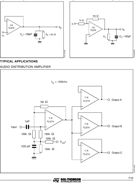
-AUDIO DISTRIBUTION AMPLIFIER
-TYPICAL APPLICATIONS(continued) POSITIVE FEEDBACK BANDPASS FILTER
074-24.IMG
CASCADED BANDPASS F IL TER fo = 100kHz ; Q = 69 ; Gain = 16
OUTPUT B
074-23.IMG
SECOND ORDER BANDPASS F ILT ER fo = 100kHz ; Q = 30 ; G ain = 16
OUTPUT A
PM-DIP14.EPS
PACKAGE MECHANICAL DATA
14 PINS - PL ASTIC DIP OR CERDIP
Dimensions Millimeters Inches
Min. Typ. Max. Min. Typ. Max.
a1 0.51 0.020
B 1.39 1.65 0.055 0.065
b 0.5 0.020
b1 0.25 0.010
D 20 0.787
E 8.5 0.335
e 2.54 0.100
e3 15.24 0.600
F 7.1 0.280
i 5.1 0.201
L 3.3 0.130
Z 1.27 2.54 0.050 0.100 DIP14.TBL
PM-SO14.EPS
PACKAGE MECHANICAL DATA
14 PINS - PL ASTIC MICROPACKAGE (SO)
Dimensions Millimeters Inches
Min. Typ. Max. Min. Typ. Max.
A 1.75 0.069
a1 0.1 0.2 0.004 0.008
a2 1.6 0.063
b 0.35 0.46 0.014 0.018
b1 0.19 0.25 0.007 0.010
C 0.5 0.020
c1 45o(typ.)
D 8.55 8.75 0.336 0.334
E 5.8 6.2 0.228 0.244
e 1.27 0.050
e3 7.62 0.300
F 3.8 4.0 0.150 0.157
G 4.6 5.3 0.181 0.208
L 0.5 1.27 0.020 0.050
M 0.68 0.027
S 8o(max.) SO14.TBL
Information furnished is believed to be accurate and reliable. However, SGS-THOMSON Microelectronics assumes no responsi-bility for the consequences of use of such information nor for any infringement of patents or other rights of third parties which may result from its use. No licence is granted by implication or otherwise under any patent or patent rights of SGS-THOMSON Microelectronics. Specifications mentioned in this publ ication are subject to change without notice. This pub lication supersedes and replaces all information previously supplied. SGS-THOMSON Microelectronics products are not authorized for use as critical components in life support devices or systems without express written approval of SGS-THOMSON Microelectronics.
1996 SGS-THOMSON Microelectronics - All Rights Reserved
SGS-THOMSON Microelectronics GROUP OF COMPANIES
Australia - Brazil - France - Germany - Hong Kong - Italy - Japan - Korea - Malaysia - Malta - Morocco - The Netherlands
CODE
: