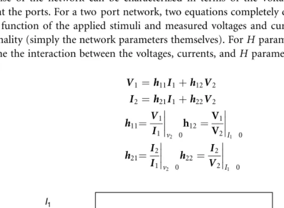
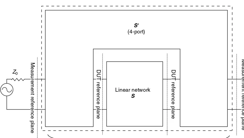
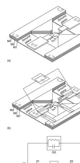
Measurement and
Modeling of Silicon
Heterostructure
Edited by
John D. Cressler
CRC Press is an imprint of the
Taylor & Francis Group, an informa business Boca Raton London New York
Measurement and
Modeling of Silicon
Heterostructure
CRC Press
Taylor & Francis Group
6000 Broken Sound Parkway NW, Suite 300 Boca Raton, FL 33487-2742
© 2008 by Taylor & Francis Group, LLC
CRC Press is an imprint of Taylor & Francis Group, an Informa business No claim to original U.S. Government works
Printed in the United States of America on acid-free paper 10 9 8 7 6 5 4 3 2 1
International Standard Book Number-13: 978-1-4200-6692-0 (Hardcover)
This book contains information obtained from authentic and highly regarded sources. Reprinted material is quoted with permission, and sources are indicated. A wide variety of references are listed. Reasonable efforts have been made to publish reliable data and information, but the author and the publisher cannot assume responsibility for the validity of all materials or for the consequences of their use.
Except as permitted under U.S. Copyright Law, no part of this book may be reprinted, reproduced, transmitted, or uti-lized in any form by any electronic, mechanical, or other means, now known or hereafter invented, including photocopy-ing, microfilmphotocopy-ing, and recordphotocopy-ing, or in any information storage or retrieval system, without written permission from the publishers.
For permission to photocopy or use material electronically from this work, please access www.copyright.com (http:// www.copyright.com/) or contact the Copyright Clearance Center, Inc. (CCC) 222 Rosewood Drive, Danvers, MA 01923, 978-750-8400. CCC is a not-for-profit organization that provides licenses and registration for a variety of users. For orga-nizations that have been granted a photocopy license by the CCC, a separate system of payment has been arranged. Trademark Notice: Product or corporate names may be trademarks or registered trademarks, and are used only for identification and explanation without intent to infringe.
Library of Congress Cataloging-in-Publication Data
Measurement and modeling of silicon heterostructure devices / editor, John D. Cressler. p. cm.
Includes bibliographical references and index. ISBN 978-1-4200-6692-0 (alk. paper)
1. Bipolar transistors--Mathematical models. 2. Bipolar transistors. 3. Heterostructures. 4. Integrated circuits--Design and construction. I. Cressler, John D.
TK7871.96.B55M33 2008
621.3815’2--dc22 2007030737
Visit the Taylor & Francis Web site at http://www.taylorandfrancis.com
Of the many dedicated scientists and engineers Who helped create this field and make it a success. I tip my hat, and offer sincere thanks from all of us Who have benefitted from your keen insights and imaginings.
And . . .
For Maria:
My beautiful wife, best friend, and soul mate for these 25 years. For Matthew John, Christina Elizabeth, and Joanna Marie: God’s awesome creations, and our precious gifts.
He Whose Heart Has Been Set
On The Love Of Learning And True Wisdom
And Has Exercised This Part of Himself,
That Man Must Without Fail Have Thoughts
That Are Immortal And Divine,
If He Lay Hold On Truth.
Plato
¯Œ ı Ø Ø
łı ı `ª ªØÆ Ł
ŒÆØ `ºŁØ Æ
,
ŒÆØ Ø `ŒŁ ªØÆ
,
‚Æ Ø ¢ æÆ æ
ø ºº Æ ŒØ ŒłØ
`ŁÆ ŒÆØ ¨
,
¯ æØŁ `ºŁØÆ
.
Foreword
Progress in a given field of technology is both desired and expected to follow a stable and predictable long term trajectory. Semilog plots of technology trends spanning decades in time and orders of magnitude in value abound. Perhaps the most famous exemplar of such a technology trajectory is the trend line associated with Moore’s law, where technology density has doubled every 12 to 18 months for several decades. One must not, however, be lulled into extrapolating such predictability to other aspects of semiconductor technology, such as device performance, or even to the long term prospects for the continuance of device density scaling itself. New physical phenomena assert themselves as one approaches the limits of a physical system, as when device layers approach atomic dimensions, and thus, no extrapolation goes on indefinitely.
Technology density and performance trends, though individually constant over many years, are the result of an enormously complex interaction between a series of decisions made as to the layout of a given device, the physics behind its operation, manufacturability considerations, and its extensibility into the future. This complexity poses a fundamental challenge to the device physics and engineering community, which must delve as far forward into the future as possible to understand when physical law precludes further progress down a given technology path. The early identification of such impending technological discontinuities, thus providing time to ameliorate their consequences, is in fact vital to the health of the semiconductor industry. Recently disrupted trends in CMOS microprocessor performance, where the ‘‘value’’ of processor operating frequency was suddenly subordinated to that of integration, demonstrate the challenges remaining in accurately assessing the behavior of future technologies. However, current challenges faced in scaling deep submicron CMOS technology are far from unique in the history of semiconductors.
Bipolar junction transistor (BJT) technology, dominant in high end computing applications during the mid 1980s, was being aggressively scaled to provide the requisite performance for future systems. By the virtue of bipolar transistors being vertical devices rather than lateral (as CMOS is), the length scale of bipolar transistors is set by the ability to control layer thicknesses rather than lateral dimensions. This allowed the definition of critical device dimensions, such as base width, to values far below the limits of optical lithography of the day. Although great strides in device performance had been made by 1985, with unity gain cutoff frequencies (fT) in the range 20 30 GHz seemingly feasible, device scaling was
approaching limits at which new physical phenomena became significant. Highly scaled silicon BJTs, having base widths below 1000 A˚, demonstrated inordinately high reverse junction leakage. This was due to the onset of band to band tunneling between heavily doped emitter and base regions, rendering such devices unreliable. This and other observations presaged one of the seminal technology discontinuities of the past decade, silicon germanium (SiGe) heterojunction bipolar transistor (HBT) technology being the direct consequence.
Begun as a program to develop bipolar technology with performance capabilities well beyond those possible via the continued scaling of conventional Si BJTs, SiGe HBT technology has found a wealth of applications beyond the realm of computing. A revolution in bipolar fabrication methodology, moving
from device definition by implantation to device deposition and definition by epitaxy, accompanied by the exploitation of bandgap tailoring, took silicon based bipolar transistor performance to levels never anticipated. It is now common to find SiGe HBTs with performance figures in excess of 300 GHz for bothfTandfmax, and circuits operable at frequencies in excess of 100 GHz.
A key observation is that none of this progress occurred in a vacuum, other than perhaps in the field of materials deposition. The creation of a generation of transistor technology having tenfold improved performance would of itself have produced far less ultimate value in the absence of an adequate eco system to enable its effective creation and utilization. This text is meant to describe the eco system that developed around SiGe technology as context for the extraordinary achievement its commercial rollout represented.
Early SiGe materials, of excellent quality in the context of fundamental physical studies, proved near useless in later device endeavors, forcing dramatic improvements in layer control and quality to then enable further development. Rapid device progress that followed drove silicon based technology (recall that SiGe technology is still a silicon based derivative) to unanticipated performance levels, demanding the development of new characterization and device modeling techniques. As materials work was further proven SiGe applications expanded to leverage newly available structural and chemical control.
Devices employing ever more sophisticated extensions of SiGe HBT bandgap tailoring have emerged, utilizing band offsets and the tailoring thereof to create SiGe based HEMTs, tunneling devices, mobility enhanced CMOS, optical detectors, and more to come. Progress in these diverse areas of device design is timely, as I have already noted the now asymptotic nature of performance gains to be had from continued classical device scaling, leading to a new industry focus on innovation rather than pure scaling. Devices now emerging in SiGe are not only to be valued for their performance, but rather their variety of functionality, where, for example, optically active components open up the prospect of the seamless integration of broadband communication functionality at the chip level.
Access to high performance SiGe technology has spurred a rich diversity of exploratory and com mercial circuit applications, many elaborated in this text. Communications applications have been most significantly impacted from a commercial perspective, leveraging the ability of SiGe technologies to produce extremely high performance circuits while using back level, and thus far less costly, fabricators than alternative materials such as InP, GaAs, or in some instances advanced CMOS.
These achievements did not occur without tremendous effort on the part of many workers in the field, and the chapters in this volume represent examples of such contributions. In its transition from scientific curiosity to pervasive technology, SiGe based device work has matured greatly, and I hope you find this text illuminating as to the path that maturation followed.
Bernard S. Meyerson
Preface
While the idea of cleverly using silicon germanium (SiGe) and silicon (Si) strained layer epitaxy to practice bandgap engineering of semiconductor devices in the highly manufacturable Si material system is an old one, only in the past decade has this concept become a practical reality. The final success of creating novel Si heterostructure transistors with performance far superior to their Si only homojunction cousins, while maintaining strict compatibility with the massive economy of scale of conventional Si integrated circuit manufacturing, proved challenging and represents the sustained efforts of literally thousands of physicists, electrical engineers, material scientists, chemists, and technicians across the world. In the electronics domain, the fruit of that global effort is SiGe heterojunction bipolar transistor (SiGe HBT) BiCMOS technology, and strained Si/SiGe CMOS technology, both of which are at present in commercial manufacturing worldwide and are rapidly finding a number of important circuit and system applications. As with any new integrated circuit technology, the industry is still actively exploring device performance and scaling limits (at present well above 300 GHz in frequency response, and rising), new circuit applications and potential new markets, as well as a host of novel device and structural innovations. This commercial success in the electronics arena is also spawning successful forays into the optoelectronics and even nanoelectronics fields. The Si heterostructure field is both exciting and dynamic in its scope.
The implications of the Si heterostructure success story contained in this book are far ranging and will be both lasting and influential in determining the future course of the electronics and optoelectronics infrastructure, fueling the miraculous communications explosion of the twenty first century. While several excellent books on specific aspects of the Si heterostructures field currently exist (for example, on SiGe HBTs), this is the first reference book of its kind that ‘‘brings it all together,’’ effectively presenting a comprehensive perspective by providing very broad topical coverage ranging from materials, to fabrication, to devices (HBT, FET, optoelectronic, and nanostructure), to CAD, to circuits, to applica tions. Each chapter is written by a leading international expert, ensuring adequate depth of coverage, up to date research results, and a comprehensive list of seminal references. A novel aspect of this book is that it also contains ‘‘snap shot’’ views of the industrial ‘‘state of the art,’’ for both devices and circuits, and is designed to provide the reader with a useful basis of comparison for the current status and future course of the global Si heterostructure industry.
This book is intended for a number of different audiences and venues. It should prove to be a useful resource as:
1. A hands on reference for practicing engineers and scientists working on various aspects of Si heterostructure integrated circuit technology (both HBT, FET, and optoelectronic), including materials, fabrication, device physics, transistor optimization, measurement, compact modeling and device simulation, circuit design, and applications
2. A hands on research resource for graduate students in electrical and computer engineering, physics, or materials science who require information on cutting edge integrated circuit technologies
3. A textbook for use in graduate level instruction in this field
4. A reference for technical managers and even technical support/technical sales personnel in the semiconductor industry
It is assumed that the reader has some modest background in semiconductor physics and semiconductor devices (at the advanced undergraduate level), but each chapter is self contained in its treatment.
In this age of extreme activity, in which we are all seriously pressed for time and overworked, my success in getting such a large collection of rather famous people to commit their precious time to my vision for this project was immensely satisfying. I am happy to say that my authors made the process quite painless, and I am extremely grateful for their help. The list of contributors to this book actually reads like a global ‘‘who’s who’’ of the silicon heterostructure field, and is impressive by any standard. I would like to formally thank each of my colleagues for their hard work and dedication to executing my vision of producing a lasting Si heterostructure ‘‘bible.’’ In order of appearance, the ‘‘gurus’’ of our field include:
Robert A. Groves, IBM Microelectronics, USA David C. Sheridan, IBM Microelectronics, USA Jeffrey B. Johnson, IBM Microelectronics, USA Rajendran Krishnasamy, IBM Microelectronics, USA Michael Schro¨ter, University of California at San Diego, USA
Slobodan Mijalkovic´, Delft University of Technology, The Netherlands Sue E. Strang, IBM Microelectronics, USA
Raminderpal Singh, IBM Systems and Technology Group, USA Youri V. Tretiakov, RF Micro Devices, USA
Qingqing Liang, Georgia Institute of Technology, USA Ramana M. Malladi, IBM Microelectronics, USA
I would also like to thank my graduate students and post docs, past and present, for their dedication and tireless work in this fascinating field. I rest on their shoulders. They include: David Richey, Alvin Joseph, Bill Ansley, Juan Rolda´n, Stacey Salmon, Lakshmi Vempati, Jeff Babcock, Suraj Mathew, Kartik Jayanaraynan, Greg Bradford, Usha Gogineni, Gaurab Banerjee, Shiming Zhang, Krish Shivaram, Dave Sheridan, Gang Zhang, Ying Li, Zhenrong Jin, Qingqing Liang, Ram Krithivasan, Yun Luo, Tianbing Chen, Enhai Zhao, Yuan Lu, Chendong Zhu, Jon Comeau, Jarle Johansen, Joel Andrews, Lance Kuo, Xiangtao Li, Bhaskar Banerjee, Curtis Grens, Akil Sutton, Adnan Ahmed, Becca Haugerud, Mustayeen Nayeem, Mustansir Pratapgarhwala, Guofu Niu, Emery Chen, Jongsoo Lee, and Gnana Prakash.
Finally, I am grateful to Tai Soda at Taylor & Francis for talking me into this project, and supporting me along the way. I would also like to thank the production team at Taylor & Francis for their able assistance (and patience!), especially Jessica Vakili.
The many nuances of the Si heterostructure field make for some fascinating subject matter, but this is no mere academic pursuit. In the grand scheme of things, the Si heterostructure industry is already reshaping the global communications infrastructure, which is in turn dramatically reshaping the way life on planet Earth will transpire in the twenty first century and beyond. The world would do well to pay attention. It has been immensely satisfying to see both the dream of Si/SiGe bandgap engineering, and this book, come to fruition. I hope our efforts please you. Enjoy!
John D. Cressler
Editor
John D. Cresslerreceived a B.S. in physics from the Georgia Institute of Technology (Georgia Tech), Atlanta, Georgia, in 1984, and an M.S. and Ph.D. in applied physics from Columbia University, New York, in 1987 and 1990. From 1984 to 1992 he was on the research staff at the IBM Thomas J. Watson Research Center in Yorktown Heights, New York, working on high speed Si and SiGe bipolar devices and technology. In 1992 he left IBM Research to join the faculty at Auburn University, Auburn, Alabama, where he served until 2002. When he left Auburn University, he was Philpott Westpoint Stevens Distinguished Professor of Electrical and Computer Engineering and director of the Alabama Microelectronics Science and Technology Center.
In 2002, Dr. Cressler joined the faculty at Georgia Tech, where he is currently Ken Byers Professor of Electrical and Computer Engineering. His research interests include SiGe devices and technology; Si based RF/microwave/millimeter wave mixed signal devices and circuits; radiation effects; device circuit interactions; noise and linearity; reliability physics; extreme environment electronics, 2 D/3 D device level simulation; and compact circuit modeling. He has published more than 350 technical papers related to his research, and is author of the books Silicon Germanium Heterojunction Bipolar Transistors, Artech House, 2003 (with Guofu Niu), andReinventing Teenagers: The Gentle Art of Instilling Character in Our Young People, Xlibris, 2004 (a slightly different genre!).
Dr. Cressler was Associate Editor of theIEEE Journal of Solid State Circuits(1998 2001), Guest Editor of theIEEE Transactions on Nuclear Science(2003 2006), and Associate Editor of theIEEE Transactions on Electron Devices (2005 present). He served on the technical program committees of the IEEE International Solid State Circuits Conference (1992 1998, 1999 2001), the IEEE Bipolar/BiCMOS Circuits and Technology Meeting (1995 1999, 2005 present), the IEEE International Electron Devices Meeting (1996 1997), and the IEEE Nuclear and Space Radiation Effects Conference (1999 2000, 2002 2007). He currently serves on the executive steering committee for the IEEE Topical Meeting on Silicon Monolithic Integrated Circuits in RF Systems, as international program advisor for the IEEE European Workshop on Low Temperature Electronics, on the technical program committee for the IEEE Inter national SiGe Technology and Device Meeting, and as subcommittee chair of the 2004 Electrochemical Society Symposium of SiGe: Materials, Processing, and Devices. He was the Technical Program Chair of the 1998 IEEE International Solid State Circuits Conference, the Conference Co Chair of the 2004 IEEE Topical Meeting on Silicon Monolithic Integrated Circuits in RF Systems, and the Technical Program Chair of the 2007 IEEE Nuclear and Space Radiation Effects Conference.
Dr. Cressler was appointed an IEEE Electron Device Society Distinguished Lecturer in 1994, an IEEE Nuclear and Plasma Sciences Distinguished Lecturer in 2006, and was awarded the 1994 Office of Naval Research Young Investigator Award for his SiGe research program. He received the 1996 C. Holmes
MacDonald National Outstanding Teacher Award by Eta Kappa Nu, the 1996 Auburn University Alumni Engineering Council Research Award, the 1998 Auburn University Birdsong Merit Teaching Award, the 1999 Auburn University Alumni Undergraduate Teaching Excellence Award, an IEEE Third Millennium Medal in 2000, and the 2007 Georgia Tech Outstanding Faculty Leadership in the Development of Graduate Students Award. He is an IEEE Fellow.
On a more personal note, John’s hobbies include hiking, gardening, bonsai, all things Italian, collecting (and drinking!) fine wines, cooking, history, and carving walking sticks, not necessarily in that order. He considers teaching to be his vocation. John has been married to Maria, his best friend and soul mate, for 25 years, and is the proud father of three budding scholars: Matt, Christina, and Jo Jo.
Contents
1 The Big Picture ... 1-1
John D. Cressler
2 A Brief History of the Field ... 2-1
John D. Cressler
3 Overview: Measurement and Modeling ... 3-1
John D. Cressler
4 Best-Practice AC Measurement Techniques... 4-1
Robert A. Groves
5 Industrial Application of TCAD for SiGe Development ... 5-1
David C. Sheridan, Jeffrey B. Johnson, and Rajendran Krishnasamy
6 Compact Modeling of SiGe HBTs: HICUM ... 6-1
Michael Schro¨ter
7 Compact Modeling of SiGe HBTs: Mextram ... 7-1
Slobodan Mijalkovic´
8 CAD Tools and Design Kits ... 8-1
Sue E. Strang
9 Parasitic Modeling and Noise Mitigation Approaches in Silicon Germanium RF Designs .... 9-1
Raminderpal Singh
10 Transmission Lines on Si... 10-1
Youri V. Tretiakov
11 Improved De-Embedding Techniques ... 11-1
Qingqing Liang
A.1 Properties of Silicon and Germanium ... A.1-1
John D. Cressler
A.2 The Generalized Moll Ross Relations ... A.2-1
John D. Cressler
A.3 Integral Charge-Control Relations ... A.3-1
Michael Schro¨ter
A.4 Sample SiGe HBT Compact Model Parameters... A.4-1
Ramana M. Malladi
Index ... I-1
1
The Big Picture
John D. Cressler
Georgia Institute of Technology
1.1 The Communications Revolution...11 1.2 Bandgap Engineering in the Silicon
Material System ...13 1.3 Terminology and Definitions ...14 1.4 The Application Space ...15 1.5 Performance Limits and Future Directions ...19
1.1 The Communications Revolution
We are at a unique juncture in the history of humankind, a juncture that amazingly we engineers and scientists have dreamed up and essentially created on our own. This pivotal event can be aptly termed the ‘‘Communications Revolution,’’ and the twenty first century, our century, will be the era of human history in which this revolution plays itself out.
This communications revolution can be functionally defined and characterized by the pervasive acquisition, manipulation, storage, transformation, and transmission of ‘‘information’’ on a global scale. This information, or more generally, knowledge, in its infinitely varied forms and levels of complexity, is gathered from our analog sensory world, transformed in very clever ways into logical ‘‘1’’s and ‘‘0’’s for ease of manipulation, storage, and transmission, and subsequently regenerated into analog sensory output for our use and appreciation. In 2005, this planetary communication of information is occurring at a truly mind numbing rate, estimates of which are on the order of 80 Tera bits/sec (1012) of data transfer across the globe in 2005 solely in wired and wireless voice and data transmission, 24 hours a day, 7 days a week, and growing exponentially. The world is quite literally abuzz with information flow communication.*It is for the birth of the Communications Revolution that we humans likely will be remembered for 1000 years hence. Given that this revolution is happening during the working careers of most of us, I find it a wonderful time to be alive, a fact of which I remind my students often.
Here is my point. No matter how one slices it, at the most fundamental level, it is semiconductor devices that are powering this communications revolution. Skeptical? Imagine for a moment that one could flip a switch and instantly remove all of the integrated circuits (ICs) from planet Earth. A moment’s reflection will convince you that there is not a single field of human endeavor that would not come to a grinding halt, be it commerce, or agriculture, or education, or medicine, or entertain ment. Life as we in the first world know it in 2005 would simply cease to exist. And yet, remarkably, the same result would not have been true 50 years ago; even 20 years ago. Given the fact that we humans have been on planet Earth in our present form for at least 1 million years, and within communities
*I have often joked with my students that it would be truly entertaining if the human retina was sensitive to longer wavelengths of electromagnetic radiation, such that we could ‘‘see’’ all the wireless communications signals constantly bathing the planet (say, in greens and blues!). It might change our feelings regarding our ubiquitous cell phones!
having entrenched cultural traditions for at least 15,000 years, this is truly a remarkable fact of history. A unique juncture indeed.
Okay, hold on tight. It is an easy case to make that the semiconductor silicon (Si) has single handedly enabled this communications revolution.* I have previously extolled at length the remarkable virtues of this rather unglamorous looking silver grey element [1], and I will not repeat that discussion here, but suffice it to say that Si represents an extremely unique material system that has, almost on its own, enabled the conception and evolving execution of this communications revolution. The most compel ling attribute, by far, of Si lies in the economy of scale it facilitates, culminating in the modern IC fabrication facility, effectively enabling the production of gazillions of low cost, very highly integrated, remarkably powerful ICs, each containing millions of transistors; ICs that can then be affordably placed into widgets of remarkably varied form and function.y
So what does this have to do with the book you hold in your hands? To feed the emerging infrastructure required to support this communications revolution, IC designers must work tirelessly to support increasingly higher data rates, at increasingly higher carrier frequencies, all in the design space of decreasing form factor, exponentially increasing functionality, and at ever decreasing cost. And by the way, the world is going portable and wireless, using the same old wimpy batteries. Clearly, satisfying the near insatiable appetite of the requisite communications infrastructure is no small task. Think of it as job security!
For long term success, this quest for more powerful ICs must be conducted within the confines of conventional Si IC fabrication, so that the massive economy of scale of the global Si IC industry can be brought to bear. Therein lies the fundamental motivation for the field of Si heterostructures, and thus this book. Can one use clever nanoscale engineering techniques to custom tailor the energy bandgap of fairly conventional Si based transistors to: (a) improve their performance dramatically and thereby ease the circuit and system design constraints facing IC designers, while (b) performing this feat without throwing away all the compelling economy of scale virtues of Si manufacturing? The answer to this important question is a resounding ‘‘YES!’’ That said, getting there took time, vision, as well as dedication and hard work of literally thousands of scientists and engineers across the globe.
In the electronics domain, the fruit of that global effort is silicon germanium heterojunction bipolar transistor (SiGe HBT) bipolar complementary metal oxide semiconductor (BiCMOS) technology, and is in commercial manufacturing worldwide and is rapidly finding a number of important circuit and system applications. In 2004, the SiGe ICs, by themselves, are expected to generate US$1 billion in revenue globally, with perhaps US$30 billion in downstream products. This US$1 billion figure is projected to rise to US$2.09 billion by 2006 [2], representing a growth rate of roughly 42% per year, a remarkable figure by any economic standard. The biggest single market driver remains the cellular industry, but applications in optical networking, hard disk drives for storage, and automotive collision avoidance radar systems are expected to represent future high growth areas for SiGe. And yet, in the beginning of 1987, only 18 years ago, there was no such thing as a SiGe HBT. It had not been demonstrated as a viable concept. An amazing fact.
In parallel with the highly successful development of SiGe HBT technology, a wide class of ‘‘transport enhanced’’ field effect transistor topologies (e.g., strained Si CMOS) have been developed as a means to boost the performance of the CMOS side of Si IC coin, and such technologies have also recently begun
*The lone exception to this bold claim lies in the generation and detection of coherent light, which requires direct bandgap III V semiconductor devices (e.g., GaAs of InP), and without which long haul fiber communications systems would not be viable, at least for the moment.
yConsider: it has been estimated that in 2005 there are roughly 20,000,000,000,000,000,000 (21019) transistors
to enter the marketplace as enhancements to conventional core CMOS technologies. The commercial success enjoyed in the electronics arena has very naturally also spawned successful forays into the optoelectronics and even nanoelectronics fields, with potential for a host of important downstream applications.
The Si heterostructure field is both exciting and dynamic in its scope. The implications of the Si heterostructure success story contained in this book are far ranging and will be both lasting and influential in determining the future course of the electronics and optoelectronics infrastructure, fueling the miraculous communications explosion of our twenty first century. The many nuances of the Si hetero structure field make for some fascinating subject matter, but this is no mere academic pursuit. As I have argued, in the grand scheme of things, the Si heterostructure industry is already reshaping the global communications infrastructure, which is in turn dramatically reshaping the way life of planet Earth will transpire in the twenty first century and beyond. The world would do well to pay close attention.
1.2 Bandgap Engineering in the Silicon Material System
As wonderful as Si is from a fabrication viewpoint, from a device or circuit designer’s perspective, it is hardly the ideal semiconductor. The carrier mobility for both electrons and holes in Si is comparatively small compared to their III V cousins, and the maximum velocity that these carriers can attain under high electric fields is limited to about 1107cm/sec under normal conditions, relatively ‘‘slow.’’ Since
the speed of a transistor ultimately depends on how fast the carriers can be transported through the device under sustainable operating voltages, Si can thus be regarded as a somewhat ‘‘meager’’ semicon ductor. In addition, because Si is an indirect gap semiconductor, light emission is fairly inefficient, making active optical devices such as diode lasers impractical (at least for the present). Many of the III V compound semiconductors (e.g., GaAs or InP), on the other hand, enjoy far higher mobilities and saturation velocities, and because of their direct gap nature, generally make efficient optical generation and detection devices. In addition, III V devices, by virtue of the way they are grown, can be compositionally altered for a specific need or application (e.g., to tune the light output of a diode laser to a specific wavelength). This atomic level custom tailoring of a semiconductor is called bandgap engineering, and yields a large performance advantage for III V technologies over Si [3]. Unfortunately, these benefits commonly associated with III V semiconductors pale in comparison to the practical deficiencies associated with making highly integrated, low cost ICs from these materials. There is no robust thermally grown oxide for GaAs or InP, for instance, and wafers are smaller with much higher defect densities, are more prone to breakage, and are poorer heat conductors (the list could go on). These deficiencies translate into generally lower levels of integration, more difficult fabrication, lower yield, and ultimately higher cost. In truth, of course, III V materials such as GaAs and InP fill important niche markets today (e.g., GaAs metal semiconductor field effect transistor (MESFETs) and HBTs for cell phone power amplifiers, AlGaAs or InP based lasers, efficient long wavelength photodetectors, etc.), and will for the foreseeable future, but III V semiconductor technologies will never become mainstream in the infrastructure of the communications revolution if Si based technologies can do the job.
While Si ICs are well suited to high transistor count, high volume microprocessors and memory applications, RF, microwave, and even millimeter wave (mm wave) electronic circuit applications, which by definition operate at significantly higher frequencies, generally place much more restrictive performance demands on the transistor building blocks. In this regime, the poorer intrinsic speed of Si devices becomes problematic. That is, even if Si ICs are cheap, they must deliver the required device and circuit performance to produce a competitive system at a given frequency. If not, the higher priced but faster III V technologies will dominate (as they indeed have until very recently in the RF and microwave markets).
associated with using SiGe and Si strained layer epitaxy to practice bandgap engineering in the Si material system, a process culminating in, among other things, the SiGe HBT and strained Si CMOS, as well as a variety of other interesting electronic and optoelectronic devices built from these materials. This totality can be termed the ‘‘Si heterostructures’’ field.
1.3 Terminology and Definitions
A few notes on modern usage and pronunciation in this field are in order (really!). It is technically correct to refer to silicon germanium alloys according to their chemical composition, Si1xGex, wherex
is the Ge mole fraction. Following standard usage, such alloys are generally referred to as ‘‘SiGe’’ alloys. Note, however, that it is common in the material science community to also refer to such materials as ‘‘Ge:Si’’ alloys.
A SiGe film that is carbon doped (e.g., less than 0.20% C) in an attempt to suppress subsequent boron out diffusion (e.g., in HBTs) is properly referred to as a SiGe:C alloy, or simply SiGeC (pronounced ‘‘silicon germanium carbon,’’ not ‘‘silicon germanium carbide’’). This class of SiGe alloys should be viewed as optimized SiGe alloys, and are distinct from SiGe films with a much higher C content (e.g., 2% to 3% C) that might be used, for instance, to lattice match SiGeC alloys to Si.
Believe it or not, this field also has its own set of slang pronunciations. The colloquial usage of the pronunciation \’sig ee\ to refer to ‘‘silicon germanium’’ (begun at IBM in the late 1990s) has come into vogue (heck, it may make it to the dictionary soon!), and has even entered the mainstream IC engineers’s slang; pervasively.*
In the electronics domain, it is important to be able to distinguish between the various SiGe technologies as they evolve, both for CMOS (strained Si) and bipolar (SiGe HBT). Relevant questions in this context include: Is company X’s SiGe technology more advanced than company Y’s SiGe technology? For physical as well as historical reasons, one almost universally defines CMOS technology (Si, strained Si, or SiGe), a lateral transport device, by the drawn lithographic gate length (the CMOS technology ‘‘node’’), regardless of the resultant intrinsic device performance. Thus, a ‘‘90 nm’’ CMOS node has a drawn gate length of roughly 90 nm. For bipolar devices (i.e., the SiGe HBT), however, this is not so straightforward, since it is a vertical transport device whose speed is not nearly as closely linked to lithographic dimensions.
In the case of the SiGe HBT it is useful to distinguish between different technology generations according to their resultant acperformance (e.g., peak common emitter, unity gain cutoff frequency (fT), which is (a) easily measured and unambiguously compared technology to technology, and yet is (b)
a very strong function of the transistor vertical doping and Ge profile and hence nicely reflects the degree of sophistication in device structural design, overall thermal cycle, epi growth, etc.) [1]. The peak fT
generally nicely reflects the ‘‘aggressiveness,’’ if you will, of the transistor scaling which has been applied to a given SiGe technology. A higher level of comparative sophistication can be attained by also invoking the maximum oscillation frequency (fmax), a parameter which is well correlated to both intrinsic profile
and device parasitics, and hence a bit higher on the ladder of device performance metrics, and thus more representative of actual large scale circuit performance. The difficulty in this case is thatfmaxis far more
ambiguous thanfT, in the sense that it can be inferred from various gain definitions (e.g., U vs. MAG),
and in practice power gain data are often far less ideal in its behavior over frequency, more sensitive to accurate deembedding, and ripe with extraction ‘‘issues.’’
We thus term a SiGe technology having a SiGe HBT with a peakfTin the range of 50 GHz as ‘‘first
generation;’’ that with a peakfTin the range of 100 GHz as ‘‘second generation;’’ that with a peakfTin
the range of 200 GHz as ‘‘third generation;’’ and that with a peakfTin the range of 300 GHz as ‘‘fourth
generation.’’ These are loose definitions to be sure, but nonetheless useful for comparison purposes.
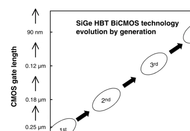
A complicating factor in SiGe technology terminology results from the fact that most, if not all, commercial SiGe HBT technologies today also contain standard Si CMOS devices (i.e., SiGe HBT BiCMOS technology) to realize high levels of integration and functionality on a single die (e.g., single chip radios complete with RF front end, data converters, and DSP). One can then speak of a given generation of SiGe HBT BiCMOS technology as the most appropriate intersection of both the SiGe HBT peakfTand the CMOS technology node (Figure 1.1). For example, for several commercially important
SiGe HBT technologies available via foundry services, we have:
. IBM SiGe 5HP 50 GHz peakfTSiGe HBTþ0.35mm Si CMOS (first generation) . IBM SiGe 7HP 120 GHz peakfTSiGe HBTþ0.18mm Si CMOS (second generation) . IBM SiGe 8HP 200 GHz peakfTSiGe HBTþ0.13mm Si CMOS (third generation) . Jazz SiGe 60 60 GHz peakfTSiGe HBTþ0.35mm Si CMOS (first generation) . Jazz SiGe 120 150 GHz peakfTSiGe HBTþ0.18mm Si CMOS (second generation) . IHP SiGe SGC25B 120 GHz peakfTSiGe HBTþ0.25mm Si CMOS (second generation)
All SiGe HBT BiCMOS technologies can thus be roughly classified in this manner. It should also be understood that multiple transistor design points typically exist in such BiCMOS technologies (multiple breakdown voltages for the SiGe HBT and multiple threshold or breakdown voltages for the CMOS), and hence the reference to a given technology generation implicitly refers to the most aggressively scaled device within that specific technology platform.
1.4 The Application Space
It goes without saying in our field of semiconductor IC technology that no matter how clever or cool a new idea appears at first glance, its long term impact will ultimately be judged by its marketplace ‘‘legs’’ (sad, but true). That is, was the idea good for a few journal papers and an award or two, or did someone actually build something and sell some useful derivative products from it? The sad reality is that the semiconductor field (and we are by no means exceptional) is rife with examples of cool new devices that
50 GHz 100 GHz 200 GHz 300 GHz SiGe HBT peak cutoff frequency
CMOS gate length
90 nm
0.12 µm
0.18 µm
0.25 µm
1st
2nd
3rd
4th SiGe HBT BiCMOS technology evolution by generation
never made it past the pages of the IEDM digest! The ultimate test, then, is one of stamina. And sweat. Did the idea make it out of the research laboratory and into the hands of the manufacturing lines? Did it pass the qualification checkered flag, have design kits built around it, and get delivered to real circuit designers who built ICs, fabricated them, and tested them? Ultimately, were the derivative ICs inserted into real systems widgets to garner leverage in this or that system metric, and hence make the products more appealing in the marketplace?
Given the extremely wide scope of the semiconductor infrastructure fueling the communications revolution, and the sheer volume of widget possibilities, electronic to photonic to optoelectronic, it is useful here to briefly explore the intended application space of Si heterostructure technologies as we peer out into the future. Clearly I possess no crystal ball, but nevertheless some interesting and likely lasting themes are beginning to emerge from the fog.
SiGe HBT BiCMOS is the obvious ground breaker of the Si heterostructures application space in terms of moving the ideas of our field into viable products for the marketplace. The field is young, but the signs are very encouraging. As can be seen in Figure 1.2, there are at present count 25þSiGe HBT industrial fabrication facilities on line in 2005 around the world, and growing steadily. This trend points to an obvious recognition that SiGe technology will play an important role in the emerging electronics infrastructure of the twenty first century. Indeed, as I often point out, the fact that virtually every major player in the communications electronics field either: (a) has SiGe up and running in house, or (b) is using someone else’s SiGe fab as foundry for their designers, is a remarkable fact, and very encouraging in the grand scheme of things. As indicated above, projections put SiGe ICs at a US$2.0 billion level by 2006, small by percentage perhaps compared to the near trillion dollar global electronics market, but growing rapidly.
The intended application target? That obviously depends on the company, but the simple answer is, gulp, a little bit of everything! As depicted in Figure 1.3 and Figure 1.4, the global communications landscape is exceptionally diverse, ranging from low frequency wireless (2.4 GHz cellular) to the fastest high speed wireline systems (10 and 40 Gbit/sec synchronous optical network (SONET)). Core CMOS technologies are increasingly being pushed into the lower frequency wireless space, but the compelling drive to higher carrier frequencies over time will increasingly favor SiGe technologies.
At present, SiGe ICs are making inroads into: the cellular industry for handsets [global system for mobile communications GSM, code division multiple access (CDMA), wideband CDMA (W CDMA), etc.], even for power amplifiers; various wireless local area networks (WLAN) building blocks, from components to fully integrated systems ranging from 2.4 to 60 GHz and up; ultrawide band (UWB) components; global positioning systems (GPS); wireless base stations; a variety of wireline networking products, from 2.5 to 40 Gbit/sec (and higher); data converters (D/A and A/D); high speed memories; a variety of instrumentation electronics; read channel memory storage products; core analog functions (op amps, etc.); high speed digital circuits of various flavors; radiation detector
1995 1997 1999 2001 2003
1993 2005
0 5 10 15 20 25
SiGe HBT BiCMOS Strained–Si CMOS
Year
Industrial fabrication facilities
electronics; radar systems (from 3 to 77 GHz and up); a variety space based electronics components; and various niche extreme environment components (e.g., cryogenic (77 K) hybrid superconductor semi conductor systems). The list is long and exceptionally varied this is encouraging. Clearly, however, some of these components of ‘‘everything’’ are more important than others, and this will take time to shake out.
The strength of the BiCMOS twist to SiGe ICs cannot be overemphasized. Having both the high speed SiGe HBT together on chip with aggressively scaled CMOS allows one great flexibility in system design, the depths of which is just beginning to be plumbed. While debates still rage with respect to the most cost effective partitioning at the chip and package level (system on a chip versus system in a package,
FIGURE 1.3 The global communications landscape, broken down by the various communications standards, and spanning the range of: wireless to wireline; fixed to mobile; copper to fiber; low data rate to broadband; and local area to wide area networks. WAN iswide area network, MAN ismetropolitan area network, the so called ‘‘last mile’’ access network, LAN islocal area network, and PAN ispersonal area network, the emerging in home network. (Used with the permission of Kyutae Lim.)
1 2 3 5 10 20 30 50 100
Frequency (GHz)
Bands: L S C X K u Ka
WLAN Polling
Radar
Radar Radar
GPS
Collision avoidance
ISM
W Cellular / PCS / Satellite / UWB Communications
Automotive Navigation Defense
Some application bands for SiGe ICs
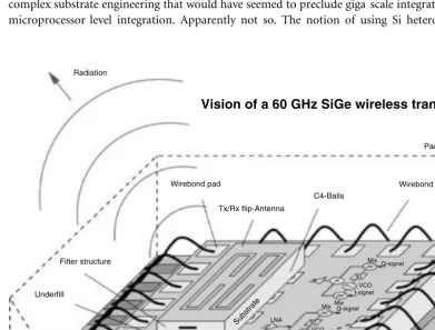
etc.), clearly increased integration is viewed as a good thing in most camps (it is just a question of how much), and SiGe HBT BiCMOS is well positioned to address such needs across a broad market sector. The envisioned high growth areas for SiGe ICs over the new few years include: the cellular industry, optical networking, disk drives, and radar systems. In addition, potential high payoff market areas span the emerging mm wave space (e.g., the 60 GHz ISM band WLAN) for short range, but very high data rate (Gbit/sec) wireless systems. A SiGe 60 GHz single chip/package transceiver (see Figure 1.5 for IBM’s vision of such a beast) could prove to be the ‘‘killer app’’ for the emerging broadband multimedia market. Laughable? No. The building blocks for such systems have already been demonstrated using third generation SiGe technology [4], and fully integrated transceivers are under development.
The rest of the potential market opportunities within the Si heterostructures field can be leveraged by successes in the SiGe IC field, both directly and indirectly. On the strained Si CMOS front, there are existent proofs now that strained Si is likely to become a mainstream component of conventional CMOS scaling at the 90 nm node and beyond (witness the early success of Intel’s 90 nm logic technology built around uniaxially strained Si CMOS; other companies are close behind). Strained Si would seem to represent yet another clever technology twist that CMOS device technologists are pulling from their bag of tricks to keep the industry on a Moore’s law growth path. This was not an obvious development (to me anyway) even a couple of years back. A wide variety of ‘‘transport enhanced’’ Si heterostructure based FETs have been demonstrated (SiGe channel FETs, Si based high electron mobility transistors (HEMTs), as well as both uniaxially and biaxially strained FETs, etc). Most of these devices, however, require complex substrate engineering that would have seemed to preclude giga scale integration level needs for microprocessor level integration. Apparently not so. The notion of using Si heterostructures (either
Vision of a 60 GHz SiGe wireless transceiver Radiation
Wirebond pad
Filter structure
Substrate Underfill
Wirebond
Tx/Rx flip-Antenna
C4-Balls
Mix
Mix
Mix
Package pin
Package mold
Mix 90
90
VCO
VCO LNA
Q-signal
Q-signal I-signal
I-signal
I/Q
I/Q
QFN-package PLL
uniaxial or biaxial strain or both) to boost conventional CMOS performance appears to be an appealing path for the future, a natural merging point I suspect for SiGe strained layers found in SiGe HBT BiCMOS (which to date contains only conventional Si CMOS) and strained Si CMOS.
From the optoelectronics camp, things are clearly far less evolved, but no less interesting. A number of functional optoelectronic devices have been demonstrated in research laboratories. Near term successes in the short wavelength detector arena and light emitting diodes (LEDs) are beginning to be realized. The achievement of successful coherent light emission in the Si heterostructure system (e.g., via quantum cascade techniques perhaps) would appear to be the ‘‘killer app’’ in this arena, and research in this area is in progress. More work is needed.
1.5 Performance Limits and Future Directions
We begin with device performance limits. Just how fast will SiGe HBTs be 5 years from now? Transistor level performance in SiGe HBTs continues to rise at a truly dizzying pace, and each major conference seems to bear witness to a new performance record (Figure 1.6). Both first and second generation SiGe HBT BiCMOS technology is widely available in 2005 (who would have thought even 3 years ago that fully integrated 100þGHz Si based devices would be ‘‘routine’’ on 200 mm wafers?), and even at the 200 GHz (third generation) performance level, six companies (at last count) have achieved initial technology demonstrations, including IBM (Chapter 7), Jazz (Chapter 8), IHP (Chapter 11), ST Microelectronics (Chapter 12), Hitachi (Chapter 9), and Infineon (Chapter 10). (See Fabrication of SiGe HBT BiCMOS Technologyfor these chapters.) Several are now either available in manufacturing, or are very close (e.g., [5]). At press time, the most impressive new stake in the ground is the report (June 2004) of the newly optimized ‘‘SiGe 9T’’ technology, which simultaneously achieves 302 GHz peakfTand
306 GHz peakfmax, a clear record for any Si based transistor, from IBM (Figure 1.7) [6]. This level of
ac performance was achieved at a BVCEO of 1.6 V, a BVCBO of 5.5 V, and a current gain of 660.
Noise measurements on these devices yielded NFmin/Gassocof 0.45 dB/14 dB and 1.4 dB/8 dB at 10 and
25 GHz, respectively. Measurements of earlier (unoptimized) fourth generation IBM SiGe HBTs have yielded record values of 375 GHz peakfT[7] at 300 K and above 500 GHz peakfTat 85 K. Simulations
suggest that THz level (1000 GHz) intrinsic transistor performance is not a laughable proposition in SiGe HBTs (Chapter 16, seeSilicon Heterostructure Devices). This fact still amazes even me, the eternal optimist of SiGe performance! I, for one, firmly believe that we will see SiGe HBTs above 500 GHz peak
0.1 1.0 10 100
0 50 100 150 200 250 300 350 400
Collector current density (mA/mm2)
Cutoff frequency (GHz)
1st
2nd
3rd
4th
fT and fmax fully integrated with nanometer scale (90 nm and below) Si CMOS (possibly strained
Si CMOS) within the next 3 to 5 years.
One might logically ask, particularly within the confines of the above discussion on ultimate market relevance, why one would even attempt to build 500 GHz SiGe HBTs, other than to win a best paper award, or to trumpet that ‘‘because it’s there’’ Mount Everest mentality we engineers and scientists love so dearly. This said, if the future ‘‘killer app’’ turns out to be single chip mm wave transceiver systems with on board DSP for broadband multimedia, radar, etc., then the ability of highly scaled, highly integrated, very high performance SiGe HBTs to dramatically enlarge the circuit/system design space of the requisite mm wave building blocks may well prove to be a fruitful (and marketable) path.
Other interesting themes are emerging in the SiGe HBT BiCMOS technology space. One is the very recent emergence of complementary SiGe (C SiGe) HBT processes (npnþpnp SiGe HBTs). While very early pnp SiGe HBT prototypes were demonstrated in the early 1990s, only in the last 2 years or so have fully complementary SiGe processes been developed, the most mature of which to date is the IHP SGC25C process, which has 200 GHz npn SiGe HBTs and 80 GHz pnp SiGe HBTs (Chapter 11, see
Fabrication of SiGe HBT BiCMOS Technology). Having very high speed pnp SiGe HBTs on board presents a fascinating array of design opportunities aimed particularly at the analog/mixed signal circuit space. In fact, an additional emerging trend in the SiGe field, particularly for companies with historical pure analog circuit roots, is to target lower peakfT, but higher breakdown voltages, while simultaneously
optimizing the device for core analog applications (e.g., op amps, line drivers, data converters, etc.), designs which might, for instance, target better noise performance, and higher current gain Early voltage product than mainstream SiGe technologies. One might even choose to park that SiGe HBT platform on top of thick film SOI for better isolation properties (Chapter 13, seeFabrication of SiGe HBT BiCMOS Technology). Another interesting option is the migration of high speed vertical SiGe HBTs with very thin film CMOS compatible SOI (Chapter 5, see Fabrication of SiGe HBT BiCMOS Technology). This technology path would clearly favor the eventual integration of SiGe HBTs with strained Si CMOS, all on SOI, a seemingly natural migratory path.
If one accepts the tenet that integration is a good thing from a system level perspective, the Holy Grail in the Si heterostructure field would, in the end, appear to be the integration of SiGe HBTs for RF through mm wave circuitry (e.g., single chip mm wave transceivers complete with on chip antennae), strained Si CMOS for all DSP and memory functionality, both perhaps on SOI, Si based light emitters, SiGe HBT modulator electronics, and detectors for such light sources, together with on chip waveguides to steer the light, realized all on one Si wafer to produce a ‘‘Si based optoelectronic superchip’’ [8], that could do it all. These diverse blocks would be optional plug in modules around a core SiGe
0 50 100 150 200 250 300 350 400
0 50 100 150 200 250 300 350 400
fT + fmax = 400 GHz
fT = fmax
SiGe+SiGe: C HBT 300 K
600 GHz
200 GHz
Peak fT (GHz)
Peak
fmax
(
GHz)
HBT þ strained Si CMOS IC technology platform, perhaps with flip chip (or other) packaging techniques to join different sub die to the main superchip (e.g., for a Si based detector or laser).
I know, I know. It is not obvious that even if each of these blocks could be realized, that it would make economic sense to do so for real systems. I have no quarrel with that. I think such a Si based superchip is a useful paradigm, however, to bind together all of the clever objects we wish to ultimately build with Si heterostructures, from electronic to photonic, and maintain the vision of the one overarching constraint that guides us as we look forward keep whatever you do compatible with high volume manufacturing in Si fabrication facilities if you want to shape the path of the ensuing communications revolution. This Si based superchip clearly remains a dream at present. A realizable dream? And if realizable, commer cially viable? Who knows? Only time will tell. But it is fun to think about.
As you peruse this book you hold in your hands, which spans the whole Si heterostructure research and development space, from materials, to devices, to circuit and system applications, I think you will be amazed at both the vision, cleverness, and smashing successes of the many scientists and engineers who make up our field. Do not count us out! We are the new architects of an oh so very interesting future.
References
1. JD Cressler and G Niu.Silicon Germanium Heterojunction Bipolar Transistors. Boston, MA: Artech House, 2003.
2. ‘‘SiGe devices market to hit $2 billion in 2006,’’ article featured on CompoundSemicoductor.net, http://compoundsemiconductor.net/articles/news/8/3/22/1.
3. F Capasso. Band gap engineering: from physics and materials to new semiconductor devices.Science, 235:172 176, 1987.
4. S Reynolds, B Floyd, U Pfeiffer, and T. Zwick. 60 GHz transciever circuits in SiGe bipolar technology. Technical Digest of the IEEE International Solid State Circuits Conference, San Francisco, 2004, pp 442 443.
5. AJ Joseph, D Coolbaugh, D Harame, G Freeman, S Subbanna, M Doherty, J Dunn, C Dickey, D Greenberg, R Groves, M Meghelli, A Rylyakov, M Sorna, O Schreiber, D Herman, and T Tanji. 0.13mm 210 GHzfTSiGe HBTs expanding the horizons of SiGe BiCMOS. Technical Digest of the
IEEE International Solid State Circuits Conference, San Francisco, 2002, pp 180 182.
6. J S Rieh, D Greenberg, M Khater, KT Schonenberg, J J Jeng, F Pagette, T Adam, A Chinthakindi, J Florkey, B Jagannathan, J Johnson, R Krishnasamy, D Sanderson, C Schnabel, P Smith, A Stricker, S Sweeney, K Vaed, T Yanagisawa, D Ahlgren, K Stein, and G Freeman. SiGe HBTs for millimeter wave applications with simultaneously optimizedfTand fmax. Proceedings of the IEEE Radio Frequency
Integrated Circuits (RFIC) Symposium, Fort Worth, 2004, pp 395 398.
7. JS Rieh, B Jagannathan, H Chen, KT Schonenberg, D Angell, A Chinthakindi, J Florkey, F Golan, D Greenberg, S J Jeng, M Khater, F Pagette, C Schnabel, P Smith, A Stricker, K Vaed, R Volant, D Ahlgren, G Freeman, K Stein, and S Subbanna. SiGe HBTs with cutoff frequency of 350 GHz. Tech nical Digest of the IEEE International Electron Devices Meeting, San Francisco, 2002, pp 771 774. 8. R Soref. Silicon based photonic devices. Technical Digest of the IEEE International Solid State
2
A Brief History
of the Field
John D. Cressler
Georgia Institute of Technology
2.1 Si SiGe Strained Layer Epitaxy...21 2.2 SiGe HBTs ...23 2.3 SiGe Strained Si FETs and Other SiGe Devices ...26
In the historical record of any field of human endeavor, being ‘‘first’’ is everything. It is often said that ‘‘hindsight is 20 20,’’ and it is tempting in many cases to ascribe this or that pivotal event as ‘‘obvious’’ or ‘‘easy’’ once the answer is known. Anyone intimately involved in a creative enterprise knows, however, that it is never easy being first, and often requires more than a little luck and maneuvering. Thus the triumphs of human creativity, the ‘‘firsts,’’ should be appropriately celebrated. Still, later chroniclers often gloss over, and then eventually ignore, important (and sometimes very interesting) twists and turns, starts and stops, of the winners as well as the second and third place finishers, who in the end may in fact have influenced the paths of the winners, sometimes dramatically. The history of our field, for instance, is replete with interesting competitive battles, unusual personalities and egos, no small amount of luck, and various other fascinating historical nuances.
There is no concise history of our field available, and while the present chapter is not intended to be either exhaustive or definitive, it represents my firm conviction that the history of any field is both instructive and important for those who follow in the footsteps of the pioneers. Hopefully this brief history does not contain too many oversights or errors, and is offered as a step in the right direction for a history of pivotal events that helped shape the Si heterostructures field.
2.1 Si–SiGe Strained Layer Epitaxy
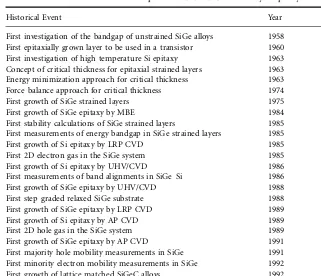
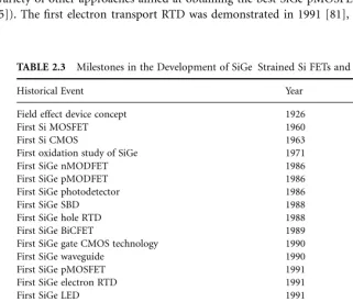
The field of Si based heterostructures solidly rests on the shoulders of materials scientists and crystal growers, those purveyors of the semiconductor ‘‘black arts’’ associated with the deposition of pristine films of nanoscale dimensionality onto enormous Si wafers with near infinite precision. What may seem routine today was not always so. The Si heterostructure story necessarily begins with materials, and circuit designers would do well to remember that much of what they take for granted in transistor performance owes a great debt to the smelters of the crystalline world. Table 2.1 summarizes the key steps in the development of SiGe Si strained layer epitaxy.
Given that Ge was the earliest and predominant semiconductor pursued by the Bell Laboratories transistor team, with a focus on the more difficult to purify Si to come slightly later, it is perhaps not surprising that the first study of SiGe alloys, albeit unstrained bulk alloys, occurred as early as 1958 [1]. It was recognized around 1960 [2] that semiconductor epitaxy*would enable more robust and control lable transistor fabrication. Once the move to Si based processing occurred, the field of Si epitaxy was
*The word ‘‘epitaxy’’ (or just ‘‘epi’’) is derived from the Greek wordepi, meaning ‘‘upon’’ or ‘‘over.’’
launched, the first serious investigation of which was reported in 1963 [3]. Early Si epitaxy was exclusively conducted under high temperature processing conditions, in the range of 11008C, a tem perature required to obtain a chemically pure and pristine growth interface on the Si host substrate for the soon to be grown crystalline Si epi. High temperature Si epi has been routinely used in basically this same form for over 40 years now, and represents a mature fabrication technique that is still widely practiced for many types of Si devices (e.g., high speed bipolar transistors and various power devices). Device engineers have long recognized the benefits of marrying the many virtues of Si as a host material for manufacturing electronic devices, with the bandgap engineering principles routinely practiced in the III V system. Ultimately this requires a means by which one can perform epitaxial deposition of thin Si layers on large Si substrates, for both p and n type doping of arbitrary abruptness, with very high precision, across large wafers, and doping control at high dynamic range. Only a moment’s reflection is required to appreciate that this means the deposition of the Si epi must occur at very low growth temperatures, say 5008C to 6008C (not ‘‘low’’ per se, but low compared to the requisite temperatures needed for solid state diffusion of dopants in Si). Such a low temperature Si epi would then facilitate the effective marriage of Si and Ge, two chemically compatible elements with differing bandgaps, and enable the doping of such layers with high precision, just what is needed for device realizations. Clearly the key to Si based bandgap engineering, Si heterostructures, our field, is the realization of device quality, low temperature Si epi (and hence SiGe epi), grown pseudomorphically*
on large Si host substrates. Conquering this task proved to be remarkably elusive and time consuming. In the III V semiconductor world, where very low processing temperatures are much easier to attain, and hence more common than for Si, the deposition of multiple semiconductors on top of one another proved quite feasible (e.g., GaAs on InP), as needed to practice bandgap engineering, for instance,
TABLE 2.1 Milestones in the Development of SiGe Si Strained Layer Epitaxy
Historical Event Year Ref.
First investigation of the bandgap of unstrained SiGe alloys 1958 [1] First epitaxially grown layer to be used in a transistor 1960 [2] First investigation of high temperature Si epitaxy 1963 [3] Concept of critical thickness for epitaxial strained layers 1963 [4] Energy minimization approach for critical thickness 1963 [5] Force balance approach for critical thickness 1974 [6]
First growth of SiGe strained layers 1975 [7]
First growth of SiGe epitaxy by MBE 1984 [8]
First stability calculations of SiGe strained layers 1985 [9] First measurements of energy bandgap in SiGe strained layers 1985 [10,11]
First growth of Si epitaxy by LRP CVD 1985 [12]
First 2D electron gas in the SiGe system 1985 [13]
First growth of Si epitaxy by UHV/CVD 1986 [14]
First measurements of band alignments in SiGe Si 1986 [15]
First growth of SiGe epitaxy by UHV/CVD 1988 [16]
First step graded relaxed SiGe substrate 1988 [16]
First growth of SiGe epitaxy by LRP CVD 1989 [17]
First growth of Si epitaxy by AP CVD 1989 [18]
First 2D hole gas in the SiGe system 1989 [19]
First growth of SiGe epitaxy by AP CVD 1991 [20]
First majority hole mobility measurements in SiGe 1991 [21] First minority electron mobility measurements in SiGe 1992 [22] First growth of lattice matched SiGeC alloys 1992 [23] First growth of SiGe layers with carbon doping 1994 [24] First stability calculations to include a Si cap layer 2000 [25]
resulting in complex material composites having differing lattice constants in intimate physical contact. To accommodate the differing lattice constants while maintaining the crystallinity of the underlying films, strain is necessarily induced in the composite film, and the notion of a film ‘‘critical thickness,’’ beyond which strain relaxation occurs via fundamental thermodynamic driving forces, was defined as early as 1963 [4], as were the energy minimization techniques needed for calculating such critical thicknesses [5]. Alternative ‘‘force balance’’ techniques for addressing the so called stability issues in strained layer epitaxy came from the III V world in 1974, and were applied to SiGe strained layer epitaxy in 1985 [9]. Interestingly, however, research continues today on stability in complicated (e.g., compos itionally graded) SiGe films, and only very recently have reasonably complete theories been offered which seem to match well with experiment [25].
The first reported growth of SiGe strained layers was in 1975 in Germany [7], but the field did not begin to seriously heat up until the early 1980s, when several teams pioneered the application of molecular beam epitaxy (MBE) to facilitate materials studies of device quality strained SiGe on Si in 1984 [8]. Optical studies on these films resulted in encouraging findings concerning the beneficial effects of strain on the band edge properties of SiGe [10,11], paving the way for serious contemplation of devices built from such materials. Parallel paths toward other low temperature Si epi growth techniques centered on the ubiquitous chemical vapor deposition (CVD) approach were simultaneously pursued, culminating in the so called limited reaction processing CVD (LRP CVD) technique (Si epi in 1985 [12], and SiGe epi in 1989 [17]), the ultrahigh vacuum CVD (UHV/CVD) technique (Si epi in 1986 [14] and SiGe epi in 1988 [16]), and various atmospheric pressure CVD (AP CVD) techniques (e.g., Si epi in 1989 [18], and SiGe epi in 1991 [20]). These latter two techniques, in particular, survive to this day, and are widely used in the SiGe heterojunction bipolar transistor (HBT) industry.
Device quality SiGe Si films enabled a host of important discoveries to occur, which have important bearing on device derivatives, including the demonstration of both two dimensional electron and hole gases [13,19], and the fortuitous observation that step graded SiGe buffer layers could be used to produce device quality strained Si on SiGe, with its consequent conduction band offsets [16]. This latter discovery proved important in the development of SiGe Si heterostructure based FETs. Both majority and minority carrier mobility measurements occurred in the early 1990s [21,22], although reliable data, particularly involving minority carriers, remain sparse in the literature. Also in the early 1990s, experiments using high C content as a means to relieve strain in SiGe and potentially broaden the bandgap engineering space by lattice matching SiGe:C materials to Si substrates (a path that has to date not borne much fruit, unfortunately), while others began studying efficacy of C doping of SiGe, a result that ultimately culminated in the wide use today of C doping for dopant diffusion suppression in SiGe:C HBTs [23,24].
The Si SiGe materials field continues to evolve. Commercial single wafer (AP CVD) and batch wafer (UHV/CVD) Si SiGe epi growth tools compatible with 200 mm (and soon 300 mm) Si wafers exist in literally dozens of industrial fabrication facilities around the world, and SiGe growth can almost be considered routine today in the ease in which it can be integrated into CMOS compatible fabrication processes. It was clearly of paramount importance in the ultimate success of our field that some of the ‘‘black magic’’ associated with robust SiGe film growth be removed, and this, thankfully, is the case in 2005.
2.2 SiGe HBTs
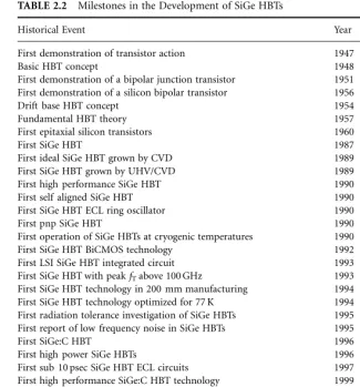
1947, at about 5 p.m. Not to be outdone, Shockley rapidly developed a theoretical basis for explaining how this clever object worked, and went on to demonstrate the first true bipolar junction transistor (BJT) in 1951 [27]. The first BJT was made, ironically in the present context, from Ge. The first silicon BJT was made by Teal in 1954 using grown junction techniques. The first diffused silicon BJT was demonstrated in 1956 [28], and the first epitaxially grown silicon BJT was reported in 1960, see Ref. [2]. The concept of the HBT is surprisingly an old one, dating in fact to the fundamental BJT patents filed by Shockley in 1948 [29]. Given that the first bipolar transistor was built from Ge, and III V semiconductors were not yet on the scene, it seems clear that Shockley envisioned the combination of Si (wide bandgap emitter) and Ge (narrow bandgap base) to form a SiGe HBT. The basic formulation and operational theory of the HBT, for both the traditional wide bandgap emitter plus narrow bandgap base approach found in most III V HBTs, as well as the drift base (graded) approach used in SiGe HBTs today, was pioneered by Kroemer, and was largely in place by 1957 [30 32]. It is ironic that Kroemer in fact worked hard early on to realize a SiGe HBT, without success, ultimately pushing him toward the III V material systems for his heterostructure studies, a path that proved in the end to be quite fruitful for him, since he shared the Nobel Prize in physics in 2000 for his work in (III V) bandgap engineering for electronic and photonic applications [33]. While III V HBT (e.g., AlGaAs GaAs) demonstrations began appearing in the 1970s, driven largely by the needs for active microwave components in the defense industry, reducing the SiGe HBT to practical reality took 30 years after the basic theory was in place due to material growth limitations. As pointed out [34] the semiconductor device field is quite unique in the scope of human history because ‘‘science’’ (theoretical understanding) preceded the ‘‘art’’ (engineering and subsequent technological advancement). Once device quality SiGe films were finally achieved in the mid 1980s, however, progress was quite rapid. Table 2.2 summarizes the key steps in the evolution of SiGe HBTs.
The first functional SiGe HBT was demonstrated by an IBM team in December 1987 at the IEDM [35]. The pioneering result showed a SiGe HBT with functional, albeit leaky, dc characteristics; but it was a SiGe HBT, it worked (barely), and it was the first.*It is an often overlooked historical point, however, that at least four independent groups were simultaneously racing to demonstrate the first functional SiGe HBT, all using the MBE growth technique: the IBM team [35], a Japanese team [62], a Bell Laboratories team [63], and a Linko¨ping University team [64]. The IBM team is fairly credited with the victory, since it presented (and published) its results in early December of 1987 at the IEDM (it would have been submitted to the conference for review in the summer 1987) [35]. Even for the published journal articles, the IBM team was the first to submit its paper for review (on November 17, 1987) [65]. All four papers appeared in print in the spring of 1988. Other groups soon followed with more SiGe HBT demonstrations.
The first SiGe HBT demonstrated using (the ultimately more manufacturable) CVD growth technique followed shortly thereafter, in 1989, first using LRP CVD [17], and then with UHV/CVD [36]. Worldwide attention became squarely focused on SiGe technology, however, in June 1990 at the IEEE VLSI Technology Symposium with the demonstration of a non self aligned UHV/CVD SiGe HBT with a peak cutoff frequency of 75 GHz [37,38]. At that time, this SiGe HBT result was roughly twice the performance of state of the art Si BJTs, and clearly demonstrated the future performance potential of the technology (doubling of transistor performance is a rare enough event that it does not escape significant attention!). Eyebrows were raised, and work to develop SiGe HBTs for practical circuit applications began in earnest in a large number of industrial and university laboratories around the world.y
The feasibility of implementing pnp SiGe HBTs was also demonstrated in June 1990 [40]. In December 1990, the simplest digital circuit, an emitter coupled logic (ECL) ring oscillator, using
*An interesting historical perspective of early SiGe HBT development at IBM is contained in Ref. [61].
yA variety of zero Dt, mesa isolated, III V like high speed SiGe HBTs were reported in the early 1990s (e.g., Ref.