Design Automation
for Diff erential MOS
Current-Mode Logic
Circuits
Stéphane Badel · Can Baltaci
Yusuf Leblebici
Design Automation for
Differential MOS
Current-Mode Logic Circuits
École Polytechnique Fédérale de Lausanne Lausanne, Switzerland
Alessandro Cevrero IBM Research – Zurich Rüschlikon, Switzerland
École Polytechnique Fédérale de Lausanne Lausanne, Switzerland
Yusuf Leblebici
École Polytechnique Fédérale de Lausanne Lausanne, Switzerland
ISBN 978-3-319-91306-3 ISBN 978-3-319-91307-0 (eBook)
https://doi.org/10.1007/978-3-319-91307-0
Library of Congress Control Number: 2018941809
© Springer International Publishing AG, part of Springer Nature 2019
This work is subject to copyright. All rights are reserved by the Publisher, whether the whole or part of the material is concerned, specifically the rights of translation, reprinting, reuse of illustrations, recitation, broadcasting, reproduction on microfilms or in any other physical way, and transmission or information storage and retrieval, electronic adaptation, computer software, or by similar or dissimilar methodology now known or hereafter developed.
The use of general descriptive names, registered names, trademarks, service marks, etc. in this publication does not imply, even in the absence of a specific statement, that such names are exempt from the relevant protective laws and regulations and therefore free for general use.
The publisher, the authors and the editors are safe to assume that the advice and information in this book are believed to be true and accurate at the date of publication. Neither the publisher nor the authors or the editors give a warranty, express or implied, with respect to the material contained herein or for any errors or omissions that may have been made. The publisher remains neutral with regard to jurisdictional claims in published maps and institutional affiliations.
Printed on acid-free paper
This Springer imprint is published by the registered company Springer International Publishing AG part of Springer Nature.
Our detailed research work on the design and optimization of high-performance MOS current mode logic (MCML) circuits at the Microelectronic Systems Lab-oratory (LSM) of EPFL started more than a decade ago. In the beginning, our main motivation was the reduction of power supply noise and substrate noise generated by high-speed logic units that have to operate in very close proximity to sensitive analog building blocks. While the fundamental concepts used in the design of MCML circuits were fairly well understood, relatively little work was available at that time to guide systematic analysis and especially design automation of such circuits. Our early research in this domain has led to the development of differential logic cell optimization techniques under arbitrary load conditions, as well as fully differential logic synthesis, and placement-and-routing (P&R) strategies that enable straightforward design automation of logic functions based on conventional hardware description languages such as VHDL and Verilog. Such logic units distinguish themselves with their capability of operating at multi-GHz frequencies while producing extremely low levels of supply noise. Nowadays, MCML-based circuit solutions are commonly used in various applications where high-performance operation is the primary objective.
In addition to high-speed operation, the fully differential nature of the MCML circuit style lends itself to implementation of logic blocks in which the power supply signature associated with the logic operations can be effectively suppressed. This property results in highly efficient implementation of various cryptographic functions with a remarkable immunity to differential power analysis (DPA) attacks. The fully differential current-mode operation principle of MCML circuits has also paved the way for the development of a completely new class of ultralow-power logic circuits called sub-threshold source-coupled logic (ST-SCL) which can achieve impressive energy efficiency operating with very low tail current levels (down to a few pA) while producing several hundreds of mV output voltage swing— a feature that is simply not possible in conventional CMOS logic circuits operating in sub-threshold regime. Our extensive work in this particular direction has already
been published in the form of a separate volume from Springer, entitledExtreme Low-Power Mixed Signal IC Design coauthored by A. Tajalli and Y. Leblebici (ISBN 978-1-4419-6477-9).
This volume covers systematic, in-depth analysis of MCML circuits in PartI
(Chaps. 2 and 3), followed by the principles of design automation for MCML in PartII(Chaps.4 and5), addressing fully differential logic synthesis, standard cell design, pin assignment, and placement-and-routing strategies. The last four chapters (PartIII) of the book are dedicated to specific design examples for high-speed design as well as cryptographic circuit applications, such as the DPA-resistant implementations of Grain-128 stream cipher and AES engines. The topics covered in this book would be beneficial to graduate students specializing in high-speed circuit design, as well as engineering professionals designing systems for high performance and DPA immunity.
The authors are truly indebted to many individuals who have contributed to this work. Our graduate students, as well as our colleagues, have consistently helped us with their generous assistance along the way. In particular, we acknowledge the valuable support provided over the years by Dr. Ilhan Hatirnaz, Dr. Francesco Regazzoni, Dr. Armin Tajalli, Ms. Tugba Demirci, and Mr. Michael Schwander. This work would not have been possible without their contributions.
Lausanne, Switzerland Stéphane Badel
Rüschlikon, Switzerland Alessandro Cevrero
Lausanne, Switzerland Yusuf Leblebici
14 May 2018
1 Introduction. . . 1
1.1 Noise in Integrated Circuits. . . 1
1.2 Low-Noise CMOS Logic Families. . . 2
1.3 MOS Current-Mode Logic. . . 3
1.4 Organization of the Book. . . 3
References. . . 3
Part I Analysis and Design of MOS Current-Mode Logic Circuits 2 Analysis of MOS Current-Mode Logic Circuits. . . 7
2.1 The EKV MOSFET Transistor Model. . . 7
2.1.1 Strong Inversion Regime. . . 7
2.1.2 Weak Inversion Regime. . . 8
2.1.3 Moderate Inversion Regime. . . 8
2.2 The MOS Differential Pair. . . 9
2.2.1 Strong Inversion Operation. . . 9
2.2.2 Subthreshold Operation. . . 12
2.2.3 Transregional Model. . . 13
2.3 Single-Level MCML Logic Gate. . . 16
2.3.1 Implementation of Load Devices. . . 17
2.3.2 DC Transfer Characteristic. . . 18
2.3.3 Noise Margin. . . 19
2.3.4 Logic Levels. . . 24
2.3.5 Dynamic Operation. . . 26
2.4 Multi-Level MCML Logic Gates. . . 30
2.4.1 DC Operation . . . 32
2.4.2 Common-Mode Input Level and Level Shifting. . . 35
2.4.3 Dynamic Operation. . . 38
2.5 Effect of Nonlinearities. . . 39
2.5.1 Load Devices. . . 40
2.5.2 Differential Pairs. . . 44
2.5.3 Junction Capacitances. . . 45
4.4.2 Cell Layout. . . 114
5.2.2 Bias Generator and Level Converters in the Synthesis Process. . . 121 6 Design Example I: Low-Noise Encoder Circuit for A/D Converter. . . 133
8.3 MCML Cell Library. . . 161
8.3.1 Library Parameters. . . 161
8.3.2 Cell Selection . . . 161
8.3.3 Cell Characteristics. . . 162
8.3.4 Cell Layout. . . 164
8.4 Implementation Results. . . 164
8.4.1 Comparison of MCML and CMOS. . . 164
References. . . 170
9 Design Example IV: Advanced Encryption Standard (AES). . . 171
9.1 Circuit Description. . . 171
9.2 MCML Cell Library. . . 172
9.2.1 Standard Cell Design with Power Gating. . . 172
9.2.2 Cell Selection . . . 174
9.2.3 Cell Characteristics. . . 174
9.3 Implementation Results. . . 177
References. . . 180
10 Conclusions. . . 181
10.1 Future Work. . . 182
Appendix A Large-Signal Transitional Model of the MOS Differential Pair. . . 183
Appendix B List of MCML Templates up to Three Levels. . . 187
Further Reading. . . 227
Introduction
Over the past decades, integrated circuits have evolved from circuits combining thousands of transistors to multi-billion devices in today’s advanced technologies. The continuous scaling of device dimensions in VLSI is enabling the integration of complete systems on a single die, which may include a combination of RF transceivers, analog processing, A/D and D/A conversion as well as complex digital functions and memory on a single chip.
Combining all these elements on a single chip has many advantages, including reduced cost, higher speed, and lower overall power dissipation. It does not come, however, without its very own problems, not the least of which is the increase in noise coupled from the digital functions to the analog parts.
1.1
Noise in Integrated Circuits
When sensitive analog parts are combined with complex digital blocks operating at very high switching frequencies, the noise generated by the digital parts is inevitably transmitted to the analog blocks, predominantly through the common substrate, resulting in a reduction of the dynamic range, or reduction of the accuracy of the analog circuits.
Noise in digital CMOS circuits is mainly generated by the rapid voltage variations caused by the switching of logic states, and the related up / charge-down currents. In a conventional CMOS logic gate, the rapid change of voltage in internal nodes is coupled to the substrate through junction or wiring capacitances, causing charges to be injected into the substrate. Eventually, these substrate currents cause voltage drops that can perturb analog circuits through capacitive coupling and through variation of the threshold voltage due to body effect [8,11].
Additionally, the high instantaneous currents needed to rapidly charge or dis-charge parasitic capacitances add up a large current spikes in the supply and ground
© Springer International Publishing AG, part of Springer Nature 2019 S. Badel et al.,Design Automation for Differential MOS Current-Mode Logic Circuits,https://doi.org/10.1007/978-3-319-91307-0_1
P+ N+ N+ P+ P+ N+
P− Substrate N− Well
VDD GND SIGNAL
Fig. 1.1 Schematic cross-section of a typical N-well CMOS process illustrating the different mechanisms of noise coupling between power and signal nets and the substrate
distribution networks, a phenomenon known an simultaneous switching noise (SSN). These current spikes cause voltage noise primarily through the inductance of off-chip bond-wires and on-chip power-supply rails. Ground supply networks are usually directly connected to the substrate, resulting in a direct coupling of the noise, and power networks are typically connected to very large N-well areas resulting in a consequently very large parasitic coupling capacitance to the substrate. Therefore, power and ground distribution networks are very noisy in CMOS circuits, and at the same time ideal mediums for the noise coupling to the substrate. Signal nets can also couple to the substrate, through diffusion and wiring capacitances, and signals with high energy and switching activity are thus critical from a noise perspective. This is the case especially for clock networks, which are the most active signals and dissipate large amounts of power (Fig.1.1).
1.2
Low-Noise CMOS Logic Families
Two effective techniques to reduce the noise generation in digital circuits are the reduction of the voltage swings, and the cancellation of transient currents during switching events. In the past few years, several new logic families have been proposed, that generate less noise than classical CMOS logic, and are thus suitable for integration in mixed-mode environment as a replacement or a complement of CMOS logic.
These new logic families can broadly be categorized into two classes:
• single-ended families, including Current Steering Logic (CSL) [9] and Current-Balanced Logic (CBL) [1], which are based on regular CMOS operation with the addition of a circuitry to limit or cancel the current transients,
• differential families, including Complementary Current Balanced Logic (C-CBL) [2], Folded Source-Coupled Logic (FSCL) [4], and MOS Current-Mode Logic (MCML) [12], where each transition is canceled by an equal and opposite complementary signal.
[2], traditional automation tools and design flows fail to accommodate many aspects associated with their differential nature. For this reason, large-scale implementation of digital circuits with low-noise differential logic families remains a difficult task, and few results have been reported yet.
Even for very specific targets such as the construction and routing of a fully differential clock distribution network, most of the design tasks have to be carried out manually—which inevitably limits the usability of differential techniques.
1.3
MOS Current-Mode Logic
MOS Current-Mode Logic (MCML) has been introduced in [12] as a new design style for high-speed logic circuit. The operation of MCML circuits is based on the principle of re-directing (or switching) the current of a constant current source through a fully differential network of input transistors, and utilizing the reduced-swing voltage drop on a pair of complementary load devices as the output. Therefore, MCML logic style simultaneously offers reduced voltage swings and differential operation, two key characteristics in reducing the generation of switching noise. In addition, MCML allows high-speed operation, and dissipates a constant power independently of the switching frequency.
Due to these advantageous characteristics, MCML gates have been implemented in various demanding applications such as high speed ring oscillators, frequency dividers, phase detectors, etc. [5–7, 10]. However, until now the design style has remained largely case-specific, where transistor sizing and biasing are chosen to satisfy the particular constraints of a demanding design specification, and standardization of components is not considered in a broader context.
1.4
Organization of the Book
This book addresses the practical aspects and issues related to the implementation of MCML-based logic circuits with a standard-cell methodology. The first part concentrates on the analysis and design of MCML circuits at the transistor-level. The second part focuses on higher-level aspects, including the design of standard-cell libraries and the design automation. The third part presents practical design examples with emphasis on low-noise and high-speed operation.
References
2. E.F.M. Albuquerque, M.M. Silva, Evaluation of substrate noise in CMOS and low-noise logic cells, in IEEE International Symposium on Circuits and Systems (ISCAS)(2001)
3. E.F.M. Albuquerque, M.M. Silva, A comparison by simulation and by measurement of the substrate noise generated by CMOS, CSL and CBL digital circuits. IEEE Trans. Circuits Syst. 52, 734–741 (2005)
4. D.J. Allstot, S.-H. Chee, S. Kiaei, M. Shrivastawa, Folded source-coupled logic vs. CMOS static logic for low-noise mixed-signal IC’s. IEEE Trans. Circuits Syst.40, 553–563 (1993) 5. H.T. Bui, Y. Savaria, 10 GHz PLL using active shunt-peaked MCML gates and improved
frequency acquisition XOR phase detector in 0.18μm CMOS, inIEEE International Workshop on System-on-Chip for Real-Time Applications(2004)
6. H.T. Bui, Y. Savaria, Shunt-peaking in MCML gates and its application in the design of a 20 Gb/s half-rate phase detector, in IEEE International Symposium on Circuits and Systems (ISCAS)(2004)
7. M.P. Houlgate, D.J. Olszewski, K. Abdelhalim, L. MacHeachern, Adaptable MOS current mode logic for use in a multiband RF prescaler, in IEEE International Symposium on Circuits and Systems (ISCAS)(2004)
8. S. Kiaei, D. Allstot, K. Hansen, N.K. Verghese, Noise considerations for mixed-signal RF IC transceivers. Wirel. Netw.4, 41–53 (1998)
9. H.-T. Ng, D.J. Allstot, CMOS current steering logic for low-voltage mixed-signal integrated circuits. IEEE Trans. Very Large Scale Integr. Syst.5, 301–308 (1997)
10. A. Tanabe, M. Umetani, I. Fujiwara, T. Ogura, K. Kataoka, M. Okihara, H. Sakuraba, T. Endoh, F. Masuoka, 0.18-μm CMOS 10-Gb/s multiplexer/demultiplexer ICs using current mode logic with tolerance to threshold voltage fluctuation. IEEE J. Solid State Circuits36, 988–996 (2001) 11. M. van Heijningen, J. Compiet, P. Wambacq, S. Donnay, M.G.E. Engels, and I. Bolsens, Analysis and experimental verification of digital substrate noise generation for epi-type substrates. IEEE J. Solid State Circuits35, 1002–1008 (2000)
Analysis of MOS Current-Mode Logic
Circuits
2.1
The EKV MOSFET Transistor Model
Throughout this chapter, we use a simple version of the EKV MOSFET transistor model [8]. The EKV model is a fully analytical, charge-based model and provides a simple yet accurate model for hand calculations, and a transregional modeling approach where the MOS transistor is first modeled in asymptotic modes, i.e. weak and strong inversion, and an analytical transregional expression is derived through a continuous interpolation function.
2.1.1
Strong Inversion Regime
In strong inversion, the drain current in the EKV model (without accounting for the body effect) is given in linear regime by
ID=n·β· V
G−VT
n −
VD+VS 2
·(VD−VS) (2.1)
whereVG,VS, andVDare the gate, source, and drain voltages, respectively,VT is the threshold voltage,nis the subthreshold slope parameter, andβ is the current factor defined as
β =μ· ǫox tox ·
W
L (2.2)
withμthe carrier mobility,ǫox andtox the dielectric constant and thickness of the gate dielectric, andW andLthe width and length of the gate. In saturation regime, whenn·VD> VG−VT, the drain current has the expression
© Springer International Publishing AG, part of Springer Nature 2019 S. Badel et al.,Design Automation for Differential MOS Current-Mode Logic Circuits,https://doi.org/10.1007/978-3-319-91307-0_2
ID=
The transconductance in strong inversion and saturation regime is given by
gm=
In weak inversion, the drain current in the EKV model (without accounting for the body effect) is given by
ID =IS·e
whereIS is the specific current given by
IS =2·n·β·UT2 (2.6)
andUT =k·T /qis the thermal voltage. In the saturation regime, i.e. whenVD ≫
VS, the expression reduces to
ID =IS·e
VG−VT−n·VS
n·UT (2.7)
The transconductance in weak inversion saturation is given by
gm=
In the moderate inversion regime, i.e. when the gate-to-source voltage is close to
VT, neither of the above expressions is accurate.
The interpolation can be done on the drain current or on the transconductance, with the second method preferred over the first. In the latest version of the EKV model, version 3.0 described in [6], the interpolation function is defined as
gm=
2.2
The MOS Differential Pair
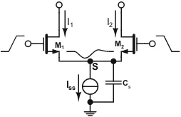
The MOS differential pair is the primary building block of MCML logic gates. Here, contrary to most analog applications where it is used in its linear operating region, the differential pair is used as an all-or-nothing, or binary, current switch. Just as the combination of MOS transistors used as voltage switches in CMOS or pass-transistor logic styles enables the realization of logic functions, logic functions are realized in MCML by combining current switches into specific networks.
Analytical models of the MOS differential pair will now be derived in strong and weak inversion. These well-known models are accurate enough for small-signal modeling, and prove useful for getting an insight into the operation of the differential pair. However they do not allow to model the differential pair over a wide range of current as required for the modeling of MCML circuits. Therefore a transregional model will be presented next that accurately models the large-signal behavior of the differential pair.
2.2.1
Strong Inversion Operation
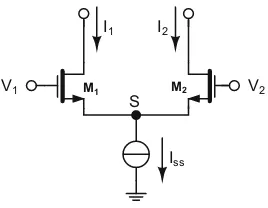
An MOS differential pair is depicted in Fig.2.1. It is composed of two identical MOS transistorsM1 andM2, with a common source connectionS. A current source keeps a constant currentISSflowing from theSnode, therefore the sum of the drain currents ofM1 andM2 is kept constant
I1+I2=ISS (2.10)
By summing the voltages around the loopV1−V2, we obtain a second equation
V1−V2=VG1−VG2 (2.11)
Substituting the expression of the gate voltage as given by the strong inversion EKV model into Eq. (2.11) yields the differential output current, using relation (2.10) then rearranging, we obtain
Vid = are identical. This expression can be inverted to give theΔI−Vidrelationship
ΔI
This relationship expresses the DC transfer curve for the circuit. It is important to notice that this equation relates the outputdifferentialcurrent to the inputdifferential voltage. The individual values ofV1andV2do not appear—only their difference. Similarly, a differential current is produced as output; the average current, or common-mode current, is defined by the tail currentISS.
Because the sum ofI1andI2must be equal toISS, it is clear that the maximum and minimum values ofΔIare limited to±ISS. This happens when the tail current is entirely switched onto one of the two transistors, and the other is turned off. The value ofVidneeded to accomplish this can be found by substitutingΔI = ±ISSin Eq. (2.13), yieldingVT s= ±
2nISS
β , whereVT sdenotes the switching threshold of the current switch.
The value ofVT sreflects the ability of the paired transistors to drive the current. The larger β, the smaller Vid needs to be to switch an equal amount of current. This value is linked to the transconductance of the transistors, which reflects their current driving ability. Let us define the differential transconductancegmd, defined as the small-signal increase in output current caused by an increase in input voltage
=
is the differential transconductance at equilibrium (Vid = 0), and is equal to the transconductance of a single transistor biased atID = ISS/2. Rewriting (2.14) in terms ofgmd,0, we obtain
The influence of transistor parameters is now explicit: their transconductance directly defines the slope of theΔI−Vidcurve and the whole transfer characteristic. It is therefore very practical, to normalizeVidtogmd,0/ISS−1andΔItoISS, as it is done in Fig.2.2which displays a plot of expression (2.16).
−1.5 −1.0 −0.5 0.0 0.5 1.0 1.5
2.2.2
Subthreshold Operation
As we have seen previously, the gain in the differential pair is proportional to the transconductance of the transistors biased at ISS/2. As we increase the transistor sizes in order to increase the gain, they will eventually enter subthreshold regime. When both transistors are in subthreshold regime, their drain currents grow exponentially with the gate-to-source voltage, according to the EKV model
ID=ISe
The equation can be reversed to express ΔII
SS, yielding
In this regime, the transconductance has a different expression
gmd=
gmd,0 cosh2 Vid
2nUT
wheregmd,0 = ISS/ (2·nUT)is the differential transconductance at equilibrium, and is here also equal to the transconductance of a single transistor biased atISS/2. Therefore, (2.17) can be normalized as
ΔI
−2.0 −1.5 −1.0 −0.5 0.0 0.5 1.0 1.5 2.0 Vid·(gmd,0/ISS)
−1.0 −0.5 0.0 0.5 1.0
∆
I
/
Iss
Fig. 2.3 Transfer curve of the differential pair in subthreshold regime
2.2.3
Transregional Model
So far, we have presented models of the differential pair both in strong and weak inversion. Both models give simple expressions to predict the shape of the transfer characteristic, which is a desirable property. However, they are both based on the strong assumption that both transistors operate in the same regime, and this assumption can only hold over a limited range.
In most of the cases, the large-signal operation of the differential pair cannot be analyzed accurately by considering a single mode of operation for the transistors— the exception being when it is operated in deep weak-inversion, over a range of currents where the subthreshold exponentialID−VGrelationship holds with good accuracy. When biased in strong (or moderate) inversion, the strong-inversion model will remain valid only as long as the gate-to-source voltages of both transistors remain large enough compared toVT, or equivalently as long as the current remains high enough in both branches. This is the reason why a strong-inversion model can correctly predict the behavior of the differential pair in the central region of the transfer characteristic, which is close to linear, but fails to accurately model the regions where the curve is bending.
0.0 0.5 1.0 1.5 2.0
Fig. 2.4 Transfer curve of a differential pair in 90 nm CMOS at different current levels and the ideal strong- and weak-inversion models (L=Lmin, W=5×L)
regime, however as Vid is increased, the real characteristics deviate from the expected ones and neither model offers acceptable accuracy. The actual value ofΔI
lies somewhere between the strong inversion and the weak inversion expressions. In order to model the large-signal behavior of the differential pair over a wide range of input voltages, we can adopt the interpolation approach of the EKV model. However, the interpolation function (2.9) is too complex to yield tractable expressions for hand analysis. Therefore, we will use the simpler expression
gm(ID)=
gsgw
gs +gw
(2.18)
where gs and gw are the expressions of the transconductance in strong and weak inversion, respectively. This interpolation is valid under the assumptions that
gw/gs → ∞whenID → ∞, andgw/gs → 0 when ID → 0, which hold for MOSFETs. This is graphically represented in Fig.2.5.
Then, sincegm=dID/dVG, we can obtainVGby integrating 1/gmas follows:
10−2 10−1 100 101 102 103
Fig. 2.5 Continuous interpolation of the transconductance from weak to strong inversion accord-ing to (2.18)
Vid =VG(I1)−VG(I2) =
VG(st rong)(I1)−VG(st rong)(I2)+VG(weak)(I1)−VG(weak)(I2)
=Vid(st rong)(ΔI )+Vid(weak)(ΔI ) (2.20)
where Vid(st rong) and Vid(weak) are theVid −ΔI transfer curves for the differ-ential pair in strong and weak inversion, respectively. Inserting (2.16) and (2.17) into (2.20) and rearranging, we obtain
Vid
where the quantity ISS/(2IS)in this expression is equal to the inversion factor at ID = ISS/2 as defined in the EKV model. The small-signal differential transconductance at equilibrium is given by
gmd,0=
Note that the maximum transconductance is equal to the value in weak inversion, i.e.ISS/(2nUT).
0.0 0.5 1.0 1.5 2.0 Vid·(gmd,0/ISS)
0.00 0.25 0.50 0.75 1.00
∆
I
/
Iss
ISS= 1µA ISS= 10µA ISS= 100µA
Fig. 2.6 Transfer curve of a differential pair in 90 nm CMOS at different current levels and the transregional model (L=Lmin, W=5×L)
by simulation in a 90 nm CMOS process. For each current level, the differential transconductancegmd,0has been extracted from the simulated data, by measuring the slope of the transfer curve in the linear region, and the resulting value used to calculate theISparameter in order to construct the analytical curves.
2.3
Single-Level MCML Logic Gate
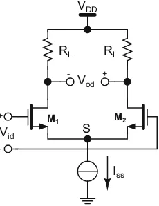
Fig. 2.7 MOS current-mode logic inverter/buffer
RL
Vid S
VDD
Vod
Iss
M1 M2
RL
+
-+
-2.3.1
Implementation of Load Devices
Practically, the pull-up devices in an MCML gate can be implemented either as passive or active devices. In the first case, various flavors exist in modern VLSI technologies:
• diffused resistors are implemented by the parasitic resistance of low-doped silicon. Depending on the doping, they can offer sheet resistances as high as 1 k/square, however they suffer from high parasitic capacitance due to the reverse biased pn-junction.
• polysilicon resistors are implemented with unsalicided strips of polysilicon. Typi-cally, polysilicon resistors offer sheet resistances in the range 200–500/square, and up to 1 k/square in processes offering high-resistive polysilicon. This type of resistance is more linear than diffused resistors and suffers less parasitic capacitance.
Passive resistors are inherently subject to process variations, due to doping, lithography, and etching. The tolerance on the absolute value of passive devices is typically as large as 20–30% of the nominal value.
Active resistors can be implemented with MOS devices operating in the linear region. They can offer an acceptable linearity if theirVGS is high and the voltage swing is small. Active resistors are naturally adjustable, by varying the bias voltage, so on-chip biasing can be implemented to compensate the process variations, and obtain very precise absolute values. Typical values for such passive resistors are in the range of 10–50 k/square of channel dimensions (Fig.2.8).
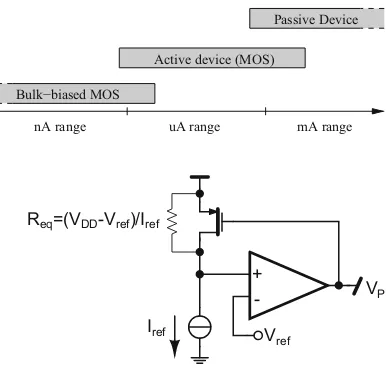
For very low current levels, active resistors with bulk biasing can be implemented to increase the resistivity, allowing up to several hundred of M/square. This technique is explained in detail in [17,18], and can be used for circuits biased in weak inversion, with very low current levels.
Fig. 2.8 Resistor devices and
sizes, while for low resistance values their dimensions and parasitics make them more efficient than active devices. Adjustment of the total resistance with passive devices can be achieved by circuit techniques, for example by combining active and passive devices in parallel, resulting in smaller overall dimensions than the use of an active device (Fig.2.9).
In this work, we are focusing on MCML design with application to standard-cell type of circuits, which implies that the device sizes that we are considering are in the range of the technology minimum, and that the devices should be biased in strong or moderate inversion to allow high speed operation. For this type of application, active loads offer the best compromise, and in the remaining of this text we will assume that load devices are realized with PMOS transistors biased in the linear region, unless explicitly stated otherwise.
2.3.2
DC Transfer Characteristic
In order to obtain an accurate large-signal model for theVod−Vidrelationship of the circuit in Fig.2.7, we use the transregional model proposed in the previous sections for the transfer function of the differential pair.
Derivation The differential voltageVod at the output of this circuit is given by
Vod =(VDD−RLI2)−(VDD−RLI1)
=RL(I1−I2)=RLΔI (2.23)
Vid
where thevoltage swingVsw=RLISSis equal to the maximum voltage drop across the individual load resistors (when±ΔI = ISS). For this circuit, thesmall-signal differential voltage gainis given by
Avd=gmd,0·RL=
using (2.22). This quantity can conveniently be substituted in the various expres-sions, with the desirable property of being directly measurable on the VTC as the slope at the origin. However, it encapsulates a dependency onVsw,ISS, andβwhich we regard as a fundamental design parameters. It is preferable when dealing with design problems to reason in terms of these parameters, that can be directly adjusted on the circuit and thus provide more useful insight into the tradeoffs. Therefore, we will exchangeably formulate the expressions in terms ofmeasurablequantities when a comparison is required with experimental data, and in terms ofadjustable parameters when discussing design decisions.
Approximation Expression (2.24) is a linear combination of two terms, corre-sponding, respectively, to the strong and weak inversion regimes. Because the weak inversion term accounts for most of the nonlinearity in the overall characteristic, the strong inversion term can be approximated by linearization with little loss of accuracy. This leads to the following simpler expression
Vid
Validation Expressions (2.24) and (2.26) are plotted in Fig.2.10 together with simulation results in a 90 nm CMOS technology. The simulation results are obtained with two different sizes for the transistors in the differential pair, atISS =10µA,
Vsw = 400 mV,T = 300 K and with pure resistive loads. In addition, the curves resulting from simple weak and strong inversion models are included, highlighting the benefits of using a transregional model.
2.3.3
Noise Margin
−4 −2 0 2 4
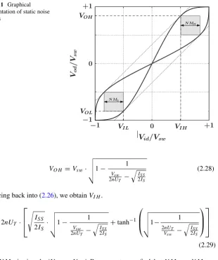
Fig. 2.10 Simulated transfer function of an MCML buffer in 90 nm CMOS technology, and the analytical model. Parameters are:VDD=1.2 V,ISS=10µA,Vsw=400 mV,T=300 K of a circuit is quite complicated, especially when considering a dynamic operation where the effect of noise is function of the duration and shape of the noise signals. For this reason, the most widely used criterion for quantifying noise robustness is the worst-case static noise margin. Worst-case static noise margins are evaluated by considering a quasi-static situation, where the duration of the noise is very long compared to the response time of the gates, and a worst case scenario where an equal amount of noise is applied at the input of each logic gate along an infinitely long chain. The noise margins are then defined as the maximum noise amplitude that does not perturb the logic state of the circuit.
As discussed in [10], the noise margin can be represented graphically by drawing the voltage transfer curve (VTC) of a gate, mirroring it along they = x line and drawing the maximum-sized square that fits in the area between the two curves (Fig.2.11). Furthermore, as pointed out in [11], theVI H,VOH,VI L, andVOLpoints as defined in the figure are the coordinates of the points where the derivative of the VTC is equal to one.
Derivation Differentiating (2.26) implicitly with respect toVod, we can express the derivative of the VTC for an MCML buffer as
∂Vid
Fig. 2.11 Graphical
N M
Expression (2.31) can be well approximated over the range of interest by the following formula
Validation Figure2.12plots the resulting expression against the values obtained by simulation using a 90 nm CMOS technology. As it can be seen, the analytical formula agrees well with the simulated data. It tends to slightly overestimate the noise margin when the pair is strongly inverted, i.e. for low values ofAvd and large values of Vsw, because of the linear approximation of the strong inversion characteristic. For larger values of Vsw, the transistors may enter linear region when their drain voltage is low—that is, whenVid is large—effectively reducing
1 2 3 4 5 6
their transconductance and thus flattening the transfer curve. This has the effect of reducing the noise margin, and is also not taken into account in the analysis.
Expression (2.33), also displayed in Fig.2.12, gives a very good approximation over a broad range of operating points. Several more simple expressions can be found, by considering only the weak or strong inversion behavior, however these expressions are poorly accurate, or accurate only within a limited range of operating points.
The weak-inversion limit is found by settingIS ≫ISSin the previous expression, yielding
Conversely, the noise margin considering only the strong-inversion behavior is found by settingIS ≪ISS, yielding
corresponding to a velocity saturation index [14,15] of α = 1, because this assumption was made to derive the initial formula (by linearizing the strong inversion characteristic). The expression for the case whereα = 2 can be found by following the same approach as previously, and was first calculated in [5] as
N Ms,2
As suggested in [2], this expression can be approximated by assumingVOH =
VswandAvd ≫1/
√
8, yielding a simpler formula
N Ms,3
or, by approximating even further
N Ms,4
1.0 1.5 2.0 2.5 3.0 3.5 4.0
Fig. 2.13 Comparison of different noise margin formulas. The symbols denote simulation results from Fig.2.12, at three differentVsw. The bold lines show the theoretical noise margin values from expression (2.30). The different thin lines show the resulting values from expressions (2.34)–(2.39)
N Mα
Vsw = 1− γ
Avd
(2.39)
whereγis a constant between 1 and√2, reflecting the effect of velocity saturation. In order to compare all these different expressions, verify their accuracy and assess their range of validity, they are all displayed on the same graph in Fig.2.13
together with the simulated data from Fig.2.12.
By inspecting the matching of the different curves to the simulated data in Fig.2.13, it appears that all approximations (2.34)–(2.39) suffer from an impor-tant degradation in accuracy, compared to expression (2.30). The weak-inversion approximation (2.34) is accurate at lower values ofVsw. Using the long-channel strong-inversion expression (2.36) is reasonable for small values ofAvd, however this expression is not simple enough to be used in calculations. For larger values (Avd>2) the approximations (2.38) and (2.39) are actually closer to the simulated data, but they have the undesirable drawback of altering the x-axis intercept at
Avd = 1. Those three expressions are nevertheless preferable over (2.35), (2.37) which are rather inaccurate.
2.3.4
Logic Levels
should be two such values for binary logic, one for each logic level, and these values are termed thestable logic levels, denotedVH andVL.
Derivation In the case of an MCML buffer with a transfer characteristic given by (2.24), symmetry implies that VH = −VL = VH L, and the logic levels must
Unfortunately, this transcendental equation cannot be solved analytically. How-ever, it can be reversed to obtain parameter values that result in a given logic level specification. DefiningVH L/Vsw =α, we can write
whereξ has the definition given in (2.32)
ξ = Vsw
Validation The relationship between the stable logic levels and the ξ value is plotted in Fig.2.14from simulations results in 90 nm CMOS technology at different voltage swings, ranging from 100 to 500 mV, and various device sizes for the transistors in the differential pair. On the same graph, the theoretical value as given by (2.42) is plotted with dotted lines.
Some important conclusions can be drawn from the inspection of this graph. Firstly, note that a given value ofξ corresponds to a unique value ofN M, as given by (2.31). Therefore, at a given noise margin, gates with a lower voltage swing exhibit better logic levels. This is easily understood when considering that, for lower voltage swings, a differential pair with larger transconductance (resulting in a larger voltage gain) need to be used in order to compensate for the loss in noise margin. Secondly, the graph shows that good logic levels cannot be obtained at very low voltage swings. In fact, for a given value ofVsw, there is a maximum value ofξ given by
ξmax=
Vsw 2nUT
1 2 3 4 5
Fig. 2.14 Stable logic levels in an MCML gate. Symbols denote simulation results in a 90 nm CMOS process, for voltage swings ranging from 100 to 500 mV; bold lines represent the theoretical value given in Eq. (2.42)
Vsw,min=2nUT ·
tanh−1(α)
α (2.43)
According to this result, the minimum allowable voltage swing to obtain a relative logic level of 99% is∼170 mV at room temperature, and rises to∼220 mV atT =
400 K. In practice, unlessISS is extremely low, the transistors need to be biased in moderate inversion in order to keep reasonable transistor sizes. This will further increase the minimum voltage swing to higher values.
2.3.5
Dynamic Operation
In order to achieve efficient design of MCML gates, it is important to understand their dynamic operation, that is, how they behave during switching events and how this behavior depends on their parameters. During the switching in an MCML gate, the two complementary outputs undergo an opposite change in voltage—one output being pulled low through the tail current of the differential pair while the second is pulled up to the supply voltage through the load resistor. Due to time constants in the system, these processes are not instantaneous and cause transition delay from input to output. But delay is not the only reason of analyzing the dynamic operation of a gate, for during the switching, multiple transient current paths can exist between supply and ground which may sum up as current spikes in the supply.
Fig. 2.15 Parasitic
by layout, the capacitance contributions are equal on both sides. The time constant at the output nodes is determined by the parasitics of the transistors (Cdb, the drain to bulk diffusion capacitance, andCgd, the gate-to-drain capacitance), the parasitics due to the pull-up load device denoted here byCP, and the external parasiticsCo andCc due to wiring and input capacitance of the driven gates. All together, and taking into account the Miller effect, the total load capacitance can be estimated as
Ct ot =2Cgd+Cdb+CP +Co+2CC
By writing Kirschoff’s current law at both output nodes, we obtain the following differential equations
Subtracting one from the other, the differential equation governing the output differential voltage is found as
τ ·dVod(t )
dt +Vod(t )−RLΔI (t )=0 (2.45)
whereτ is the time constant of the first-order system and is equal toτ =RLCt ot. After taking the Laplace transform and inverting, we get
Vod(s)=
RL·ΔI (s)
2.3.5.1 Step Response
The step response is found by considering that, during full switching, ΔI varies from−ISSto+ISSor vice versa. Therefore, usingΔI (s)=(±2ISS) /s, and taking the inverse Laplace transform, we find the step response as
Vod(t )−Vod(0)= ±2Vsw1−e−t /τ (2.47)
The propagation delay in this scenario is therefore equal to the well-known value for a first-order system
td=τ ·ln(2)≈0.69RLCt ot (2.48)
2.3.5.2 Ramp Response
A step input is only valid in limit case where the input signal is changing very fast compared to the output signal. In real situations, the input and input slopes are usually of the same order of magnitude, and the propagation delay depends on the shape of the input signal. To model this effect, we can approximate the input waveform as a linear ramp. Because the transfer characteristic of the differential pair is fairly linear over a broad range of input voltage, we can approximate it with a linear relationship as
−1 0 1 2 3 4 5
Fig. 2.16 Ramp response of an MCML buffer. Symbols denote simulation results with a 90 nm CMOS technology (ISS=30µA,AV =2)
By calculating the time point whereVod(t )−Vod(0) = Vsw, and subtracting
τi′/2, the expression for the delay is found. The resulting formula depends whether the output reaches the mid-point before or after the input saturates, which is function of the ratioτi/τ tends towardsτ. Thus, the delay increase due to a very slowly changing input is at the most of about 30%, which is rather low (Fig.2.17).
2.3.5.3 Power Supply Noise
10−1 100 101 102
τi/τ
0.5 0.6 0.7 0.8 0.9 1.0 1.1 1.2
td
/τ
Fig. 2.17 Propagation delay of an MCML buffer as a function of the input rise time. Symbols denote simulation results with a 90 nm CMOS technology
Isupply =ISS+CL d
dt [Vo1(t )+Vo2(t )] (2.52)
Therefore, power supply noise can result if the common-mode output voltage
Vcm = (Vo1+Vo2) /2 varies during the switching. By summing the differential equations forVo1andVo2as given by (2.44), then dividing by 2, we obtainVcmas
τ ·dVcm(t )
dt +Vcm(t )=VDD− Vsw
2
where bothRL·ΔI component have cancelled out. Obviously, the common mode is thus constant and equal to the supply voltage minus half of the voltage swing. Therefore, the generated supply noise is null; it is important to realize, though, that this is possible only because the transient components on both output nodes cancel each other perfectly, and that any asymmetry will invalidate this condition and result in switching noise.
2.4
Multi-Level MCML Logic Gates
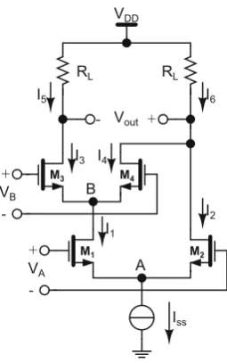
VA S
Fig. 2.18 (a) 2-Input AND/OR. (b) 2-to-1 multiplexer
a voltage drop at this node and effectively establishing the polarity of the differential output. Examples of logic networks are given in Fig.2.18a, b.
The logic network implemented in Fig.2.18a works as follows: when both inputs are in such a polarity that the differential pairs are steering current to their left branch, the current flows to the left output node, effectively pulling it low while the right output node is pulled high. In all other cases, the current is steered to the right output node. Polarities for inputs and output are intentionally not written on the picture, since all can be inverted at no cost, effectively realizing a logic inversion of an input or output: the same logic network will then be able to realize all possible variants obtained by inverting one or more of the inputs and/or output, without any change. Deciding on a polarity for inputs such thatM1andM3are conducting when
VA andVB are at the logic ‘1’ state, and for the output such that it is at logic ‘1’ state whenM5is pulling low, we can write the following truth-table
VA VB Vout
0 0 0
0 1 0
1 0 0
1 1 1
and therefore, the gate with the chosen polarities implements the 2-input AND function. By switching polarities of both inputs and the output, the 2-input OR function can be realized. All other combinations, including NAND and NOR, are also possible with the same gate.
D0=D1, the 2-input XOR function is obtained. Again, all combinations of input and output inversion are possible by simply switching the signal polarities.
The problem of determining what logic networks can be built and which functions can be realized will be one of the subjects of Chap.4, while in the following sections we will study the transistor-level operation of MCML logic networks.
2.4.1
DC Operation
Let us use as a case the 2-input AND network from Fig.2.19, with the defined currents and voltages. We consider the transfer function from each input to the output, in the case where the other input is constant. Furthermore, we will assume that each differential pair is working in the saturation region, so that they follow the transfer characteristic given by (2.24). For the constant inputs, we finally assume that the pairs behave as ideal current switches, switching only a fractionγ of their tail current, whereγ is related to the stable logic levels as defined in Sect.2.3.4
through
γ = 1+α
2 (2.53)
Considering input A, we assume thatVB is positive, so that I3 = α·I1 and
I2=(1−α)·I1. The output voltage is given by
Fig. 2.19 DC voltages and currents in the AND2 logic network
VA A
VDD
Vout
Iss
M1 M2
VB
M3 M4
+
-B
-+
- +
I2
I1
I3 I4
I6
I5
Vod =RL·(I5−I6) =RL·[I3−(I4+I2)]
=RL·[γ·I1−((1−γ )·I1+I2)] =RL·[2γ·I1−ISS]
Normalizing by dividing both sides byRL·ISS, we obtain
Vod
is the transfer function of the single differential pair as given by (2.21). We can make the following observations:
1. The transfer function is offset vertically by a factor(1+α)/2−1 2. The transfer function is scaled by a factor(1+α)/2
3. The logic levels are asymmetric
These effects are due to the imperfect current switching in theM3–M4 pair, and imply that the logic levels—and thus, the noise margin—are degraded in the multi-level gates when compared to a single-level gate with identical transistor dimensions.
When the transfer function is sufficiently flat at the crossing points, that is, for large enough values ofα, the logic levels approximately scale according to (2.54). SubstitutingΔI12=αresults in
α2≈(1+α)· 1+α
2 −1 (2.56)
0.80 0.85 0.90 0.95 1.00 α1
0.80 0.85 0.90 0.95 1.00
αN
N=1 N=2 N=3
Fig. 2.20 Logic level degradation in multi-level MCML gates. The plain lines represent for-mula (2.57) forN=1,2,3. The dotted lines denote simulation results obtained in a 90 nm CMOS technology, for AND gates with 1–3 inputs, withISS =100µA, at various voltage swings and
transistor sizes
Though this analysis is very simplistic, it allows to understand the effects involved. This is validated by the simulation results presented in Fig.2.20. In this figure, expression (2.57) is plotted in plain lines for a gate withN =1,2,3 levels of stacked differential pairs. The dotted lines represent simulation results, where the logic level corresponding to theN different inputs of each gate and four different values ofVsware all superimposed. The results show that, for large values ofα, the resulting logic level tends toward the curve given by (2.57).
The conclusion that can be drawn from these considerations is that, in order to design robust multi-level gates, the differential pairs should be able to efficiently switch the tail current. Moreover, with a higher number of levels, the current switching is less efficient and therefore the differential pairs should be sized larger. In practice, this implies that each additional level of stacked logic incurs additional costs in terms of area and speed.
2.4.2
Common-Mode Input Level and Level Shifting
In a multi-level MCML network, differential pairs that are located on the highest level have their drain connected to the output nodes and the load devices, and their source, when no switching is occurring on lower level inputs, is driven by a constant current. Therefore, they operate exactly as if they were single-level, and their characteristics are the same as that of a buffer as analyzed in the previous section.
The same is not true, however, for a pair located on a lower level. In the network of Fig.2.19, theM1transistor has its drain voltage equal to the source voltage of the
M3–M4differential pair. In a static condition, assuming that one ofM3orM4has a gate voltage ofVDDand is conducting all the current, the source voltageVB can be written asVB =(VDD−VT) /n−Vov(I1), whereVov is the overdrive voltage required to driveI1. Therefore, the condition forM1being saturated is written as
VDD−VT
n −Vov(I1)−
V1−VT
n ≥0
or
V1≤VDD−Vov(I1) (2.58)
Obviously, for this condition to remain true at all times, the input common mode-level of theM1–M2input pair must be lowered by an amount equal toVov(ISS). This can be achieved by inserting source–followers at the inputs as depicted in Fig.2.21a. In this configuration, both inputs V1 and V2 are shifted down by an amount equal to VT +Vov, depending on the size of the transistors in the level shifters and their tail current. Another option is to insert source followers at the output of the gates, as displayed in Fig.2.21b. The advantage of this configuration is that a single source–follower can provide a level-shifted signal to multiple gate inputs.
However, using level shifting has a number of important drawbacks:
V
inVDD V
DD
Vout,shifted V
a b DD
Vout
RL RL
• each source–follower stage creates an additional delay, of the same order of magnitude as the gate delay, thus resulting in a consequent speed penalty, • inserting the level-shifters at the input of the gate results in a very high number
of source–followers, resulting in a prohibitive cost in terms of area and power consumption
• inserting the level-shifters at the output of the gates is incompatible with an automated approach, since the load of each output (unshifted and shifted) cannot be determined a-priori, making it impossible to estimate the delay
• source–followers create an important amount of noise during switching
Not shifting the level of the input signals implies allowing the transistors in the differential pair to leave saturation region for a range of input voltages, as given in (2.58). Depending on the value ofVov, this range of voltage may be limited to a small range whenV1 ≈VDD, or extend so much as to keepM1from saturating most of the time.
One of the consequences of this is that, because the transconductance of the transistors in the differential pair is dependent on their drain voltage when they are not saturated, the transfer characteristic will become asymmetrical unless the drain voltages of both transistors are equal. In the case of the gate of Fig.2.19, the drain voltages ofM1andM2are very different, resulting in the transfer function displayed in Fig.2.22a, which plots simulation results for the AND2 network of Fig.2.19, together with the transfer function of a buffer with identical parameters. As it can be seen, the transfer curve of the asymmetrical network is shifted horizontally, resulting in an important decrease of the noise margin.
Though this decrease can be compensated by an increase in transistor sizes, the asymmetry of the network can also be compensated for, by balancing the network
−1.0 −0.5 0.0 0.5 1.0
as depicted on Fig. 2.22b, by adding transistor M7to lower the drain voltage of
M2to a value close to the drain voltage ofM1. In order to achieve balancing,M7 should have the same size asM3andM4, so that their gate-to-source voltage will be equal at equal drain current. The resulting transfer curve for the balanced network is also displayed in Fig.2.22a. In this example, the initial noise margin of 100 mV for the buffer drops to 35 mV for the asymmetrical network, while after balancing it restored to 60 mV.
There is another consequence of the transistors not being saturated: when the transistor leaves the saturation region, its transconductance drops—slowly in the beginning, and more sharply when entering deeper in the linear region. If the differential gain of the pair is larger than one when it enters linear region, the noise margin will be affected. This loss in noise margin can be compensated in two ways: by increasing the size of the transistors in theM1−M2 differential pair, and by reducing the overdrive voltage of the M3−M4 differential pair. In any case, it implies increasing transistor sizes, therefore reducing speed and increasing area.
In Fig.2.23, simulation results are displayed for a balanced AND2 logic network. These plots show the noise margin of the AND2 gate with respect to inputA, which drives the differential pair at the lower level of the network, as a function of transistor sizes. The effect of resizing theM1−M2andM3−M4pairs both independently and simultaneously is considered. As it can be seen, resizing a single pair has a limited effect on the noise margin, which increases with transistor size but quickly saturates. As the plots show, a good compromise is found when increasing both pairs simultaneously. This is confirmed by the simulation results in Fig.2.24, where the sizes of both differential pairs are swept, and the level curves at constant noise margin are extracted, together with a figure of merit for the area (A=2·W12+3·W34
Fig. 2.23 Noise margin compensation in an AND2 logic network without level shifting. The loss in noise margin is compensated by increasing transistor sizes ofM1−M2andM3−M4(−M7)
0.0 0.5 1.0 1.5 2.0 2.5 3.0
Fig. 2.24 Optimization of AND2 logic network transistor sizes. Simulations were performed with a 90 nm CMOS technology on the balanced AND2 network of Fig.2.22b
for the AND2 logic network). As predicted, the minimum area is consistently very close to the point whereW12=W34.
2.4.3
Dynamic Operation
The dynamic operation of multi-level MCML logic networks can be analyzed as it was done for the single-stage network in the previous section, by linearizing the differential pair transfer function.
Considering the balanced AND2 logic network of Fig.2.22b, let us first observe that, when inputB is switching, theM1−M2pair is largely unaffected and thus can be approximated by a constant current source. The dynamic behavior is thus exactly the same as for a single-stage network, except for additional parasitics due to increased transistor sizes, and additional connections to the output nodes. The same remains true for any logic network, when considering the switching of an input pair located on the top-most level of the network.
Fig. 2.25 Linear equivalent circuit of a two-level MCML logic network
Substituting (2.42), (2.32), and (2.53), this expression reduces to
ΔVS =
α
nVsw (2.60)
suggesting thatΔVS is close toVsw for practical values ofα. This provides a good approximation, therefore we will assume gms = 1/RL. Writing the differential equations for Vo1 and Vo2, and subtracting we get the differential equation for
Vod, and the linear equivalent circuit of Fig.2.25can be constructed. The transfer function for this circuit is found as
Vod most cases due to external load capacitance, the second-order system behavior can be approximated by a first-order system with a time constant equal to
τ =τL+τS =(CL+CS)
Vsw
ISS
(2.62)
The same analysis can be performed for logic networks withnlevels, yielding annth-order system, with a pole for each level. Therefore, the intrinsic propagation delay of a multi-level network will increase for each level of logic, starting from the top, by a constant factor. This is illustrated in Fig.2.26, where intrinsic delays are plotted for the different inputs of AND gates up to four levels.
2.5
Effect of Nonlinearities
Fig. 2.26 Simulated delays for multi-level logic networks. Simulations were carried in 90 nm CMOS technology with balanced
of the real-world devices is linear. Since nonlinearities will cause deviations from the ideal linear behaviors, it is interesting to examine their sources and their effects. Nonlinearities arise from various sources in integrated circuits in general; in MOS current-mode logic circuits in particular, there are three main sources: load devices, differential pairs and junction capacitances.
2.5.1
Load Devices
Ideally, load devices should be perfectly linear resistors. In practice, their linearity depends on their implementation: passive components, such as polysilicon resistors, can be highly linear; active devices, on the other hand, are inherently strongly nonlinear and the amount of nonlinearity greatly depends on the biasing and signal swings. In the previous discussions, the load devices have always been approximated by ideal linear resistors. Nonlinearity in the load devices will affect the DC characteristics as well as the transient behavior.
A PMOS device biased in the linear region obeys the followingI–V characteris-tic, as given by the EKV model
ID,lin =β·n·
0 Vsw VP
Fig. 2.27 Approximation of nonlinear load device
choose to equate both characteristics at both ends of the region of interest, that is, at
VDS =0 andVDS = −Vsw. With this definition, the equivalent resistance is given by
This definition allows to keep the Vsw parameter unchanged. Figure 2.27 illustrates the linear approximation of the load device; as it can be seen, the real resistance is always lower than the equivalent resistance over the region of interest. The real resistance value is given byR = |VDS/ID|, and the error in resistance due to the linear approximation is
ΔR(Vds)=Req−R
The average error over the region of interest is
Fig. 2.28 RC network with
Clearly, the error is an increasing function ofw. In order to minimize the error, the numerator can be decreased, or the denominator can be increased. In practice, this means using a smaller voltage swing, and using a gate voltage as low as possible, with a supply voltage as high as possible.
The consequences of nonlinearity in the load devices are twofold. First, because the actual resistance is always lower than the approximated linear value, the transfer characteristic of an MCML gate will be flattened, causing a decrease of the noise margin relative to the value calculated with linear load devices. Second, the nonlinearity will cause asymmetrical transient behavior at the rising and falling output nodes, which results in variation of the supply current during switching events. To understand this, let us calculate the step response of a RC network with nonlinear resistance, as shown in Fig.2.28, where the current through the resistance is voltage-dependent and expressed as
IR(Vo)=β·n·
Such a network obeys the differential equation
CL
0 1 2 3 4 5
Fig. 2.29 Supply noise caused by the nonlinearity of the load devices
Vo(f all)=VDD−VP
2.5.2
Differential Pairs
Differential pairs are inherently nonlinear. As for the nonlinearity in the load devices, the nonlinearity of the differential pairs will cause mismatches between the rising and falling behaviors during transitions, which sum up as current spikes. There are two types of switching events regarding the differential pairs: the switching of the differential input voltage, and the turning on and off of the tail current happening in multi-level logic networks.
The first type of switching event is illustrated in Fig.2.30: the gates of the transistors undergo an equal and opposite voltage variation. The study of the differential pair in steady-state conditions tells us that the sum of currents is always equal toISS, by Kirshoff’s law of currents at the source node. In transient conditions however, an additional current component goes to charge or discharge the capacitance at the source node. The sum of currents is therefore equal to
I1+I2=ISS+CS dVS
dt (2.71)
Note that, if the transistors behaved perfectly linearly with respect to their gate voltage, the source voltage VS would be constant during a transition. However, as it was shown earlier, the source voltage varies during transitions as given by formula (2.60). The variation of the source voltage can be written as
dVS
Therefore, the peak of current strongly depends on the rise time of the input signal. Essentially, this noise component will grow with the voltage swing, the capacitance at the nodeS(which consists of a constant part and a part proportional to transistor sizes, due to their source diffusion), and the speed of the input signal.
The second type of switching event in a differential pair is when the differential input voltage is constant and the tail current is switched on or off. This happens in gates with multiple levels of stacked differential pair, when a pair at a lower level is switching. Typically, such a switching event will involve simultaneously turning one pair on and another one off; because of the nonlinear behavior of the devices,
Fig. 2.31 Noise generation during the turning on/off of a differential pair tail current
the two current waveforms will not compensate each other and sum up as current spikes. This type of switching event is illustrated in Fig.2.31.
In this process, if we assume that the switching is instantaneous and reduce the transistor model to its strong inversion behavior, we can write the differential equation at nodeSas
ID =
The solution of this differential equation is different when the pair is turning on and when it is turning off,
ID(t )=
2 when turning OFF
ISS·tanh2
Clearly, the sum of those two currents cannot be null, and the resulting spikes depend on the value ofCShere also.
2.5.3
Junction Capacitances
whereVRis the (reverse) bias voltage across the junction,Vbiis the built-in voltage,
Cj0is the junction capacitance at zero bias, andmis an exponent depending on the doping profile. Typical values ofVbi are in the range of 0.5–1 V, and values ofm range from 1/3 to 1/2.
Note that the capacitance becomes more linear as the bias voltage increases. Since in MCML circuits the voltage swings are small and all nodes have a DC bias of at least several hundreds of millivolts, the effect of nonlinear junction capacitances is negligible for all practical purposes.
2.5.4
Overall Noise Performance
The different nonlinear effects that have been discussed separately are in practice all happening together, and affecting each other. It is hardly possible to predict accurately the result of simultaneous effects; some might tend to add up, while others might tend to cancel. It is thus interesting to construct an overall picture of the noise performance of MCML gates by simulations, with respect to the various design parameters.
Of all the contributions, the load device nonlinearity is probably the most important, because all other contributions depend on internal capacitances or time constants, and are filtered by the external load before reaching the supply. Since the load at the output nodes is typically much larger than at any internal node, all the internal current spikes tend to vanish at least partly in real situations. The spike of current due to the nonlinear loads, on the other hand, has a constant amplitude regardless of the switching speed of the output nodes.
Since as we have seen, the phenomena that cause the current spikes are transient, and depend on the signal rise times and shape, it is not meaningful to test a circuit in an ideal environment. In order to obtain pertinent results, a common test setup is to construct a ring oscillator out of the device to be tested. In this way, the device is functioning at a speed which is realistic, and all the signals in the circuit are real gate outputs and thus have a realistic shape.
200 250 300 350 400 450 500 550 600
Fig. 2.32 Supply noise in an MCML ring oscillator as a function of the design parameters. Simulation carried with 90 nm CMOS technology, atISS=100µA andN M=100 mV
2.6
Random Effects
Environmental variations will inevitably affect the operation of MCML circuits. These include variations in the device characteristics, due to process variations and mismatch, as well as operating supply voltage and temperature variations. MCML circuits are rather tolerant to environmental fluctuations since key performance parameters—speed and power dissipation of individual gates—are adjusted through bias voltages. An on-chip bias generation circuit should provide these voltages to ideally keep the voltage swing and tail current well-defined and constant. Though, strictly speaking, it is not necessary to use a bias generator, it is frequently used to counterbalance process variations.
Variations may appear at different levels, causing deviations from the expected characteristics:
• Process and environmental variations: variations affecting all devices equally. These variations include process variations due to the manufacturing, global supply voltage variations, and global temperature variations. In a closed loop approach involving a bias generator circuit, global variations are cancelled by adjusting the different parameters to the external references. However, these references may have a certain amount of uncertainty. In addition, imperfections in the bias generator (or absence thereof) will cause the adjusted parameters to vary.
causing the latter circuit to behave differently than the former. These include on-chip variations of the device parameters and local voltage drop in the power and ground distribution networks.
• Local mismatch:mismatch between two components assumed to be identical, within a single cell. This type of mismatch can affect the load devices and the differential pairs.
In the study of random effects, we are ultimately interested in determining the resulting variation in several parameters:
• Operating speed, in order to construct timing-correct circuits,
• Power dissipation, in order to determine the worst-case power consumption, and appropriately dimension power distribution networks, and
• Noise margin, which must remain positive in the worst-case.
2.6.1
Process Variations
Process variations, also called chip-to-chip variations, describe the fluctuation of the mean value of device characteristics. This kind of variation globally affects all devices on the chip.
As it has been stated, the use of a regulation circuit (bias generator) is frequent to cancel the process variations. In the absence of some form of regulation, it is hardly possible to keep the voltage swing under control, within a safe operating range.
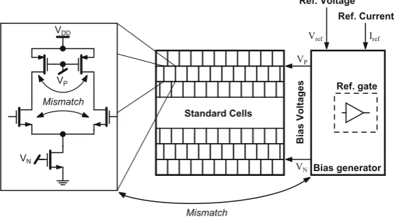
Typically, a replica scheme is used, as illustrated in Fig.2.33, where a circuit block receives bias voltages from an on-chip bias control block, which generates the bias voltages based on a reference voltage and a reference current. The bias
Bias generator Ref. Voltage
Ref. Current
Ref. gate
Bias Voltages
Standard Cells
VP
VN
VDD
VP
VN
Vref Iref
Mismatch
Mismatch