T here are probably hundreds of variations of capacitance sensors in use today, as any quick patent or literature search will quickly reveal. T he concept of charge sensing, on which all capacitance sensors are inherently based, goes back to work done in England in the 1740s by William Watson and shortly after in America by the scientist/statesman Benjamin F ranklin. By 1747, with the help of the newly available Leyden jar capacitor invented by G eorg von Kleist, both Watson and F ranklin had reached the conclusion that charge was a substance which, in an insulating system, is conserved. In 1752 F ranklin, in typically colorful Ameri-can style, conducted the first “natural” charge transfer experiments with a kite flown during a thunderstorm; the reproduction of this experiment eventually laid to rest arguments about the nature of lightning as well as a number of its researchers.
While the transference of charge is an essential aspect of every capacitance sensor, a relatively new form of sensor makes overt use of the principle of charge conservation first deduced by Watson in the 1740s. U pdated to use a microcontroller, mosfet switches, fet-input opamps and band gap references, the principle of charge transference can be used to create an extremely sensitive and stable device with unique properties that transcend those of more pedestrian capacitance sensors. Also known as “Q T ” sensors, charge transfer sensors can have a dynamic range spanning many decades with noise floors in the sub-femtofarad regime, allowing differential resolutions of mere fractions of a femtofarad. Such sensors are proving to have unique applications considered heretofore impossi-ble, while also proving themselves as replace-ments for much more expensive sensing systems using photoelectric, acoustic, RF, and optical imaging techniques.
Applications include human presence detection, fill level sensing, position sensing, material analysis, transducer drivers, keypads and touch controls, material imaging, and even in systems involving short range data transmission. Specific applications include in part intrusion and safety sensing, LVD T replacement, product moisture sensing, automatic water taps, in-keyboard “mouse” replacement, lighting controls, C apacitive
Sensor Review
Volume 19 · Number 2 · 1999 · pp. 96–105 M CB University Press · ISSN 0260-2288
Cha rge t ra nsf e r se nsing
H al Philipp
The author
Hal Philippis at Quantum Research Group Ltd, Enterprise House, Southampton, SO14 3XB. Tel: 01703 224 772; Fax: 01703 453 939; E-mail: [email protected]; WWW: w w w.qprox.com
Keyw ords
Capacitance, Sensors
Abstract
While the transference of charge is an essential aspect of every capacitance sensor, a relatively new form of sensor makes overt use of the principle of charge conservation first deduced by Watson in the 1740s. Updated to use a microcontroller, mosfet sw itches, fet-input opamps and band gap references, the principle of charge transference can be used to create an extremely sensitive and stable device w ith unique properties that transcend those of more pedestrian capacitance sensors. Also know n as “ QT” sensors, charge transfer sensors can have a dynamic range spanning many decades w ith noise floors in the sub-femtofarad regime, allow ing differential resolutions of mere fractions of a femtofarad. Such sensors are proving to have unique applications considered heretofore impos-sible, w hile also proving themselves as replacements for much more expensive sensing systems using photoelectric, acoustic, RF, and optical imaging techniques.
Electronic access
The research register for this journal is available at
ht t p://w w w 2.m cb.co.uk /m cbrr/sr.a sp
The current issue and full text archive of this journal is available at
ht t p://w w w .e m e ra ld-libra ry.com
Tomography (C T ) imaging, fruit ripeness testing, and even to help devise a new form of “smart card”. T he wide dynamic range and low cost of the Q T sensor permits application to a broad array of sensing problems, and opens up entirely new categories of potential applications.
How t he QT sensor w orks
T he QT sensor employs at its core the basic principles of physics explored by M essrs Watson and F ranklin; its implementation is essentially an engineering exercise in switching circuitry. By charging a sense electrode (which can be anything electrically conductive) to a fixed potential, then transferring that charge to a charge detector comprising another known capacitor, the capacitance of the sense electrode can be readily ascertained. T he charge and transfer operations are conducted by switches; while electromechanical switches would work quite well, in actual practice mosfet transistors are nearly ideal for the purpose. T he control of these mosfets is done by digital logic; in fact, the QT sensor is almost perfectly suited to digital control and processing. T he only analog signal is a typical-ly slow signal requiring no special precautions; conversion of this to digital can be performed by any of a number of commercially available analogue to digital converters.
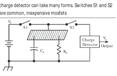
O ne form of Q T sensor used for ground-referenced or “open electrode” sensing involves the rapid charge and discharge of the sense element with respect to an earth return. An electrode element having a capacitance CX is first connected to a voltage reference via a switch S1 (F igure 1), S1 is reopened after CX is satisfactorily charged to the potential of the reference voltage VR. T hen, after as brief as possible a delay so as to minimize leakage effects caused by conductance RX(RXis inevitable in any system), switch S2 is closed and the charge QXpresent on CXis trans-ferred into the charge detector. O nce Qxis satisfactorily transferred, S2 is reopened; the charge is then read out of the charge detector and used. T he charge detector can simply be another capacitor, made much larger than the expected value of CX. As F igure 2 shows, a capacitor used as a charge detector must have a reset means (S3) to reset the charge between Q T cycles, so that each transfer cycle has a consistent initial condition. T he equations
which govern the sensor are the well estab-lished equations of charge transference:
(1)
If CXis much smaller than CS, then the equa-tion simplifies to:
(2)
T he value of capacitance can be ascertained by a slight rearrangement:
(3)
An improvement on this scheme is to simply repeat the Q T switching cycle many times before reading off V s and then resetting CSvia S3; manipulating the switches this way results in a system which provides intrinsic signal averaging, since CSacts as an integrator. T his scheme also increases usable gain, since every added Q T cycle adds more charge from the driven electrode. In one implementation, the system is run continuously, and S3 is replaced by a resistor (F igure 3). T he RS| CS combina-tion acts to produce a single-pole low-pass
C C V Figure 1 The simplified QT sensor circuit model. Sw itches S1 and S2 operate in time-sequence w ithout overlap. The charge detector can take many forms. Sw itches S1 and S2 are common, inexpensive mosfets
filter, and the “charge gain” (expressed as volts per farad) is determined by the values of RS, Vr, and the frequency at which the Q T switches are run. In contrast, a burst-mode Q T sensor’s gain is determined by Vr, CS, and the number of Q T cycles in each burst. An advantage of burst mode is that the gain can be readily controlled by numerically control-ling the burst length; this is not possible with continuous-Q T circuits such as that shown in F igure 3.
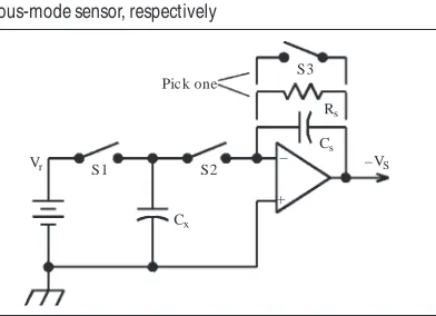
Another topology of Q T circuit is shown in F igure 4; here, the charge detector is actually an opamp, whose output drives negative as the charge is accumulated. A topology similar to that of F igure 2 is effected by using switch S3 across the opamp; a topology similar to that of F igure 3 is effected via the use the resistor RSas shown. T he advantage of using an opamp is that it creates a virtual ground into which CXis transferred, improving circuit linearity over a larger load range. T he disadvantage is the need for a negative power supply, a burdensome requirement in many low cost applications.
A topology which combines the linearity of the F igure 4 circuit with the single-supply simplicity of the F igure 2 circuit is shown in F igure 5. H ere, a controlled voltage source VZ is used to cancel the buildup of charge on CS by drawing charge out through CZas the charge is building on CS, in real time. Vzin practice is an opamp with a DAC driving it; during the course of a burst, the value of VZis lowered with each Q T cycle so that the charge transferred out of CSis nearly as much as that flowing into CSfrom CX. To accomplish this, VZmust first be set to some appropriately chosen positive voltage while S3 is closed, so that it can be lowered during the course of the burst. T he total output result is formed from the residual voltage left on CS, which is ampli-fied, plus the value of VZitself, which can be
iteratively determined; the value of VZ becomes a “coarse” signal approximation, while the residual on Csbecomes the
“vernier”. In many systems where only differ-ential capacitance is being monitored (e.g. motion sensing), the value of VZis ignored, while the amplified value of the residue on CS is used. VZthus is really being used merely to cancel background capacitances which may be due to cabling or to the physical size and location of the sense electrode itself. T he use of the VZcircuit extends the dynamic range of the sensor greatly.
T he total system gain of F igure 5 can be expressed as:
(4)
It is critical that the reference voltage Vrbe stable. Also, the amplifier should have suffi-cient stability and low input bias current.
V V C
C C n knC
S R X
S Z
X
= ⋅
+ ⋅ = ;
where n = QT cycles per burst.
Vr S1 S2 Vs
A
A x Vs
Cx Cs Rs
Figure 3 A continuous duty QT sensor model w ith sampler configured as a low -pass filter. Gain is a function of the reference voltage VR, operating frequency f and resistor Rs
Pick one
Vr S1 S2
Cx
S3
Rs Cs
–VS –
+
Figure 4 Model circuit having an opamp integrator as a Q sampler; topologies similar to those of Figures 2 and 3 are implemented by means of either a switch or resistor across the opamp to implement either a burst-mode or continu-ous-mode sensor, respectively
Control
S1 S2
Vs Vr
Cx Cs S3 Cz
Vz +
M odern fet-input opamps are ideally suited to this application.
N ote that the system gain is easily alterable by simply changing the number of transfer pulses within a burst. U nder microprocessor control, this is very easy to arrange. A micro-processor can also facilitate the incorporation of digital filtering, detection algorithms, and long term drift compensation.
Dynam ic range and sensing st abilit y In any real-world sensor application it is usually desirous to suppress background levels of CX, while being able to detect, with appropriate sensitivity, changes in CX, i.e.
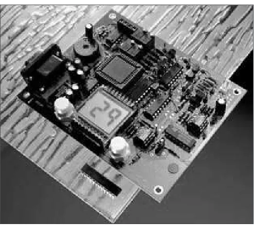
∆CX. For example, the use of a remote sense electrode connected to the sensor circuit via a 50 ohm coaxial cable will introduce about 100pF /meter of capacitance in parallel with the signal to be measured. F urthermore, the actual length of cabling will vary widely from system to system, placing a stiff requirement on the adaptability of a suitable commercial sensor. Tuned-circuit, bridge, and RC time-constant based capacitance sensors have enormous difficulties coping with wide varia-tions in large amounts of background C auto-matically. By using variable charge cancella-tion at the front end, a Q T sensor can accom-modate a broad sensing range in one circuit, while still providing a high level of differential sensitivity without placing a great demand on the analog path or on an AD C . For example, it is not a great feat to design a Q T circuit having a 5 femtofarad resolution while simul-taneously tolerating anywhere from 0 to over 300 picofarads of background load; such sensors are now commercially available from Q uantum Research G roup Ltd (F igure 6), who also offer embeddable Q T IC s and mod-ules. O ne such integrated circuit is the Q T 110 which costs as little as $1.95 (10k pcs) and is a fully self-calibrating Q T sensor for touch applications. It is designed to replace electro-mechanical switches. It also drives a piezo beeper and LED directly, and runs on com-mon lithium batteries for up to 15 years.
T he QT sensor does not employ many active components in its front end. In fact it could be argued that the mosfet switches S1 and S2 are for all intents passive, since they cannot introduce nonlinearities into the charge path (provided they remain closed long enough for sufficient charge to transfer); the remaining analog circuitry is composed of
ordinary D C coupled opamps. T his overt simplicity means the QT sensor can span many decades of range and maintain tremendous linearity throughout; the resolution, accuracy, and drift can be made as good as modern opamp and AD C technology will allow.
Susceptibility to external RFI is minimized by operating the transfer switches with short transfer times. D uring S1’s closure, the sense electrode is forcibly held to a low impedance reference, minimizing the fluctuations that an external field can induce. Only after S1 opens and S2 closes can external fields “get inside” the signal path; keeping S2’s operate time short helps to alleviate this problem. T his brevity reduces the “window of opportunity” for external fields to wreak havoc with the sensed signal. In contrast, RC based sensors have long exposures to external fields during their ramp times, while oscillator based circuits are contin-uously exposed to external fields.
Spread spect rum sensing
A significant advantage of burst mode Q T (“BQ T ”) sensors is the ability to provide a signal output in a repeatable amount of time, without having to wait for an asymptotic response to converge. T he BQ T sensor provides a repeatable and accurate result after each burst, which might last no more than a few microseconds. T he step response is characterized by a specified delay after which full output is guaranteed. T his delay time is
the same as the burst repetition spacing. T hus, if the burst spacing is 100 micro-seconds, the sensor is guaranteed to generate a 100 per cent accurate representation of a signal step within 100 microseconds.
A fascinating spread spectrum effect can be easily implemented by manipulating the pulse and/or burst spacings in a psuedo-random manner. T he introduction of timing random-ness causes spectral spreading akin to the frequency modulation of a carrier with broad-band noise. Again, this is an effect which most capacitance sensors would be hard pressed to emulate. O scillator based capacitance sensors have a monotonic and usually continuous fundamental; the fact that these circuits usually operate continuously means that their spectral power density is relatively high.
In contrast the BQ T sensor uses sparse pulses with long time gaps between bursts; total spectral power is therefore inherently weaker. A typical BQ T sensor operating with a 1ms burst spacing can have a total burst length of 50 microseconds containing 16 Q T switch cycles, for an effective “burst duty cycle” of 50/1,000 or 5 per cent. Since the individual transfer pulses can be very narrow, for example 5 per cent or less of the intra-burst pulse spacing, the integrated spectral energy of each burst is quite low to begin with, with actual spectral content appearing as a harmonic comb. Adding randomization to the pulse and burst spacing spreads the already weak fundamental and its harmonics around to even lower spectral densities.
Palpable advantages of the spread spec-trum mode include a marked desensitization to cross-sensor interference, reduced EM I problems, and reduced susceptibility to corre-lated noise. For a given power level at the sense element, the psuedo-random technique can greatly improve the odds of obtaining regulatory clearances for a given application.
Elect rode design f or charge t ransf er sensing
Sense electrodes are a critical part of any capacitive sensing solution. T here are three basic issues related to electrode size, shape, and placement:
(1) What can be made into a proximity sens-ing electrode?
(2) H ow sensitive will the sensor be? A corol-lary question is, “H ow far can it sense?” (3) What will the sense field shape be?
An excellent book which covers many of these topics is by Larry Baxter, Capacitive S ensors, Design and A pplications, IEEE Press (available from www.amazon.com), which covers elec-trode design in depth.
Intrinsic electrodes
M ost conducting objects can become an intrinsic electrode. While the object must not be directly grounded, Q Prox technology is particularly immune to partial conductance to ground when set to a short pulsewidth transfer time. Example conductances are from water films, or from the conductivity of electrode substrate materials such as wood (F igure 7).
Virtual electrodes
N on-conductive objects or conductive objects having an insulating layer can act as electrodes, so long as part of the surface is metallized or has a piece of metal attached, touching, or close by. A nonconductor that is made to act as a capacitive electrode can be thought of as a “virtual” electrode. Almost anything can be made into a virtual electrode; the effect works because objects and fluids have a much higher dielectric constant than air, and propagate the electric field quite well. T he resulting fields are weaker than had the object been made of metal, so the sense distance is less as well. H owever in many cases, such as with touch detection, this is not an issue.
Virtual electrode surfaces
A surface to which a metal electrode is attached can appear to exhibit a much larger “virtual” electrode surface (F igure 8). T he field will propagate laterally through the surface, effectively enlarging the sensitive surface area. T his effect will result in higher sensitivity than can be achieved with the metal electrode in free space alone, since capaci-tance is directly proportional to surface area.
T he degree of lateral spreading depends on the substrate thickness, composition, and nearness to grounded surfaces. T hick materials will tend to conduct the field through to the other side and spread the field thinly over a larger area, diluting the effect. Very thin materials will not be able to propagate the field laterally very far. Between these extremes are thicknesses which spread the field quite effectively. A grounded perimeter will help kill the field off beyond the confines of the grounding.
Electrodes for m aterial handling and fl uid fl ow
In material handling applications, shaped metal can be used to detect moving objects, obstructions, or flow or height of liquids, powders, or granules within vats, pipes, or along conveyors. Although capacitive fields are normally omnidirectional, the shape of the metal electrode and the use of nearby ground-ed metal can be usground-ed to tailor the sense field preferentially in certain directions (F igure 9).
For detecting the flow of materials in pipes, the pipe can have an isolated wire probe placed inside, or it can be partially lined with a thin layer of isolated metal. If the pipe is plastic or ceramic, the exterior of the pipe can have attached two metal foil electrodes (F igure 10). T he liquid’s high dielectric constant generates a strong signal. C onversely bubbles in the fluid are low dielectric regions that will create drops in the signal level; the QT sensor can thus be used to detect voids or bubbles.
Thin m aterial sensing
In films or webs, the material being sensed has little bulk and acts as a very weak target. U nless the web is partly conducting (for example a damp web of paper), the signal to be detected is challengingly small. O ne method of sensing the web is to use two paral-lel plates (one being earthed) with the materi-al running between them, thus amplifying the capacitive effect. T he plates must be mechani-cally very stable for this to work. Air gaps reduce the percentage change caused by the web material, so the spacing should be as close as possible.
If the material is conductive or wet, the sense electrode should have an insulating coating so that the material cannot short the electrodes together.
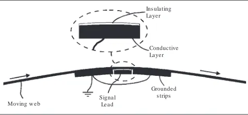
Another method of sensing a web is to use electrodes from only one side (F igure 11). T he web should be taut over the electrode set to ensure consistent contact. T he sense elec-trode should have an insulating cover layer (see reason above), and the gap between the electrodes should be comparable to or less than the material thickness. T he length of the electrodes across the width of the web will control the sensitivity. T his type of configura-tion can also be used to determine the Sens e Lead
VEW
EW
Figure 8 A virtual electrode surface is larger than the metal electrode w hich stimulates it. The virtual field can extend from both front and back of the substrate; the intensity of the field w ill exhibit a Gaussian rolloff beyond the metal electrode. Grounded strips w ill “ kill” most of the field beyond w here they are placed; such strips can be used to shape the field, for example to create an asymmet-ric field as show n
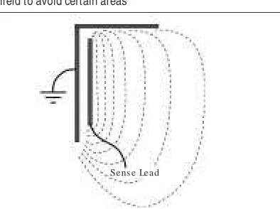
Sens e Lead
Figure 9 Grounded metal can be used to shape the sense field to avoid certain areas
moisture content of a moving web, at the same time as it checks for a web break.
M at erial analysis applicat ions
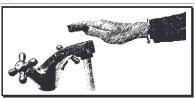
O riginally the author devised the BQ T sensor to suit a specific project: the development of a sensor to control an automated water tap (F igure 7), whereby the entire tap is made into a prox sensor. Aside from requiring that the tap be electrically isolated, an easy matter, the largest problem was avoiding the effects of water splashes around the base of the tap. As F igure 12 shows, a water film ionically conducts the sensing current through its length and breadth, effectively increasing the capacitive load in a random manner, wreaking havoc with detection algorithms. O n reflec-tion, it was realized that a water film acts electrically as a low-pass filter composed of a resistive sheet with parasitic capacitances to earth; such a “network” is highly frequency sensitive. At low sinusoidal frequencies, all parasitic capacitances attached to the sheet can be charged and discharged in unison, leading to a total value of CX that includes them all. At high frequencies, the network
“disconnects” the capacitances of the sheet since they are resistively coupled; the limited conductivity restricts the ability to charge and discharge the parasitic C s. T his effect results in a response curve with frequency as shown in F igure 13.
T his simple insight led the author to develop the BQT sensor, employing inexpensive pulse methods instead of expensive, power hungry C W oscillator based techniques of more conventional heritage. T he resulting tap sensor operates on battery power, and is currently in test at several plumbing companies in the U SA.
T he ability of the QT sensor to be “tuned” to suppress signals from a water film leads to a whole new realm of possible applications. As is well known, many insulating materials exhibit a frequency dependence in their properties such as dielectric constant and loss tangent; with some this dependence is negligible, however with a great many, especially organic compounds, this frequency dependence is significant. T he QT sensor can capitalize on this effect by observing corresponding signal variations in the time domain. By varying the transfer times on a given sample over a range, one can obtain a signal curve which is charac-teristic of the underlying material. T he shape or simply the slope of the cur ve at a particular point can be gainfully employed to deduce something about the material. A typical application of this might be to measure the moisture content of paper pulp, or to measure the ripeness of fruit. F igure 14 shows the example of the noninvasive capacitive response from two pears, one ripe and the other green; the curves are as obviously unique as can be. T he electrodes used to measure the data were simply two parallel metal strips measuring Ins ulating
Figure 11 A web can be sensed from one side, provided the gaps between the sense strip and ground strips are comparable to the material thickness, or less
Sens e Electrode Figure 12 An ionic film around the sense element, e.g. a water tap, causes a “ virtual spreading” of the capacitive electrode through the resistive water layer. The film’s response is highly frequency dependent, and in the time domain pulse w idth dependent
15mm by 3mm each and separated from each other longitudinally by a 0.5mm gap. Active work has now commenced in this area with citrus at the U niversity of F lorida using QT technology provided by Quantum Research. It can be envisioned that one day a hand-held sensor would be taken by a consumer to the grocery to help select more desirous fruits and vegetables, or that a wholesaler or grocer would use such a device to presort fruits to accommodate the customer.
T he method can potentially be used to determine the impurity content of fluids, for example water contamination of fuels, or to accurately gauge the phase transitions of various substances during processing. It could also be used to detect rain from within a car’s windscreen, for example, to control a “smart” wiper. It can also be used to drive transducers incorporating environmentally susceptible materials; for example, a hygroscopic material can be made into a detection film that
responds to humidity. T he number of applica-tions are seemingly endless. T he Q T sensor enables, for the first time in an economical form, the translation of reference book data on the frequency characteristics of materials into useful products.
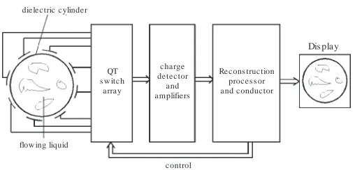
Capacit ive t om ography applicat ions Work done at the U niversity of M anchester and other universities on capacitive tomogra-phy has been ongoing since the early part of the decade. C apacitive C T work involves a variation on the Q T sensor described in this paper; the Q T sensor described so far is a single-ended system with an earth or chassis reference. C T technology requires the use of
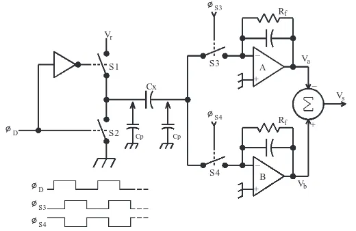
differential sensor methods to examine capac-itances among a number of electrodes radially positioned on the outer surface of a dielectric pipe (or inside a metallic pipe). C ross-capaci-tances among the various electrodes are used to reconstruct images of the contents of the pipe in real time (F igure 15). T he resulting images have been computed at frame rates up to 160/second and 32 ×32 pixel images, more than adequate to make respectable quantita-tive measurements on flowing materials at high speed. H igher pixel resolutions are obtainable at correspondingly higher cost. O ther materials aside from fluids can readily be examined as well. F igure 16(a) and (b) shows images of a flame within a cylindrical housing approximating an engine cylinder; six capacitive electrodes are positioned around its inner walls. F igure 17 shows how each sensing channel is implemented. A switched driver composed of S1 and S2 pulses one end of the differential capacitance CX, (which is any one of the permutations of capacitive couplings among the six electrodes around the pipe), while switches S3 and S4 are switched in quadrature with S1 and S2 respectively, pre-senting the opposite end of CXwith a virtual ground into which is captured an amount of charge QX= Vr×CX. Two lowpass filters provide an output for each edge transition; when the difference of these output voltages is taken, the value of CXcan be ascertained:
(6)
where f is the operating frequency, and e1 and e2 are error voltages from mismatched edge transitions, switch charge injection, and the like. T he errors largely cancel, while any residual error is subtracted algorithmically. T he result is an extremely stable, repeatable signal, resolvable enough to reconstruct
VS =VB–VA =2fV R Cr f X +e2–e1 QProx Fruit Ripeness Test
Puls ew idth, ns
0 200 400 600 800 1000
Figure 14 Similar to the response of a water film, a fruit’s response in the “ pulse domain” is highly dependent on its ripeness. A non-invasive, i.e. purely contacting instrument, can be devised to take advantage of this effect. Fruits are not the only objects having such response curves
dielectric cylinder
real-time images of great clarity with little additional filtering. A standard linear back projection algorithm is used to reconstruct images using an ordinary Pentium-class PC . Systems of up to 12 channels are currently being manufactured by Process Tomography Ltd.
A characteristic of this type of circuit is the ability to tolerate large amounts of parasitic capacitance Cpin the cabling and switches. Since this version of the Q T sensor employs differential sensing, capacitances to earth are effectively suppressed. D ifferential sensitivi-ties of 0.1 femtofarad have been achieved routinely for some time using such circuitry, while improvements are now permitting
resolutions approaching an almost unimagin-able 0.01 femtofarad.
Design considerat ions
An achilles heel of the Q T sensor when used with open sense elements is its need for a good quality ground reference in the local sensing environment, and low impedance connections to both ground and sense object. For self-contained sensing heads this is not a large concern, as the ground reference and sense plate are built into the sensor and are in close proximity to each other. H owever, for large freestanding electrodes the effects of rapid transfer currents should not be underes-timated. Poor, excessively inductive wiring with short S1/S2 closure times and high CX loads will create serious ringing and ground bounce problems which destroy transfer efficiency and linearity. T hese effects can be minimized by keeping connections short and of low inductance; they can also be minimized by simply using longer S1/S2 closure dura-tions. Adding a series-R to the sense lead will provide damping to stop ringing. With small, close-by objects ringing is not so much an issue; usually there is enough resistance in the switches, and voltage slew rates can be slowed enough to prevent observable problems. In any Q T sensor application however, the effects of connection quality should be fully evaluated and understood.
In designing a Q T circuit care should be taken to understand the nature of charge injection from the transfer switches. N ot all switches are equal, and few make good
(a) (b)
Figure 16 The capacitive tomography system can even image ionized gases, such as this propane flame. Other applications include the imaging of multiphase oil pipelines and fluidized beds
S1
S2 Cx
S3
Cp Cp
S4 B
A –
+
–
+ Rf
Rf Va
Vs
Vb Vr
∅S3
∅D
∅D
∅S3
∅S4
∅S4
–
choices. T hat being said, there are still a good number of suitable devices commercially available at reasonable cost. Parameters to look for are low output and reverse transfer capacitances, while maintaining suitably low on-resistances to allow sufficient settling time within the transfer duration. A poorly documented source of capacitance is the output capacitance due to the substrate diode found in nearly all mosfets. T his lack of documentation means that the designer must rely on vendor-supplied Spice models, or resort to “real-world simulation”, i.e. testing samples.
While it is tempting to use commercially available integrated analog switches for S1 and S2, the designer should be aware of the effects of control delay time. In many sensing systems a large time gap between the opening of S1 and closing of S2 is fatal; during such an interval leakage currents across CXcan drain CX’s charge, making the resulting signals noisy and unpredictable. M ost analog switches, even those purporting to be fast are fast only in the sense that they will have a wide signal bandpass, not have a fast turn-on or turn-off time. U sing mosfets as switches gives
the designer more control over transfer tim-ing, and is potentially less expensive as well.
T he designer should also be aware of refer-ence voltage stability issues. M ost series-pass voltage regulators do not have nearly enough transient stability to cope with the rapid trans-fer of charge into the sense electrode; load recovery times only prolong when using large supply bypass capacitors, often making the situation worse. Some of the newer IC pass regulators promise reference-diode stability, but the truth is that these too suffer from transient load recovery problems due to slow internal feedback paths. For the highest sensi-tivity Q T systems there is no substitute for a fast, high stability reference diode.
Conclusion