John Rogers
Calvin Plett
Artech House
Boston
•
London
Radio frequency integrated circuit design / John Rogers, Calvin Plett. p. cm. — (Artech House microwave library)
Includes bibliographical references and index. ISBN 1-58053-502-x (alk. paper)
1. Radio frequency integrated circuits—Design and construction. 2. Very high speed integrated circuits. I. Plett, Calvin. II. Title. III. Series.
TK7874.78.R64 2003
621.3845—dc21 2003041891
British Library Cataloguing in Publication Data Rogers, John
Radio frequency integrated circuit design. — (Artech House microwave library) 1. Radio circuits—Design and construction 2. Linear integrated circuits—Design and construction 3. Microwave integrated circuits—Design and construction
4. Bipolar integrated circuits—Design and construction I. Title II. Plett, Calvin 621.3’812
ISBN 1-58053-502-x
Cover design by Igor Valdman
2003 ARTECH HOUSE, INC. 685 Canton Street
Norwood, MA 02062
All rights reserved. Printed and bound in the United States of America. No part of this book may be reproduced or utilized in any form or by any means, electronic or mechanical, including photocopying, recording, or by any information storage and retrieval system, without permission in writing from the publisher.
All terms mentioned in this book that are known to be trademarks or service marks have been appropriately capitalized. Artech House cannot attest to the accuracy of this information. Use of a term in this book should not be regarded as affecting the validity of any trademark or service mark.
Foreword xv
Acknowledgments xix
1 Introduction to Communications Circuits 1
1.1 Introduction 1
1.2 Lower Frequency Analog Design and Microwave Design Versus Radio Frequency Integrated
Circuit Design 2
1.2.1 Impedance Levels for Microwave and
Low-Frequency Analog Design 2
1.2.2 Units for Microwave and Low-Frequency Analog
Design 3
1.3 Radio Frequency Integrated Circuits Used in a
Communications Transceiver 4
1.4 Overview 6
References 6
2 Issues in RFIC Design, Noise, Linearity, and
Filtering 9
2.1 Introduction 9
2.2 Noise 9
2.2.1 Thermal Noise 10
2.2.2 Available Noise Power 11
2.2.3 Available Power from Antenna 11
2.2.4 The Concept of Noise Figure 13
2.2.5 The Noise Figure of an Amplifier Circuit 14 2.2.6 The Noise Figure of Components in Series 16
2.3 Linearity and Distortion in RF Circuits 23
2.3.1 Power Series Expansion 23
2.3.2 Third-Order Intercept Point 27
2.3.3 Second-Order Intercept Point 29
2.3.4 The 1-dB Compression Point 30
2.3.5 Relationships Between 1-dB Compression and
IP3 Points 31
2.3.6 Broadband Measures of Linearity 32
2.4 Dynamic Range 35
2.5 Filtering Issues 37
2.5.1 Image Signals and Image Reject Filtering 37
2.5.2 Blockers and Blocker Filtering 39
References 41
Selected Bibliography 42
3 A Brief Review of Technology 43
3.1 Introduction 43
3.2 Bipolar Transistor Description 43
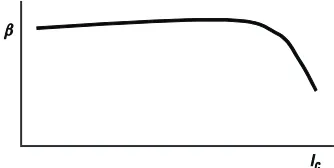
3.3 bCurrent Dependence 46
3.4 Small-Signal Model 47
3.5 Small-Signal Parameters 48
3.6 High-Frequency Effects 49
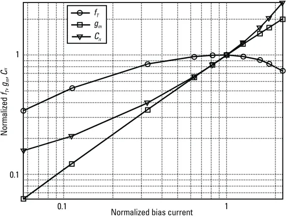
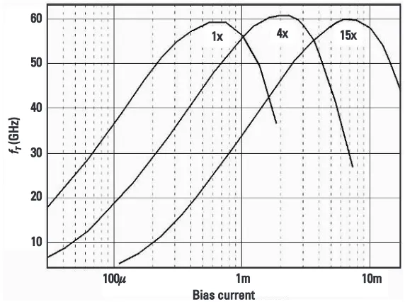
3.6.1 fTas a Function of Current 51
3.7 Noise in Bipolar Transistors 53
3.7.1 Thermal Noise in Transistor Components 53
3.7.2 Shot Noise 53
3.8 Base Shot Noise Discussion 55
3.9 Noise Sources in the Transistor Model 55
3.10 Bipolar Transistor Design Considerations 56
3.11 CMOS Transistors 57
3.11.1 NMOS 58
3.11.2 PMOS 58
3.11.3 CMOS Small-Signal Model Including Noise 58
3.11.4 CMOS Square Law Equations 60
References 61
4 Impedance Matching 63
4.1 Introduction 63
4.2 Review of the Smith Chart 66
4.3 Impedance Matching 69
4.4 Conversions Between Series and Parallel Resistor-Inductor and Resistor-Capacitor Circuits 74
4.5 Tapped Capacitors and Inductors 76
4.6 The Concept of Mutual Inductance 78
4.7 Matching Using Transformers 81
4.8 Tuning a Transformer 82
4.9 The Bandwidth of an Impedance Transformation
Network 83
4.10 Quality Factor of an LC Resonator 85
4.11 Transmission Lines 88
4.12 S,Y, and ZParameters 89
References 93
5 The Use and Design of Passive Circuit
Elements in IC Technologies 95
5.1 Introduction 95
5.2 The Technology Back End and Metallization in
5.3 Sheet Resistance and the Skin Effect 97
5.4 Parasitic Capacitance 100
5.5 Parasitic Inductance 101
5.6 Current Handling in Metal Lines 102
5.7 Poly Resistors and Diffusion Resistors 103
5.8 Metal-Insulator-Metal Capacitors and Poly
Capacitors 103
5.9 Applications of On-Chip Spiral Inductors and
Transformers 104
5.10 Design of Inductors and Transformers 106
5.11 Some Basic Lumped Models for Inductors 108
5.12 Calculating the Inductance of Spirals 110
5.13 Self-Resonance of Inductors 110
5.14 The Quality Factor of an Inductor 111
5.15 Characterization of an Inductor 115
5.16 Some Notes About the Proper Use of Inductors 117
5.17 Layout of Spiral Inductors 119
5.18 Isolating the Inductor 121
5.19 The Use of Slotted Ground Shields and
Inductors 122
5.20 Basic Transformer Layouts in IC Technologies 122
5.21 Multilevel Inductors 124
5.22 Characterizing Transformers for Use in ICs 127
5.23 On-Chip Transmission Lines 129
5.23.1 Effect of Transmission Line 130
5.23.2 Transmission Line Examples 131
5.24 High-Frequency Measurement of On-Chip Passives and Some Common De-Embedding
5.25 Packaging 135
5.25.1 Other Packaging Techniques 138
References 139
6 LNA Design 141
6.1 Introduction and Basic Amplifiers 141 6.1.1 Common-Emitter Amplifier (Driver) 141 6.1.2 Simplified Expressions for Widely Separated
Poles 146
6.1.3 The Common-Base Amplifier (Cascode) 146 6.1.4 The Common-Collector Amplifier (Emitter
Follower) 148
6.2 Amplifiers with Feedback 152
6.2.1 Common-Emitter with Series Feedback (Emitter
Degeneration) 152
6.2.2 The Common-Emitter with Shunt Feedback 154
6.3 Noise in Amplifiers 158
6.3.1 Input-Referred Noise Model of the Bipolar
Transistor 159
6.3.2 Noise Figure of the Common-Emitter Amplifier 161 6.3.3 Input Matching of LNAs for Low Noise 163 6.3.4 Relationship Between Noise Figure and Bias
Current 169
6.3.5 Effect of the Cascode on Noise Figure 170 6.3.6 Noise in the Common-Collector Amplifier 171
6.4 Linearity in Amplifiers 172
6.4.1 Exponential Nonlinearity in the Bipolar
Transistor 172
6.4.2 Nonlinearity in the Output Impedance of the
Bipolar Transistor 180
6.4.3 High-Frequency Nonlinearity in the Bipolar
Transistor 182
6.4.4 Linearity in Common-Collector Configuration 182
6.5 Differential Pair (Emitter-Coupled Pair) and
Other Differential Amplifiers 183
6.6 Low-Voltage Topologies for LNAs and the Use
6.7 DC Bias Networks 187
6.7.1 Temperature Effects 189
6.8 Broadband LNA Design Example 189
References 194
Selected Bibliography 195
7 Mixers 197
7.1 Introduction 197
7.2 Mixing with Nonlinearity 197
7.3 Basic Mixer Operation 198
7.4 Controlled Transconductance Mixer 198
7.5 Double-Balanced Mixer 200
7.6 Mixer with Switching of Upper Quad 202
7.6.1 Why LO Switching? 203
7.6.2 Picking the LO Level 204
7.6.3 Analysis of Switching Modulator 205
7.7 Mixer Noise 206
7.8 Linearity 215
7.8.1 Desired Nonlinearity 215
7.8.2 Undesired Nonlinearity 215
7.9 Improving Isolation 217
7.10 Image Reject and Single-Sideband Mixer 217 7.10.1 Alternative Single-Sideband Mixers 219
7.10.2 Generating 90°Phase Shift 220
7.10.3 Image Rejection with Amplitude and Phase
Mismatch 224
7.11 Alternative Mixer Designs 227
7.11.1 The Moore Mixer 228
7.11.2 Mixers with Transformer Input 228
7.11.3 Mixer with Simultaneous Noise and Power
Match 229
7.12 General Design Comments 231
7.12.1 Sizing Transistors 232
7.12.2 Increasing Gain 232
7.12.3 Increasing IP3 232
7.12.4 Improving Noise Figure 233
7.12.5 Effect of Bond Pads and the Package 233 7.12.6 Matching, Bias Resistors, and Gain 234
7.13 CMOS Mixers 242
References 244
Selected Bibliography 244
8 Voltage-Controlled Oscillators 245
8.1 Introduction 245
8.2 Specification of Oscillator Properties 245
8.3 The LC Resonator 247
8.4 Adding Negative Resistance Through Feedback
to the Resonator 248
8.5 Popular Implementations of Feedback to the
Resonator 250
8.6 Configuration of the Amplifier (Colpitts or
−Gm) 251
8.7 Analysis of an Oscillator as a Feedback System 252 8.7.1 Oscillator Closed-Loop Analysis 252 8.7.2 Capacitor Ratios with Colpitts Oscillators 255
8.7.3 Oscillator Open-Loop Analysis 258
8.7.4 Simplified Loop Gain Estimates 260
8.8 Negative Resistance Generated by the Amplifier 262 8.8.1 Negative Resistance of Colpitts Oscillator 262 8.8.2 Negative Resistance for Series and Parallel
Circuits 263
8.8.3 Negative Resistance Analysis of −Gm Oscillator 265
8.9 Comments on Oscillator Analysis 268
8.11 A Modified Common-Collector Colpitts
Oscillator with Buffering 270
8.12 Several Refinements to the −Gm Topology 270
8.13 The Effect of Parasitics on the Frequency of
Oscillation 274
8.14 Large-Signal Nonlinearity in the Transistor 275
8.15 Bias Shifting During Startup 277
8.16 Oscillator Amplitude 277
8.17 Phase Noise 283
8.17.1 Linear or Additive Phase Noise and Leeson’s
Formula 283
8.17.2 Some Additional Notes About Low-Frequency
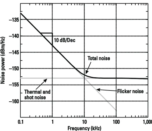
Noise 291
8.17.3 Nonlinear Noise 292
8.18 Making the Oscillator Tunable 295
8.19 VCO Automatic-Amplitude Control Circuits 302
8.20 Other Oscillators 313
References 316
Selected Bibliography 317
9 High-Frequency Filter Circuits 319
9.1 Introduction 319
9.2 Second-Order Filters 320
9.3 Integrated RF Filters 321
9.3.1 A Simple Bandpass LC Filter 321
9.3.2 A Simple Bandstop Filter 322
9.3.3 An Alternative Bandstop Filter 323
9.4 Achieving Filters with HigherQ 327
9.4.1 Differential Bandpass LNA withQ-Tuned Load
Resonator 327
9.4.2 A Bandstop Filter with Colpitts-Style Negative
Resistance 329
9.4.3 Bandstop Filter with Transformer-Coupled−Gm
9.5 Some Simple Image Rejection Formulas 333
9.6 Linearity of the Negative Resistance Circuits 336
9.7 Noise Added Due to the Filter Circuitry 337
9.8 AutomaticQ Tuning 339
9.9 Frequency Tuning 342
9.10 Higher-Order Filters 343
References 346
Selected Bibliography 347
10 Power Amplifiers 349
10.1 Introduction 349
10.2 Power Capability 350
10.3 Efficiency Calculations 350
10.4 Matching Considerations 351
10.4.1 Matching to S22* Versus Matching toGopt 352
10.5 Class A, B, and C Amplifiers 353
10.5.1 Class A, B, and C Analysis 356
10.5.2 Class B Push-Pull Arrangements 362
10.5.3 Models for Transconductance 363
10.6 Class D Amplifiers 367
10.7 Class E Amplifiers 368
10.7.1 Analysis of Class E Amplifier 370
10.7.2 Class E Equations 371
10.7.3 Class E Equations for Finite Output Q 372 10.7.4 Saturation Voltage and Resistance 373
10.7.5 Transition Time 373
10.8 Class F Amplifiers 375
10.8.1 Variation on Class F: Second-Harmonic Peaking 379 10.8.2 Variation on Class F: Quarter-Wave
Transmission Line 379
10.9 Class G and H Amplifiers 381
10.11 Summary of Amplifier Classes for RF Integrated
Circuits 384
10.12 AC Load Line 385
10.13 Matching to Achieve Desired Power 385
10.14 Transistor Saturation 388
10.15 Current Limits 388
10.16 Current Limits in Integrated Inductors 390
10.17 Power Combining 390
10.18 Thermal Runaway—Ballasting 392
10.19 Breakdown Voltage 393
10.20 Packaging 394
10.21 Effects and Implications of Nonlinearity 394
10.21.1 Cross Modulation 395
10.21.2 AM-to-PM Conversion 395
10.21.3 Spectral Regrowth 395
10.21.4 Linearization Techniques 396
10.21.5 Feedforward 396
10.21.6 Feedback 397
10.22 CMOS Power Amplifier Example 398
References 399
About the Authors 401
I enjoyed reading this book for a number of reasons. One reason is that it addresses high-speed analog design in the context of microwave issues. This is an advanced-level book, which should follow courses in basic circuits and transmission lines. Most analog integrated circuit designers in the past worked on applications at low enough frequency that microwave issues did not arise. As a consequence, they were adept at lumped parameter circuits and often not comfortable with circuits where waves travel in space. However, in order to design radio frequency (RF) communications integrated circuits (IC) in the gigahertz range, one must deal with transmission lines at chip interfaces and where interconnections on chip are far apart. Also, impedance matching is addressed, which is a topic that arises most often in microwave circuits. In my career, there has been a gap in comprehension between analog low-frequency designers and microwave designers. Often, similar issues were dealt with in two different languages. Although this book is more firmly based in lumped-element analog circuit design, it is nice to see that microwave knowledge is brought in where necessary.
Too many analog circuit books in the past have concentrated first on the circuit side rather than on basic theory behind their application in communica-tions. The circuits usually used have evolved through experience, without a satisfying intellectual theme in describing them. Why a given circuit works best can be subtle, and often these circuits are chosen only through experience. For this reason, I am happy that the book begins first with topics that require an intellectual approach—noise, linearity and filtering, and technology issues. I am particularly happy with how linearity is introduced (power series). In the rest of the book it is then shown, with specific circuits and numerical examples, how linearity and noise issues arise.
In the latter part of the book, the RF circuits analyzed are ones that experience has shown to be good ones. Concentration is on bipolar circuits, not metal oxide semiconductors (MOS). Bipolar still has many advantages at high frequency. The depth with which design issues are addressed would not be possible if similar MOS coverage was attempted. However, there might be room for a similar book, which concentrates on MOS.
In this book there is a lot of detailed academic exploration of some important high-frequency RF bipolar ICs. One might ask if this is important in design for application, and the answer is yes. To understand why, one must appreciate the central role of analog circuit simulators in the design of such circuits. At the beginning of my career (around 1955–1960) discrete circuits were large enough that good circuit topologies could be picked out by bread-boarding with the actual parts themselves. This worked fairly well with some analog circuits at audio frequencies, but failed completely in the progression to integrated circuits.
In high-speed IC design nowadays, the computer-based circuit simulator is crucial. Such simulation is important at four levels. The first level is the use of simplified models of the circuit elements (idealized transistors, capacitors, and inductors). The use of such models allows one to pick out good topologies and eliminate bad ones. This is not done well with just paper analysis because it will miss key factors, such as the complexities of the transistor, particularly nonlinearity and bias and signal interaction effects. Exploration of topologies with the aid of a circuit simulator is necessary. The simulator is useful for quick iteration of proposed circuits, with simplified models to show any fundamental problems with a proposed circuit. This brings out the influence of model parameters on circuit performance. This first level of simulation may be avoided if the best topology, known through experience, is picked at the start.
The second level of simulation is where the models are representative of the type of fabrication technology being used. However, we do not yet use specific numbers from the specific fabrication process and make an educated approximation to likely parasitic capacitances. Simulation at this level can be used to home in on good values for circuit parameters for a given topology before the final fabrication process is available. Before the simulation begins, detailed preliminary analysis at the level of this book is possible, and many parameters can be wisely chosen before simulation begins, greatly shortening the design process and the required number of iterations. Thus, the analysis should focus on topics that arise, given a typical fabrication process. I believe this has been done well here, and the authors, through scholarly work and real design experience, have chosen key circuits and topics.
estimates of parasitic capacitances from interconnections and detailed models of the elements used.
The incorporation of the proprietary models in the simulation of the circuit is necessary because when the IC is laid out in the actual process, fabrication of the result must be successful to the highest possible degree. This is because fabrication and testing is extremely expensive, and any failure can result in the necessity to change the design, requiring further fabrication and retesting, causing delay in getting the product to market.
The fourth design level is the comparison of the circuit behavior predicted from simulation with that of measurements of the actual circuit. Discrepancies must be explained. These may be from design errors or from inadequacies in the models, which are uncovered by the experimental result. These model inadequacies, when corrected, may result in further simulation, which causes the circuit design and layout to be refined with further fabrication.
This discussion has served to bring attention to the central role that computer simulation has in the design of integrated RF circuits, and the accompa-nying importance of circuit analysis such as presented in this book. Such detailed analysis may save money by facilitating the early success of applications. This book can be beneficial to designers, or by those less focused on specific design, for recognizing key constraints in the area, with faith justified, I believe, that the book is a correct picture of the reality of high-speed RF communications circuit design.
This book has evolved out of a number of documents including technical papers, course notes, and various theses. We decided that we would organize some of the research we and many others had been doing and turn it into a manuscript that would serve as a comprehensive text for engineers interested in learning about radio frequency integrated circuits (RFIC). We have focused mainly on bipolar technology in the text, but since many techniques in RFICs are indepen-dent of technology, we hope that designers working with other technologies will also find much of the text useful. We have tried very hard to identify and exterminate bugs and errors from the text. Undoubtedly there are still many remaining, so we ask you, the reader, for your understanding. Please feel free to contact us with your comments. We hope that these pages add to your understanding of the subject.
Nobody undertakes a project like this without support on a number of levels, and there are many people that we need to thank. Professors Miles Copeland and Garry Tarr provided technical guidance and editing. We would like to thank David Moore for his input and consultation on many aspects of RFIC design. David, we have tried to add some of your wisdom to these pages. Thanks also go to Dave Rahn and Steve Kovacic, who have both contributed to our research efforts in a variety of ways. We would like to thank Sandi Plett who tirelessly edited chapters, provided formatting, and helped beat the word processor into submission. She did more than anybody except the authors to make this project happen. We would also like to thank a number of graduate students, alumni, and colleagues who have helped us with our understanding of RFICs over the years. This list includes but is not limited to Neric Fong,
1
Introduction to Communications
Circuits
1.1 Introduction
Radio frequency integrated circuit(RFIC) design is an exciting area for research or product development. Technologies are constantly being improved, and as they are, circuits formerly implemented as discrete solutions can now be inte-grated onto a single chip. In addition to widely used applications such as cordless phones and cell phones, new applications continue to emerge. Examples of new products requiring RFICs arewireless local-area networks(WLAN), keyless entry for cars, wireless toll collection, Global Positioning System (GPS) navigation, remote tags, asset tracking, remote sensing, and tuners in cable modems. Thus, the market is expanding, and with each new application there are unique challenges for the designers to overcome. As a result, the field of RFIC design should have an abundance of products to keep designers entertained for years to come.
This huge increase in interest inradio frequency(RF) communications has resulted in an effort to provide components and complete systems on anintegrated circuit (IC). In academia, there has been much research aimed at putting a complete radio on one chip. Since complementary metal oxide semiconductor (CMOS) is required for the digital signal processing (DSP) in the back end, much of this effort has been devoted to designing radios using CMOS technolo-gies [1–3]. However, bipolar design continues to be the industry standard because it is a more developed technology and, in many cases, is better modeled. Major research is being done in this area as well. CMOS traditionally had the advantage of lower production cost, but as technology dimensions become
smaller, this is becoming less true. Which will win? Who is to say? Ultimately, both will probably be replaced by radically different technologies. In any case, as long as people want to communicate, engineers will still be building radios. In this book we will focus on bipolar RF circuits, although CMOS circuits will also be discussed. Contrary to popular belief, most of the design concepts in RFIC design are applicable regardless of what technology is used to implement them.
The objective of a radio is to transmit or receive a signal between source and destination with acceptable quality and without incurring a high cost. From the user’s point of view, quality can be perceived as information being passed from source to destination without the addition of noticeable noise or distortion. From a more technical point of view, quality is often measured in terms of bit error rate, and acceptable quality might be to experience less than one error in every million bits. Cost can be seen as the price of the communications equipment or the need to replace or recharge batteries. Low cost implies simple circuits to minimize circuit area, but also low power dissipation to maximize battery life.
1.2 Lower Frequency Analog Design and Microwave Design
Versus Radio Frequency Integrated Circuit Design
RFIC design has borrowed from both analog design techniques, used at lower frequencies [4, 5], and high-frequency design techniques, making use of micro-wave theory [6, 7]. The most fundamental difference between low-frequency analog and microwave design is that in microwave design, transmission line concepts are important, while in low-frequency analog design, they are not. This will have implications for the choice of impedance levels, as well as how signal size, noise, and distortion are described.
On-chip dimensions are small, so even at RF frequencies (0.1–5 GHz), transistors and other devices may not need to be connected by transmission lines (i.e., the lengths of the interconnects may not be a significant fraction of a wavelength). However, at the chip boundaries, or when traversing a significant fraction of a wavelength on chip, transmission line theory becomes very important. Thus, on chip we can usually make use of analog design concepts, although, in practice, microwave design concepts are often used. At the chip interfaces with the outside world, we must treat it like a microwave circuit.
1.2.1 Impedance Levels for Microwave and Low-Frequency Analog Design
can drive a measurement device efficiently. The freedom to choose arbitrary impedance levels provides advantages in that circuits can drive or be driven by an impedance that best suits them. On the other hand, if circuits are connected using transmission lines, then these circuits are usually designed to have an input and output impedance that match the characteristic impedance of the transmission line.
1.2.2 Units for Microwave and Low-Frequency Analog Design
Signal, noise, and distortion levels are also described differently in low frequency analog versus microwave design. In microwave circuits, power is usually used to describe signals, noise, or distortion with the typical unit of measure being decibels above 1 milliwatt (dBm). However, in analog circuits, since infinite or zero impedance is allowed, power levels are meaningless, so voltages and current are usually chosen to describe the signal levels. Voltage and current are expressed as peak, peak-to-peak, orroot-mean-square(rms). Power in dBm,PdBm, can be related to the power in watts,Pwatt, as shown in (1.1) and Table 1.1, where
voltages are assumed to be across 50V.
PdBm=10 log10
S
Pwatt1 mW
D
(1.1)Assuming a sinusoidal voltage waveform, Pwatt is given by
Pwatt= v
2 rms
R (1.2)
where R is the resistance the voltage is developed across. Note also that vrms can be related to the peak voltagevppby
vrms = vpp
2
√
2 (1.3)Similarly, noise in analog signals is often defined in terms of volts or amperes, while in microwave it will be in terms of dBm. Noise is usually represented as noise density per hertz of bandwidth. In analog circuits, noise is specified as squared volts per hertz, or volts per square root of hertz. In microwave circuits, the usual measure of noise is dBm/Hz or noise figure, which is defined as the reduction in signal-to-noise ratio caused by the addition of the noise.
In both analog and microwave circuits, an effect of nonlinearity is the appearance of harmonic distortion or intermodulation distortion, often at new frequencies. In low-frequency analog circuits, this is often described by the ratio of the distortion components compared to the fundamental components. In microwave circuits, the tendency is to describe distortion by gain compression (power level where the gain is reduced due to nonlinearity) or third-order intercept point (IP3).
Noise and linearity are discussed in detail in Chapter 2. A summary of low-frequency analog and microwave design is shown in Table 1.2.
1.3 Radio Frequency Integrated Circuits Used in a
Communications Transceiver
A typical block diagram of most of the major circuit blocks that make up a typical superheterodyne communications transceiver is shown in Figure 1.1. Many aspects of this transceiver are common to all transceivers.
Table 1.2
Comparison of Analog and Microwave Design
Parameter Analog Design Microwave Design
(most often used on chip) (most often used at chip boundaries and pins)
Impedance Zin⇒ ∞ Zin⇒50V
Zout⇒0 Zout⇒50V
Signals Voltage, current, often peak Power, often dBm or peak-to-peak
Noise nV/√Hz Noise factorF,noise figure NF
Figure 1.1 Typical transceiver block diagram.
This transceiver has a transmit side (Tx) and a receive side (Rx), which are connected to the antenna through a duplexer that can be realized as a switch or a filter, depending on the communications standard being followed. The input preselection filter takes the broad spectrum of signals coming from the antenna and removes the signals not in the band of interest. This may be required to prevent overloading of the low-noise amplifier (LNA) by out-of-band signals. The LNA amplifies the input signal without adding much noise. The input signal can be very weak, so the first thing to do is strengthen the signal without corrupting it. As a result, noise added in later stages will be of less importance. The image filter that follows the LNA removes out-of-band signals and noise (which will be discussed in detail in Chapter 2) before the signal enters the mixer. The mixer translates the input RF signal down to the intermediate frequency, since filtering, as well as circuit design, becomes much easier at lower frequencies for a multitude of reasons. The other input to the mixer is thelocal oscillator(LO) signal provided by a voltage-controlled oscillator inside a frequency synthesizer. The desired output of the mixer will be the difference between the LO frequency and the RF frequency.
On the transmit side, the back-end digital signal is used to modulate the carrier in the IF stage. In the IF stage, there may be some filtering to remove unwanted signals generated by the baseband, and the signal may or may not be converted into an analog waveform before it is modulated onto the IF carrier. A mixer converts the modulated signal and IF carrier up to the desired RF frequency. A frequency synthesizer provides the other mixer input. Since the RF carrier and associated modulated data may have to be transmitted over large distances through lossy media (e.g., air, cable, and fiber), apower amplifier(PA) must be used to increase the signal power. Typically, the power level is increased from the milliwatt range to a level in the range of hundreds of milliwatts to watts, depending on the particular application. A lowpass filter after the PA removes any harmonics produced by the PA to prevent them from also being transmitted.
1.4 Overview
We will spend the rest of this book trying to convey the various design constraints of all the RF building blocks mentioned in the previous sections. Components are designed with the main concerns being frequency response, gain, stability, noise, distortion (nonlinearity), impedance matching, and power dissipation. Dealing with design constraints is what keeps the RFIC designer employed.
The focus of this book will be how to design and build the major circuit blocks that make up the RF portion of a radio using an IC technology. To that end, block level performance specifications are described in Chapter 2. A brief overview of IC technologies and transistor performance is given in Chapter 3. Various methods of matching impedances, which are very important at chip boundaries and for some interconnections of circuits on-chip, will be discussed in Chapter 4. The realization and limitations of passive circuit components in an IC technology will be discussed in Chapter 5. Chapters 6 through 10 will be devoted to individual circuit blocks such as LNAs, mixers,voltage-controlled oscillators(VCOs), filters, and power amplifiers. However, the design of complete synthesizers is beyond the scope of this book. The interested reader is referred to [8–10].
References
[1] Lee, T. H.,The Design of CMOS Radio Frequency Integrated Circuits,Cambridge, England: Cambridge University Press, 1998.
[3] Crols, J., and M. Steyaert,CMOS Wireless Transceiver Design,Dordrecht, the Netherlands: Kluwer Academic Publishers, 1997.
[4] Gray, P. R., et al.,Analysis and Design of Analog Integrated Circuits,4th ed., New York: John Wiley & Sons, 2001.
[5] Johns, D. A., and K. Martin,Analog Integrated Circuit Design,New York: John Wiley & Sons, 1997.
[6] Gonzalez, G.,Microwave Transistor Amplifiers Analysis and Design,2nd ed., Upper Saddle River, NJ: Prentice Hall, 1997.
[7] Pozar, D. M.,Microwave Engineering,2nd ed., New York: John Wiley & Sons, 1998. [8] Crawford, J. A.,Frequency Synthesizer Design Handbook,Norwood, MA: Artech House,
1994.
[9] Wolaver, D. H.,Phase-Locked Loop Circuit Design,Englewood Cliffs, NJ: Prentice Hall, 1991.
2
Issues in RFIC Design, Noise, Linearity,
and Filtering
2.1 Introduction
In this chapter we will have a brief look at some general issues in RF circuit design. Nonidealities we will consider include noise and nonlinearity. We will also consider the effect of filtering. An ideal circuit, such as an amplifier, produces a perfect copy of the input signal at the output. In a real circuit, the amplifier will introduce both noise and distortion to that waveform. Noise, which is present in all resistors and active devices, limits the minimum detectable signal in a radio. At the other amplitude extreme, nonlinearities in the circuit blocks will cause the output signal to become distorted, limiting the maximum signal amplitude.
At the system level, specifications for linearity and noise as well as many other parameters must be determined before the circuit can be designed. In this chapter, before we look at circuit details, we will look at some of these system issues in more detail. In order to design radio frequency integrated circuits with realistic specifications, we need to understand the impact of noise on minimum detectable signals and the effect of nonlinearity on distortion. Knowledge of noise floors and distortion will be used to understand the require-ments for circuit parameters.
2.2 Noise
Signal detection is more difficult in the presence of noise. In addition to the desired signal, the receiver is also picking up noise from the rest of the universe.
Any matter above 0K contains thermal energy. This thermal energy moves atoms and electrons around in a random way, leading to random currents in circuits, which are also noise. Noise can also come from man-made sources such as microwave ovens, cell phones, pagers, and radio antennas. Circuit designers are mostly concerned with how much noise is being added by the circuits in the transceiver. At the input to the receiver, there will be some noise power present that defines the noise floor. The minimum detectable signal must be higher than the noise floor by some signal-to-noise ratio (SNR) to detect signals reliably and to compensate for additional noise added by circuitry. These concepts will be described in the following sections.
We note that to find the total noise due to a number of sources, the relationship of the sources with each other has to be considered. The most common assumption is that all noise sources are random and have no relationship with each other, so they are said to be uncorrelated. In such a case, noise power is added instead of noise voltage. Similarly, if noise at different frequencies is uncorrelated, noise power is added. We note that signals, like noise, can also be uncorrelated, such as signals at different unrelated frequencies. In such a case, one finds the total output signal by adding the powers. On the other hand, if two sources are correlated, the voltages can be added. As an example, correlated noise is seen at the outputs of two separate paths that have the same origin.
2.2.1 Thermal Noise
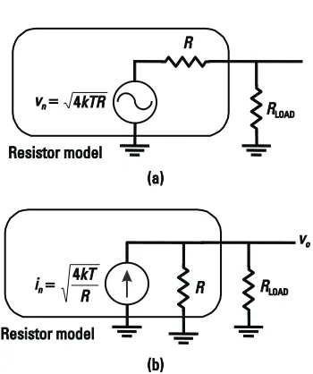
One of the most common noise sources in a circuit is a resistor. Noise in resistors is generated by thermal energy causing random electron motion [1–3]. The thermal noise spectral density in a resistor is given by
Nresistor= 4kTR (2.1)
where T is the Kelvin temperature of the resistor, k is Boltzmann’s constant (1.38 × 10⁻²³ J/K), and R is the value of the resistor. Noise power spectral density is expressed using volts squared per hertz (power spectral density). In order to find out how much power a resistor produces in a finite bandwidth, simply multiply (2.1) by the bandwidth of interest Df:
vn2 =4kTRDf (2.2)
wherevn is the rms value of the noise voltage in the bandwidthDf. This can also be written equivalently as a noise current rather than a noise voltage:
in2= 4kTDf
Thermal noise is white noise, meaning it has a constant power spectral density with respect to frequency (valid up to approximately 6,000 GHz) [4]. The model for noise in a resistor is shown in Figure 2.1.
2.2.2 Available Noise Power
Maximum power is transferred to the load whenRLOAD is equal to R. Then
vois equal to vn/2. The output power spectral density Po is then given by
Po= v
2
o
R =
vn2
4R =kT (2.4)
Thus, available power is kT, independent of resistor size. Note thatkTis in watts per hertz, which is a power density. To get total power out Pout in watts, multiply by the bandwidth, with the result that
Pout =kTB (2.5)
2.2.3 Available Power from Antenna
The noise from an antenna can be modeled as a resistor [5]. Thus, as in the previous section, the available power from an antenna is given by
Pavailable=kT =4 × 10⁻²¹ W/Hz (2.6)
atT =290K, or in dBm per hertz,
Pavailable= 10 log10
S
4 ×10 −211 × 10−3
D
= −174 dBm/Hz (2.7)Note that using 290K as the temperature of the resistor modeling the antenna is appropriate for cell phone applications where the antenna is pointed at the horizon. However, if the antenna were pointed at the sky, the equivalent noise temperature would be much lower, more typically 50K [6].
For any receiver required to receive a given signal bandwidth, the minimum detectable signal can now be determined. As can be seen from (2.5), the noise floor depends on the bandwidth. For example, with a bandwidth of 200 kHz, the noise floor is
Noise floor=kTB = 4× 10−21 ×200,000 = 8× 10⁻¹⁶ (2.8)
More commonly, the noise floor would be expressed in dBm, as in the following for the example shown above:
Noise floor= −174 dBm/Hz+ 10 log10(200,000) = −121 dBm (2.9)
Thus, we can now also formally define signal-to-noise ratio. If the signal has a power of S,then the SNR is
SNR = S
Noise floor (2.10)
level must be above the noise floor level by at least this amount. Consequently, the minimum detectable signal level in a 200-kHz bandwidth is more like−114 dBm (assuming no noise is added by the electronics).
2.2.4 The Concept of Noise Figure
Noise added by electronics will be directly added to the noise from the input. Thus, for reliable detection, the previously calculated minimum detectable signal level must be modified to include the noise from the active circuitry. Noise from the electronics is described by noise factorF,which is a measure of how much the signal-to-noise ratio is degraded through the system. We note that
So = G? Si (2.11)
whereSi is the input signal power,Sois the output signal power, andGis the power gain So/Si. We derive the following equation for noise factor:
F = SNRi
whereNo(total)is the total noise at the output. If No(source) is the noise at the
output originating at the source, andNo(added)is the noise at the output added by the electronic circuitry, then we can write:
No(total)= No(source) +No(added) (2.13)
Noise factor can be written in several useful alternative forms:
F= No(total)
This shows that the minimum possible noise factor, which occurs if the electronics adds no noise, is equal to 1. Noise figure NF is related to noise factor Fby
NF =10 log10 F (2.15)
Thus, while noise factor is at least 1, noise figure is at least 0 dB. In other words, an electronic system that adds no noise has a noise figure of 0 dB.
a filter with 3 dB of loss has a noise figure of 3 dB. This is explained by noting that output noise is approximately equal to input noise, but signal is attenuated by 3 dB. Thus, there has been a degradation of SNR by 3 dB.
2.2.5 The Noise Figure of an Amplifier Circuit
We can now make use of the definition of noise figure just developed and apply it to an amplifier circuit [8]. For the purposes of developing (2.14) into a more useful form, it is assumed that all practical amplifiers can be characterized by an input-referred noise model, such as the one shown in Figure 2.2, where the amplifier is characterized with current gainAi. (It will be shown in later chapters how to take a practical amplifier and make it fit this model.) In this model, all noise sources in the circuit are lumped into a series noise voltage sourcevnand a parallel current noise sourceinplaced in front of a noiseless transfer function. If the amplifier has finite input impedance, then the input current will be split by some ratioa between the amplifier and the source admittanceY
s:
SNRin= a2i2
in
a2ins2 (2.16)
Assuming that the input-referred noise sources are correlated, the output signal-to-noise ratio is
SNRout =
a2A2 i i
2 in
a2A2i
X
i2ns+
|
in +vnYs|
2C
(2.17)
Thus, the noise factor can now be written in terms of the preceding two equations:
F= i
This can also be interpreted as the ratio of the total output noise to the total output noise due to the source admittance.
In (2.17), it was assumed that the two input noise sources were correlated with each other. In general, they will not be correlated with each other, but rather the currentinwill be partially correlated withvnand partially uncorrelated. We can expand both current and voltage into these two explicit parts:
in= ic + iu (2.19)
vn= vc+ vu (2.20)
In addition, the correlated components will be related by the ratio
ic = Ycvc (2.21)
whereYc is the correlation admittance. The noise figure can now be written as
NF= 1 +i
2
u +
|
Yc + Ys|
2vc2+ vu2|
Ys|
2ins2 (2.22)
The noise currents and voltages can also be written in terms of equivalent resistance and admittance (these resistors would have the same noise behavior):
Thus, the noise figure is now written in terms of these parameters:
It can be seen from this equation that NF is dependent on the equivalent source impedance.
Equation (2.28) can be used not only to determine the noise figure, but also to determine the source loading conditions that will minimize the noise figure. Differentiating with respect to Gs and Bs and setting the derivative to zero yields the following two conditions for minimum noise (Gopt and Bopt)
after several pages of math:
Gopt=
√
Gu +RuS
2.2.6 The Noise Figure of Components in Series
For components in series, as shown in Figure 2.3, one can calculate the total output noise (No(total)) and output noise due to the source (No(source)) to determine the noise figure.
The output signal Sois given by
So =Si ? Gi ? G2? G3 (2.31)
The input noise is
Ni(source) =kT (2.32)
The total output noise is
No(total)= Ni(source)G1G2G3 + No1(added)G2G3
+No2(added)G3 +No3(added) (2.33)
The output noise due to the source is
No(source) =Ni(source)G1G2G3 (2.34)
Finally, the noise factor can be determined as
F= No(total) No(source) =1 +
No1(added) Ni(source)G1 +
No2(added) Ni(source)G1G2+
No3(added) Ni(source)G1G2G3
= F1+ F2G− 1 1 +
F3− 1
G1G2 (2.35)
The above formula shows how the presence of gain preceding a stage causes the effective noise figure to be reduced compared to the measured noise figure of a stage by itself. For this reason, we typically design systems with a low-noise amplifier at the front of the system. We note that the noise figure of each block is typically determined for the case in which a standard input source (e.g., 50V) is connected. The above formula can also be used to derive an equivalent model of each block as shown in Figure 2.4. If the input noise when measuring noise figure is
Ni(source) =kT (2.36)
and noting from manipulation of (2.14) that
No1(added)= (F− 1)No(source) (2.37)
Now dividing both sides of (2.37) by G1,
Ni(added)= (F− 1)
No(source)
G1 =(F−1)Ni(source) =(F−1)kT (2.38)
Then the total input-referred noise to the first stage is
Ni1= Ni(source) + (F1− 1)kT= kT+ (F1− 1)kT= kTF1 (2.39)
Thus, the input-referred noise model for cascaded stages as shown in Figure 2.4 can be derived.
Example 2.1 Noise Calculations
Figure 2.5 shows a 50-V source resistance loaded with 50V. Determine how much noise voltage per unit bandwidth is present at the output. Then, for any RL, what is the maximum noise power that this source can deliver to any load? Also find the noise factor, assuming thatRLdoes not contribute to noise factor, and compare to the case whereRLdoes contribute to noise factor.
Solution
The noise from the 50Vsource is
√
4kTR ≈ 0.9 nV/√
Hz at a temperature of 290K, which, after the voltage divider, becomes one half of this value, or vo= 0.45 nV/√
Hz .Now, for maximum power transfer, the load must remain matched, so RL=RS=50V. Then the complete available power from the source is delivered to the load. In this case,
Po = v
2
o
4RL =Pin(available)
Pin(available) =
vo2 4RL =
4kTRS
4RL =kT= 4 ×10
−21
At the output, the complete noise power (available) appears, and so ifRL is noiseless, the noise factor = 1. However, if RL has noise of
√
4kTRL V/√
Hz , then at the output, the total noise power is 2kT, wherekT is fromRSandkTis fromRL. Therefore, for a resistively matched circuit, the noise figure is 3 dB. Note that the output noise voltage is 0.45 nV/√
Hz from each resistor for a total of√
2 ? 0.45 nV/√
Hz = 0.636 nV/√
Hz (with noise the power adds because the noise voltage is uncorre-lated).Example 2.2 Noise Calculation with Gain Stages
In this example, Figure 2.6, a voltage gain of 20 has been added to the original circuit of Figure 2.5. All resistor values are still 50V. Determine the noise at the output of the circuit due to all resistors and then determine the circuit noise figure and signal-to-noise ratio assuming a 1-MHz bandwidth and the input is a 1-V sine wave.
Solution
In this example, atvxthe noise is still due to only RS andR2. As before, the
noise at this point is 0.636 nV/
√
Hz . The signal at this point is 0.5V, thus at pointvythe signal is 10V and the noise due to the two input resistorsRSand R2 is 0.636? 20 = 12.72 nV/√
Hz . At the output, the signal and noise from the input sources, as well as the noise from the two output resistors, all see a voltage divider. Thus, one can calculate the individual components. For the combination ofRSandR2, one obtainsvR
S+R2 = 0.5×12.72 =6.36 nV/
√
HzThe noise from the source can be determined from this equation:
vR
S =
6.36 nV/
√
Hz√
2 = 4.5 nV/√
Hz For the other resistors, the voltage isvR Total output noise is given by
vno(total)=
√
v(2RS+RL)+ vTherefore, the noise figure can now be determined:
Noise factor= F= No(total)
Since the output voltage also sees a voltage divider of 1/2, it has a value of 5V. Thus, the signal-to-noise ratio is
S
This example illustrates that noise from the source and amplifier input resistance are the dominant noise sources in the circuit. Each resistor at the input provides 4.5 nV/
√
Hz , while the two resistors behind the amplifier each only contribute 0.45 nV/√
Hz . Thus, as explained earlier, after a gain stage, noise is less important.Example 2.3 Effect of Impedance Mismatch on Noise Figure
Find the noise figure of Example 2.2 again, but now assume thatR2 =500V.
Solution
As before, the output noise due to the resistors is as follows:
vno(R
S)= 0.9? 500
where 500/550 accounts for the voltage division from the noise source to the node vx.
vno(R2)= 0.9?
√
10 ? 50550 ? 20? 0.5= 2.587 nV/
√
Hzwhere the
√
10 accounts for the higher noise in a 500-Vresistor compared to a 50-V resistor.vno(R3)= 0.9? 0.5=0.45 nV/
√
Hzvno(RL) =0.9? 0.5= 0.45 nV/
√
HzThe total output noise voltage is
vno(total)=
√
vR2Note: This circuit is unmatched at the input. This example illustrates that a mismatched circuit may have better noise performance than a matched one. However, this assumes that it is possible to build a voltage amplifier that requires little power at the input. This may be possible on an IC. However, if transmission lines are included, power transfer will suffer. A matching circuit may need to be added.
Example 2.4 Cascaded Noise Figure and Sensitivity Calculation
Find the effective noise figure and noise floor of the system shown in Figure 2.7. The system consists of a filter with 3-dB loss, followed by a switch with 1-dB loss, an LNA, and a mixer. Assume the system needs an SNR of 7 dB for a bit error rate of 10−3. Also assume that the system bandwidth is 200 kHz.
Solution
Figure 2.7 System for performance calculation.
Noise floor= −174 dBm + 10 log10(200,000)= −121 dBm
We make use of the cascaded noise figure equation and determine that the overall system noise figure is given by
NFTOTAL= 3 dB +1 dB +10 log10
F
1.78+ 15.84− 120
G
≈ 8 dBNote that the LNA noise figure of 2.5 dB corresponds to a noise factor of 1.78 and the gain of 13 dB corresponds to a power gain of 20. Furthermore, the noise figure of 12 dB corresponds to a noise factor of 15.84.
Note that if the mixer also has gain, then possibly the noise due to the IF stage may be ignored. In a real system this would have to be checked, but here we will ignore noise in the IF stage.
Since it was stated that the system requires an SNR of 7 dB, the sensitivity of the system can now be determined:
Sensitivity = −121 dBm + 7 dB+ 8 dB= −106 dBm
Thus, the smallest allowable input signal is −106 dBm. If this is not adequate for a given application, then a number of things can be done to improve this:
1. A smaller bandwidth could be used. This is usually fixed by IF require-ments.
2. The loss in the preselect filter or switch could be reduced. For example, the LNA could be placed in front of one or both of these components. 3. The noise figure of the LNA could be improved.
4. The LNA gain could be increased reducing the effect of the mixer on the system NF.
5. A lower NF in the mixer would also improve the system NF. 6. If a lower SNR for the required BER could be tolerated, then this
2.3 Linearity and Distortion in RF Circuits
In an ideal system, the output is linearly related to the input. However, in any real device the transfer function is usually a lot more complicated. This can be due to active or passive devices in the circuit or the signal swing being limited by the power supply rails. Unavoidably, the gain curve for any component is never a perfectly straight line, as illustrated in Figure 2.8.
The resulting waveforms can appear as shown in Figure 2.9. For amplifier saturation, typically the top and bottom portions of the waveform are clipped equally, as shown in Figure 2.9(b). However, if the circuit is not biased between the two clipping levels, then clipping can be nonsymmetrical as shown in Figure 2.9(c).
2.3.1 Power Series Expansion
Mathematically, any nonlinear transfer function can be written as a series expan-sion of power terms unless the system contains memory, in which case a Volterra series is required [9, 10]:
vout =k0+ k1vin+k2vin2 +k3vin3 + . . . (2.40)
To describe the nonlinearity perfectly, an infinite number of terms is required; however, in many practical circuits, the first three terms are sufficient to characterize the circuit with a fair degree of accuracy.
Figure 2.9 Distorted output waveforms: (a) input; (b) output, clipping; and (c) output, bias wrong.
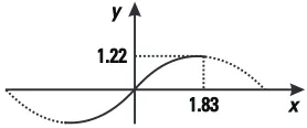
Symmetrical saturation as shown in Figure 2.8(b) can be modeled with odd order terms; for example,
y= x− 1 10x
3 (2.41)
looks like Figure 2.10. In another example, an exponential nonlinearity as shown in Figure 2.8(a) has the form
x+ x
2
2! + x3
3! + . . . (2.42)
which contains both even and odd power terms because it does not have symmetry about they-axis. Real circuits will have more complex power series expansions.
One common way of characterizing the linearity of a circuit is called the two-tone test. In this test, an input consisting of two sine waves is applied to the circuit.
vin=v1 cosv1t+ v2cos v2t=X1 + X2 (2.43)
When this tone is applied to the transfer function given in (2.40), the result is a number of terms:
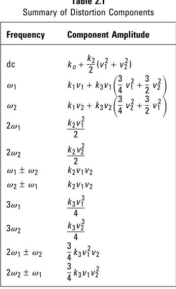
v0 =k0 + k1(X1 +X
5
2)+ k2(X1+ X5
2)2 + k3(X1 +X5
2)3 (2.44)desired second order third order
v0 =k0 + k1(X1 +X2)+ k2(X12 +2X1X2 +X22) (2.45) + k3(X13+ 3X12X2 +3X1X22 + X13)
These terms can be further broken down into various frequency compo-nents. For instance, the X12 term has a zero frequency (dc) component and another at the second harmonic of the input:
X12 = (v1 cosv1t)2 = v 2 1
2 (1 +cos 2v1t) (2.46)
The second-order terms can be expanded as follows:
(X1 +X2)2= X12
5
+ 2X1X5
2 + X225
(2.47)dc + MIX dc+
HD2 HD2
where second-order terms are composed of second harmonics HD2, and mixing components, here labeled MIX but sometimes labeled IM2 for second-order intermodulation. The mixing components will appear at the sum and difference frequencies of the two input signals. Note also that second-order terms cause an additional dc term to appear.
The third-order terms can be expanded as follows:
(X1+ X2)3 = X13
5
+ 3X12X5
2 +3X1X5
22 + X235
(2.48)FUND IM3 + IM3 + FUND
+HD3 FUND FUND + HD3
Table 2.1
Note that in the case of an amplifier, only the terms at the input frequency are desired. Of all the unwanted terms, the last two at frequencies 2v1 − v2 and 2v
2−v1are the most troublesome, since they can fall in the band of the
desired outputs ifv1is close in frequency tov2and therefore cannot be easily filtered out. These two tones are usually referred to as third-order intermodula-tion terms (IM3 products).
Example 2.5 Determination of Frequency Components Generated in a Nonlinear System
Consider a nonlinear circuit with 7- and 8-MHz tones applied at the input. Determine all output frequency components, assuming distortion components up to the third order.
Solution
Table 2.2 and Figure 2.11 show the outputs.
Table 2.2
Outputs from Nonlinear Circuits with Inputs atf1=7,f2=8 MHz
Symbolic Example
Frequency Frequency Name Comment
First order f1,f2 7, 8 Fundamental Desired output Second order 2f1, 2f2 14, 16 HD2 (harmonics) Can filter
f2−f1,f2+f1 2, 15 IM2 (mixing) Can filter Third order 3f1, 3f2 21, 24 HD3 (harmonic) Can filter
harmonics 2f1−f2, 6 IM3 (intermod) Close to
fundamental, 2f2−f1 9 IM3 (intermod) difficult to filter
Figure 2.11 Output spectrum with inputs at 7 and 8 MHz.
2.3.2 Third-Order Intercept Point
One of the most common ways to test the linearity of a circuit is to apply two signals at the input, having equal amplitude and offset by some frequency, and plot fundamental output and intermodulation output power as a function of input power as shown in Figure 2.12. From the plot, thethird-order intercept point(IP3) is determined. The third-order intercept point is a theoretical point where the amplitudes of the intermodulation tones at 2v1 − v2 and 2v2 − v
1 are equal to the amplitudes of the fundamental tones at v1 andv2.
From Table 2.1, if v1 = v2= vi, then the fundamental is given by
fund= k1vi + 94k3vi3 (2.49)
The linear component of (2.49) given by
fund = k1vi (2.50)
Figure 2.12 Plot of input output power of fundamental and IM3 versus input power.
IM3= 3 4k3v
3
i (2.51)
Note that for smallvi, the fundamental rises linearly (20 dB/decade) and that the IM3 terms rise as the cube of the input (60 dB/decade). A theoretical voltage at which these two tones will be equal can be defined:
3 4k3v
3 IP3
k1vIP3 = 1 (2.52)
This can be solved for vIP3:
vIP3 = 2
√
k13k3 (2.53)
Of course, the third-order intercept point cannot actually be measured directly, since by the time the amplifier reached this point, it would be heavily overloaded. Therefore, it is useful to describe a quick way to extrapolate it at a given power level. Assume that a device with power gainGhas been measured to have an output power ofP1 at the fundamental frequency and a power of P3at the IM3 frequency for a given input power ofPi, as illustrated in Figure 2.12. Now, on a log plot (for example, when power is in dBm) ofP3 andP1 versusPi, the IM3 terms have a slope of 3 and the fundamental terms have a slope of 1. Therefore,
OIP3− P1
IIP3 −Pi = 1 (2.54)
OIP3− P3
IIP3 −Pi = 3 (2.55)
since subtraction on a log scale amounts to division of power. Also note that
G= OIP3− IIP3= P1 −Pi (2.56)
These equations can be solved to give
IIP3 =P1 +12[P1 − P3]− G=Pi + 12[P1 −P3] (2.57)
2.3.3 Second-Order Intercept Point
Asecond-order intercept point (IP2) can be defined that is similar to the third-order intercept point. Which one is used depends largely on which is more important in the system of interest; for example, second-order distortion is particularly important in direct downconversion receivers.
If two tones are present at the input, then the second-order output is given by
vIM2=k2vi2 (2.58)
Note that in this case, the IM2 terms rise at 40 dB/decade rather than at 60 dB/decade, as in the case of the IM3 terms.
k2vIP22 k1vIP2
= 1 (2.59)
This can be solved forvIP2:
vIP2= k1
k2 (2.60)
2.3.4 The 1-dB Compression Point
In addition to measuring the IP3 or IP2 of a circuit, the 1-dB compression point is another common way to measure linearity. This point is more directly measurable than IP3 and requires only one tone rather than two (although any number of tones can be used). The 1-dB compression point is simply the power level, specified at either the input or the output, where the output power is 1 dB less than it would have been in an ideally linear device. It is also marked in Figure 2.12.
We first note that at 1-dB compression, the ratio of the actual output voltagevoto the ideal output voltagevoi is
20 log10
S
vo
voi
D
= −1 dB (2.61)or
vo
voi = 0.89125 (2.62)
Now referring again to Table 2.1, we note that the actual output voltage for a single tone is
vo =k1vi + 3 4k3v
3
i (2.63)
for an input voltagevi. The ideal output voltage is given by
voi = k1vi (2.64)
k1v1dB+ 3 4k3v
3 1dB
k1v1dB = 0.89125 (2.65)
Note that for a nonlinearity that causes compression, rather than one that causes expansion,k3 has to be negative. Solving (2.65) forv1dBgives
v1dB =0.38
√
k1k3 (2.66)
If more than one tone is applied, the 1-dB compression point will occur for a lower input voltage. In the case of two equal amplitude tones applied to the system, the actual output power for one frequency is
vo =k1vi + 9 4k3v
3
i (2.67)
The ideal output voltage is still given by (2.64). So now the ratio is
k1v1dB +
Therefore, the 1-dB compression voltage is now
v1dB =0.22
√
k1k3 (2.69)
Thus, as more tones are added, this voltage will continue to get lower.
2.3.5 Relationships Between 1-dB Compression and IP3 Points
Thus, these voltages are related by a factor of 3.04, or about 9.66 dB, independent of the particulars of the nonlinearity in question. In the case of the 1-dB compression point with two tones applied, the ratio is larger. In this case,
Thus, these voltages are related by a factor of 5.25 or about 14.4 dB. Thus, one can estimate that for a single tone, the compression point is about 10 dB below the intercept point, while for two tones, the 1-dB compression point is close to 15 dB below the intercept point. The difference between these two numbers is just the factor of three (4.77 dB) resulting from the second tone.
Note that this analysis is valid for third-order nonlinearity. For stronger nonlinearity (i.e., containing fifth-order terms), additional components are found at the fundamental as well as at the intermodulation frequencies. Nevertheless, the above is a good estimate of performance.
Example 2.6 Determining IIP3 and 1-dB Compression Point from Measurement Data
An amplifier designed to operate at 2 GHz with a gain of 10 dB has two signals of equal power applied at the input. One is at a frequency of 2.0 GHz and another at a frequency of 2.01 GHz. At the output, four tones are observed at 1.99, 2.0, 2.01, and 2.02 GHz. The power levels of the tones are −70, −20, −20, and −70 dBm, respectively. Determine the IIP3 and 1-dB compression point for this amplifier.
Solution
The tones at 1.99 and 2.02 GHz are the IP3 tones. We can use (2.57) directly to find the IIP3:
IIP3 = P1 + 12[P1− P3] −G= −20 +12[−20 + 70]−10 = −5 dBm
The 1-dB compression point for a signal tone is 9.66 dB lower than this value, about−14.7 dBm at the input.
2.3.6 Broadband Measures of Linearity
could be defined. Two other measures of linearity that are common in wide-band systems handling many signals simultaneously are calledcomposite triple-order beat(CTB) andcomposite second-order beat(CSO) [11, 12]. In these tests of linearity,N signals of voltageviare applied to the circuit equally spaced in frequency, as shown in Figure 2.13. Note here that, as an example, the tones are spaced 6 MHz apart (this is the spacing for a cable television system for which this is a popular way to characterize linearity). Note also that the tones are never placed at a frequency that is an exact multiple of the spacing (in this case, 6 MHz). This is done so that third-order terms and second-order terms fall at different frequencies. This will be clarified shortly.
If we take three of these signals, then the third-order nonlinearity gets a little more complicated than before:
(x1+ x2 + x3)3= x31+ x32+
5
x33HD3
+3x21x2 +3x21x3 +3x22x1 +3x23x1+ 3x22x
5
3+ 3x23x2IM3
+6x1x2x
5
3 (2.72)TB
The last term in the expression causes CTB in that it creates terms at frequenciesv
1± v2± v3 of magnitude 1.5k3vi wherev1 <v2< v3. This
is twice as large as the IM3 products. Note that, except for the case where all three are added (v
1+v2+v3), these tones can fall into any of the channels
being used and many will fall into the same channel. For instance, in Figure