Design Investigation of Microstrip Antenna using
Loading Circuit (LC) Method for Amateur Satellite
Communication UHF Band
Akuwan Saleh
*)*) Department of Electrical Engineering,
Electronic Engineering Polytechnic Institute of Surabaya, Surabaya, Indonesia
Budi Aswoyo
*)*) Department of Electrical Engineering,
Electronic Engineering Polytechnic Institute of Surabaya, Surabaya, Indonesia
Abstract—This paper presents a design investigation of micro-strip antennas by using inserting a resistive load (loading circuit method) that it is called as loading circuit (LC) microstrip antenna. The aim of inserting of a resistive load is to reduce dimensions of conventional one that is relatively large in size for UHF bands. The antenna material uses PCB FR-4 Epoxy, in which there is a dielectric substrate with dielectric constant (εr = 4.7, tan δ = 0.02), height h = 1.6 mm. As a comparator, first a conventional square microstrip antenna is designed with a certain dimension. To generate a resonant frequency, the feed point of the antenna is placed at the vertices of the diagonal line at a certain position. Next, the microstrip antennas is designed by using the same material at the same operating frequency as conventional one and adding resistive loads. At this stage, an effect of the position of the feeding point and value of the loads to the antenna characteristics is investigated. In addition, value of the loads are varied from: shorting circuit (pin), low resistive resistor 1.0 Ω, 1.1 Ω, 1.2 Ω, and also the impact of slit to produce a size reduction with the expected specifications. The design specifications of both microstrip antennas (a conventional and loading circuit) are operating frequency of 435 MHz to 438 MHz according to amateur radio frequency band for satellite, with design frequency of 435.9 MHz, bandwidth of 3 MHz, with 50 Ω input impedance, VSWR is smaller than 2.0, and band-width more than 3 MHz. Circularly polarized antenna with axial ratio is less than 3 dB, and the radiation pattern produced is direction. All the design process of this antenna using CST Microwave Studio.
Keywords—microstrip antenna; loading circuit; chip resistor; circular polarization
I. INTRODUCTION
Recently, Amateur Satellite Communication UHF Band, otherwise known as Nano Satellite technology is developed and studied in many countries. Nano satellites are artificial communications satellites that have relatively small sizes. In the implementation of this satellite, the antenna is one of the key components, whose dimensions should be small and low profile. The microstrip antenna designed to operate on the frequency of UHF (Ultra High Frequency) nano satellites, precisely at 435.9 MHz frequencies, generally has a relatively large size because the length of the antenna should be about
half the wavelength on the low permittivity substrate medium [1]. Therefore, special efforts are needed to reduce the size of the antenna.
Microstrip antenna is one type of antenna that is in great demand as a component of the Nano Satellite. In light saline, this antenna has a small and simple ralative shape, and is easily produced [2]. Microstrip antennas can be designed in such a way with many geometric shapes and dimensions adjusted for flexibility for the layout of communication devices. There are several methods that can be used to reduce the size of microstrip antennas which are generally relatively large when they are odorized to UHF bands, one of which is the short circuit method. Short circuit microstrip is widely used because it can realize resonant frequencies smaller than half the size of a conventional microstrip antenna [3].
Theoretically, microstrip antennas with short-circuit loads can be constructed by short-circuit zero potential fields of ordinary microstrip antennas excavated with dominant modes. By wrapping the copper strips around the edges of the antenna it can be able to simulate the result by using the shoftware design of a certain antenna. From a manufacturing point of view, shorting posts construction is much easier than wrapping a copper strip around the edge of the antenna [4]. The problem that arises is that this technique produces antenna with relatively narrow bandwidth [1]. Therefore, it is necessary to place a resistor at a certain position to produce a wider bandwidth [10-11].
In this paper, the microstrip antennas with shorting or loading circuits design is presented. In the shorting circuit microstrip antenna design, there are two shorting pins that connect the patch and the ground is investigated, one pin and two pins. The position and effect of shorting pins is investigated corespond to the resulting parameter of antenna. In the loading circuit microstrip antenna, the low resistive resistor 1.0 Ω , 1.1 Ω , 1.2 Ω , and the impact of feeding technique of coaxial probe is combined with the addition of slit on the patch antenna corespond to the resulting of return loss parameter is also investigated.
The goal of this study after inserting LC mothod in microstrip antenna, to obtain the best design specification,
which in the next research will be made prototype antenna. Furthermore, the prototype antenna will be tested for specifications in the laboratory and its feasibility is concluded to be applied in the field.
II. PREVIOUS WORK
Previously, there have been several studies that have been done to reduce the size of microstrip antenna. Waterhouses [6] and Porath [7] use methods that have been shown in different forms of patches, and also investigate the use of short circuit. Furthermore, Waterhouse continued his research on circuitry short circuit methods and stated that the size of the maximum reducing microstrip antenna can be reduced by using a single shorting pin. By adding a chip resistor to a certain position in place of the shorting pin, a wider antenna bandwidth is generated [1].
III. ANTENA DESIGN INVESTIGATION
In this paper, there are two microstrip antenna design stages, the first is a conventional microstrip antenna and the second is a shorting and loading circuit microstrip antenna. A conventional microstrip antenna is designed as a comparative one of size reduction produced by shorting and loading circuit method.
A. Conventional microstrip antenna
The first stage is designing a conventional square microstrip antenna that works at frequency of 435.9MHz with coaxial probe feeding technique. The preliminary design of antenna is shown in Fig.1. Dimension of patch and substrat are Wp x Lp and Wg x Lg, respectively. The coordinate position of antenna at P(x,y). The substrate is FR-4 with dielectric constant (εr = 4.7, tan δ = 0.02) and 1.6 mm thick
substrate. Material from the patch and ground using copper. Ground is located at the bottom of the dielectric substrate, while the patch is located at the top of the substrate.
Fig.1. Preliminary design of a conventional microstrip antenna
The following is calculation of a conventional microstrip antenna size [9]
(
) (
)
+ − ε + + ε = ε w h 12 1 1 2 1 2 1 r r reff(
) (
)
+ − + + = 38 . 20 16 . 0 12 1 1 2 1 7 . 4 2 1 7 . 4 = 4.168.(
)
(
)
+ − + + = 8 . 0 258 . 0 264 . 0 3 . 0 412 . 0 h w h w h Lp reff reff ε ε Δ(
)
(
)
+ − + + × = 8 . 0 16 . 0 0 258 . 0 618 . 4 264 . 0 16 . 0 0 3 . 0 618 . 4 16 . 0 412 . 0 = 7.6 mm. eff 2f0 reff c Lp ε = mm 13 . 160 618 . 4 10 9 . 435 2 10 . 3 6 8 = × × = Lp=Lpeff−2ΔLp = 160.13 – 2 x 7.6 = 152.52 mm Lp = Wp =152.52 mm.Based on the calculation results above, the length and width of patch antenna is 152.52mm x 152.52mm. While the coaxial probe is placed on diagonal line of patch antenna at x and y axis position (20mm, 0).
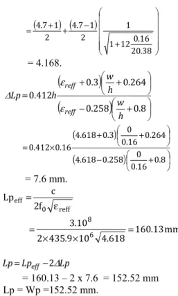
TABLE 1 presents the summary result of a convensional microstrip antenna design and Fig.1 shows the complete of the dimension/position design of antenna elements. The length and width of patch antenna is 152.52mm x 152.52mm. The length of substrat is 220mm x 220mm. The coaxial probe is placed on a diagonal line of patch antenna at x and y axis position (20mm, 0).
TABLEI.SUMMARY OF DIMENSION/POSITION OF A CONVENTIONAL
MICROSTRIP ANTENNA DESIGN
No: Dimension/Position: Units/Coordinate:
1. Patch length (Lp) 152.52 mm
2. Patch width (Wp) 15252 mm
3. Substrat length (Lg) 220 mm
4. Substratwidth(Lg) 220 mm
5. Coaxial probe position (x,y) (20mm,0)
The result of design and dimensions of a conventional microstrip antenna simulated with CST Microwave Studio is shown in Fig.2(a) and (b). The S11 parameter and VSWR are shown in Fig.3 and Fig.4, respectively.
(a)
(b)
Fig.2. Result design of a conventional microstrip antenna (a) front view: (b) rear view
Fig.3. S11 parameters of a conventional microstrip antenna
Fig. 4. VSWR of a conventional microstrip antenna
The return loss at center frequency of 435.9 MHz is -21.486 dB. The simulated -10 dB return loss bandwidth is 4.02 MHz and VSWR value is equal to 1.2.
B. Shorting Circuit (Pin) Microstrip Antenna
A shorting circuit or pin microstrip antenna is also designed to work at frequency of 435.9MHz and has smaller size than conventional one. The substrate used is also FR-4
with dielectric constant (εr = 4.7, tan δ = 0.02) and 1.6 mm
thick substrate. Shorting pin is made by adding copper with 1.0 mm diameter. This copper is connected from patch antenna to ground.
There are two shorting pins that connect the patch and the ground is investigated, one pin and two pins. The position and effect of shorting pin is investigated corespond to the resulting of input impedance of S11 parameter. So the difficulty of this design is the placement of the shorting pins at the corresponding position.
Fig.5 shows the one shorting pin microstrip antenna design, dan TABLE II presents the summary result of design of dimension/position. The length and width of patch antenna are 88.5mm x 88.5mm. The length of substrat is 120mm x 120mm. The pin (x,y) is placed on the x and y coordinatees (55mm, 0). While the coaxial probe placed at position (20mm, 0).
TABLEII.SUMMARY OF DIMENSION/POSITION OF A SHORTING CIRCUIT
MICROSTRIP ANTENNA DESIGN WITH ONE SHORTING PIN
No: Dimension/Position: Unit/Coordinate:
1. Patch length (Lp) 88.5 mm
2. Patch width (Wp) 88.5 mm
3. Substrat length (Lg) 120 mm
4. Substratwidth(Lg) 120 mm
5. Coaxial probe (x,y) (20 mm,0)
6. Shorting pin (x,y) (55 mm,0)
(a)
(b)
Fig.5. One shorting pin microstrip antenna (a) Top view (b) Side view
Fig.6 shows the S11 parameter simulation result. It can be seen that the return loss of the microstrip antenna when one shorting pin is used does not resonant at the desired frequency specification. Therefore it is required the trial process required the number of shorting pins.
S11 (
dB
)
VS
Fig.6. S11 parameter of one shorting pin microstrip antenna
Furthermore, by using two shorting pins that are placed on the x and y coordinatees (5mm, 0) and (35mm, 0) is achieved better input impedance. While the coaxial probe is placed at fixed position (20mm, 0).
Based on the last design and simulation process, the length and width of patch antenna is 88.5mm x 88.5mm. The length of substrat is 120mm x 120mm.The two shorting pins are placed on the x and y coordinatees (5mm, 0) and (35mm, 0). While the coaxial probe placed at position (20mm, 0). Fig.7 shows the two shorting pins microstrip antenna simulation design result dan Fig.8 is the S11 parameters simulation result.
(a)
(b)
Fig.7. Two shorting pins microstrip antenna (a) Top view (b) Side view
Fig.8. S11 parameter of two shorting pins microstrip antenna
The S11 or return loss of simulation result at frequency 435.9 MHz is -18.296, but the bandwidth is narrow (1.19 MHz). Therefore, the optimization process is required in order to enlarge the bandwidth.
IV. ALOADING CIRCUIT (LC)MICROSTRIP ANTENNA DESIGN
INVESTIGATION AND ANALYSIS
A. Design of Antenna
By replacing the shorting pin with a low resistance chip resistor, the required antenna size can be significantly reduced for operating at fixed frequency, moreover the antenna bandwidth can be greatly enhanced [5]. Priliminary design of a loading circuit (LC) microstrip antenna is shown in Fig.9.
Fig.9. Primilnary design of a loading circuit (LC) microstrip antenna
Where Lp is length of pacth, Wp is wide of pacth, Lg is length of subtrat, Wg is wide of subtrat, P is feeder point of coaxial probe, r is distance between edge of patch and chip resistor, y is slit length, and d is wide of slit.
The material antenna used is also FR-4 (lossy) with FR-4 with dielectric constant (εr = 4.7, tan δ = 0.02) and 1.6 mm
thick substrate.
Based on design results, the LC microstip antenna is much smaller than with the addition of shorting pins. This dimension is derived from the iteration of several parameters, such as by changing the position of the coaxial probe, the resistor chip and the length of the four slits until the matching impedance matches is obtained.
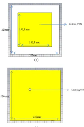
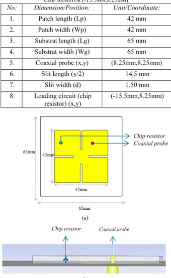
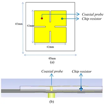
TABLE III presents the summary of dimensions of a LC microstrip antenna design result and Fig.10 shows the complete of the dimension and position of feeding and loading of antenna. The size of the substrat length that is as antenna ground plane Lg = Wg = 65 mm. The antenna patch dimension at simulation is Lp = Wp = 42 mm. The coaxial probe is placed on a diagonal line of patch antenna at x and y axis position (8.25mm, 8.25mm).
The process of inserting the coaxial probe is the same as a conventional microstrip antenna coaxial probe manufacturing process, there is only the difference of location and iteration of its position against the resistor chip.
S11 ( dB ) S11 ( dB )
TABLEIII.SUMMARY OF DIMENSION/POSITION OF ALCMICROSTRIP
ANTENNA DESIGN, WHERE COAXIAL PROBE (8.25MM,8.25MM) AND
CHIP RESISTOR (-15.5MM,8.25MM)
No: Dimension/Position: Unit/Coordinate:
1. Patch length (Lp) 42 mm
2. Patch width (Wp) 42 mm
3. Substrat length (Lg) 65 mm
4. Substrat width (Wg) 65 mm
5. Coaxial probe (x,y) (8.25mm,8.25mm)
6. Slit length (y/2) 14.5 mm
7. Slit width (d) 1.50 mm
8. Loading circuit (chip
resistor) (x,y) (-15.5mm,8.25mm)
(a)
(b)
Fig.10. Design result of a LC microstrip antenna with four slits with coaxial probe at (8.25mm,8.25mm) and chip resistor at (-15.5mm,8.25mm) (a) Top view (b) Side view
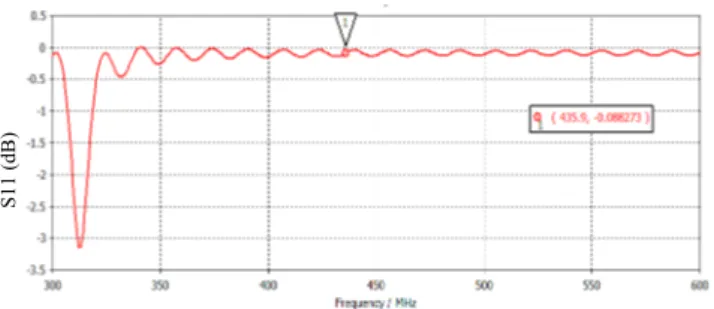
After obtaining the appropriate design, then performed the simulation process with transient solver at 300 MHz to 600 MHz observation frequency range. Fig.11 shows the S11 parameter of the results of the simulation of a LC microstrip antenna with the addition of 1.0 Ω chip resistor. Based on the simulation results, obtained return loss value at 435.9MHz operating frequency of -17.834 dB or VSWR of 1.29. This value meets the antenna design specification because the return loss is less than -10 dB or VSWR less than 2.0.
Fig.11. S11 parameter of a LC microstrip antenna with four slits with coaxial probe at (8.25mm,8.25mm) with chip resistor of 1.0 Ω at (-15.5mm,8.25mm)
Based on graph S11 in Fig.11, the bandwidth antenna can be calculated by the difference between highest and lowest frequency at the time of retun loss is -10 dB. The highest frequency simulation result is 455.49 MHz and its lowest frequency is 413.57 MHz. From this result obtained bandwidth of 41.92 MHz, much larger than when used shorting pin; 1.19 MHz.
Based on the simulation results, the value of the axial ratio is 1.4 or 2.9 dB below as 3 dB. Therefore, circular polarization is achieved.
B. Effect of Replacement Value of Chip Resistor
On observation of the replecement of 1.0 Ω resistor with 1.1 Ω and 1.2 Ω obtained the following phenomenon. Fig. 12 shows the S11 parameter of the simulation result of a LC microstrip antenna with the dimension/position at TABLE III and with 1.1 Ωchip resistor instead of 1.0 Ω. Based on the simulation results, obtained return loss value at 435.9MHz operating frequency of -22.776 dB or VSWR of 1.16. The bandwidth of antenna is 46.70 MHz.
Fig.12. S11 parameter of a LC microstrip antenna with four slits with coaxial probe at (8.25mm,8.25mm) with chip resistor of 1.1 Ω at (-15.5mm,8.25mm)
Furthermore, Fig. 13 shows the S11 parameter of the results of the simulation of LC microstrip antenna with the addition of 1.2 Ω chip resistor instead of 1.1 Ω. Based on the simulation results, obtained return loss of -29.537 dB or VSWR of 1.10 at operating frequency of 435.9 MHz.
Fig.13. S11 parameter of a LC microstrip antenna with four slits with coaxial probe at (8.25mm,8.25mm) with chip resistor of 1.2 Ω at (-15.5mm,8.25mm)
Based on simulation results above, the parameter design of a LC microstrip antenna with the dimension/posision at TABLE III and with the loading of 1.0 Ω, 1.1 Ω, and 1.2 Ω chip resistor, can be summarised in TABLE IV.
Coaxial probe Chip resistor Coaxial probe Chip resistor S11 ( dB ) S11 ( dB ) S11 ( dB )
TABLEIV. SUMMARY OF SIMULATION DESIGN OF LCMICROSTRIP
ANTENA WITH VARIED CHIP RESISTOR Parameter
Design 1.0 Ω 1.1 Chip Resistor Ω 1.2 Ω
Design frequency 435.9 MHz 435.9 MHz 435.9 MHz Return Loss -17.83 dB -22.78 dB -29.54 dB VSWR 1.29 1.16 1.1 Range Op. Freq. 413.57 MHz 445.49 – 457.83 MHz 411.13 – 458.4 MHz 408.59 – Bandwidth 41.92 MHz. 46.70 MHz 49.81 MHz Axial ratio 2.9 dB 3.42 3.92
Polarization RHCP Linear Linear C. Effect of Exchanging the Position of Probe Coaxial and
Feeding
Based on antena design listed in TABLE IV, by exchanging the location of "coaxial probe (x,y)" from (8.25mm, 8.25mm) to (-8.25mm, 8.25mm), and "loading circuit (chip resistor) (x,y)" from (-15.5mm, 8.25mm) to (15.5mm, 8.25mm), while the size of the substrat length that is same as Lg = Wg = 65 mm, the patch dimension at Lp = Wp = 42 mm, the length of each slit is 14.5mm, and the width of each slit (d) is 1.5mm, so the design result of a LC microstrip antenna is shown in Fig.14.
Fig .14. Design result of of LC microstrip antenna with four slits with coaxial probe at (-8.25mm,8.25mm) and chip resistor at (15.5mm,8.25mm) (a) Top view (b) Side view
Based on antenna design, the position of the coaxial probe equal to the plane (x.y) is (-8.25mm, 8.25mm) instead of (8.25mm, 8.25mm) that is in the diagonal line of the patch and the resistor chip of 1.0 Ω is placed at coordinates (15.5mm, 8.25mm) instead of (-15.5mm, 8.25mm) or 5.5mm away from the right edge of the patch, then is combined with four slits of length and will produce a circular current distribution or polarization to the left side (LHCP) instead of polarization to the right side (RHCP). Replacement of chip resistor from 1 Ω
to 1.1 Ω or 1.2 Ω causes circular polarization change to be linear polarization.
V. CONCLUSION
Design of microstrip antennas by using inserting a resistive load (loading circuit method) for amateur satellite communi-cation UHF band has been investigeted using CST Microwave Studio. The antenna material uses PCB FR-4 Epoxy, in which there is a dielectric substrate with dielectric constant (εr = 4.7, tan δ = 0.02), height h = 1.6 mm. By adding two shorting pins placed in a certain position, it will result in a reduction of 335% compared to conventional microstrip antennas, but resulting in relatively small bandwidth. By replacing the shorting pins with loading circuit then is combined with four slits of length and will produce a circular current distribution or polarization polarization to the right side (RHCP). Replacement of chip resistor from 1.0 Ω to 1.1 Ω or 1.2 Ω causes circular polarization change to be linear polarization. Effect of exchanging the position of probe coaxial and feeding produces LHCP instead of RHCP.
References
[1] Sheta, Abdel Fatah, “Investigation of New Small Size MicrostripAntena with Inductive Loading,” EE. Department King Saudi Univ, Saudi Arabia, 2002.
[2] G.R, Bharthia, P, Bahl, I. Dan Ittipiboon, A Microstrip Design Handbook, Artech House Inc, Noerdwood, MA, 2001.
[3] Kin Wu Long, Broadband Microstrip Antenas, New York. John Wiley & Sons, Inc.2002.
[4] Kumar, Pradeep, G.Singh, “MicrostripAntena Loaded with Shorting Circuit”. Jaypee University of Information Technology, Solan, India, 2009.
[5] Kin Wu Long, Broadband MicrostripAntenas, New York. John Wiley & Sons, Inc., 2002.
[6] R.Waterhouse, “Small microstrip patch antenna,” Electronics Letters, Vol. 31, pp. 604-605, 1995.
[7] R. Porath, “Theory of miniaturized shorting-post microstrip antennas,” IEEE Transactions, Antennas and Propagation,” Vol. 48, No. 1, pp. 41-47, 2000.
[8] R. Waterhouse, “Small microstrip patch antenna,” Electronics Letters, Vol. 31, pp. 604-605, 1995.
[9] Balanis, Constantine A, Antena Theory Analysis and Design, Second Edition, New York : Harper &Row Publisher Inc, 1997.
[10] GARAG, R.BHARTIA, P.BAHL,I., ITTIPIBOON, A.Microstrip antenna design handbook, (Artech House London 2001), pp. 591-657
[11]LIANG, M.C., KUO, Y.L., YEN, Y.M, and LAI, W.C.:”A capacitor-loaded frequency control scheme for circular patch antenna”, Electron. Lett., 2000, 36, pp. 1757-1758. Chip resistor Coaxial probe (a) Chip resistor Coaxial probe (b)