T
he quickening pace of MOSFET technology scaling, as seen in the new 2001International Technology Roadmap for Semiconductors[1], is ac-celerating the introduction of many new technologies to extend CMOS into nanoscale MOSFET structures heretofore not thought possible. A cautious optimism is emerging that these new technologies may extend MOSFETs to the 22-nm node (9-nm physical gate length) by 2016 if not by the end of this decade. These new devices likely will feature several new materials cleverly incorporated into new nonbulk MOSFET structures. They will be ultra fast and dense with a voracious appetite for power. Intrinsic device speeds may be more than 1 THz and integration densities will exceed 1 billion transistors per cm2. Excessive power consumption, however, will demand judicious use of these high-performance devices only in those critical paths requiring their su-perior performance. Two or perhaps three other lower performance, more power-efficient MOSFETs will likely be used to perform less performance-criti-cal functions on the chip to manage the total power consumption.Beyond CMOS, several completely new approaches to information-process-ing and data-storage technologies and architectures are emerginformation-process-ing to address the timeframe beyond the current roadmap. Rather than vying to “replace” CMOS, one or more of these embryonic paradigms, when combined with a CMOS plat-form, could extend microelectronics to new applications domains currently not accessible to CMOS.A successful new information-processing paradigm most likely will require a new platform technology embodying a fabric of intercon-nected primitive logic cells, perhaps in three dimensions. Further, this new logic paradigm may suggest a new symbiotic information-processing architec-ture to fully extract the potential offered by the logic fabric. An excellent sum-mary of nanoelectronic devices is contained in the Technology Roadmap for Nanoelectronics, produced by the European Commission’s Information Society Technology Programme (Future and Emerging Technologies)[2].
The goal of this article is to introduce and review many new device technolo-gies and concepts for information and signal processing having potential to ex-tend microelectronics to and beyond the time frame of the new 2001 ITRS. The scope of this article is to “cast a broad net” to gather in one place substantive, al-ternative concepts for memory, logic, and information-processing architectures that would, if successful, substantially extend the time frame of the ITRS beyond CMOS. As such, this section will provide a window into candidate approaches. Provision of in-depth, critical analysis of each approach will be quite important but is beyond the scope of this article.
By James A. Hutchby,
George I. Bourianoff,
Victor V. Zhirnov,
and Joe E. Brewer
Emerging Technology Parametrization
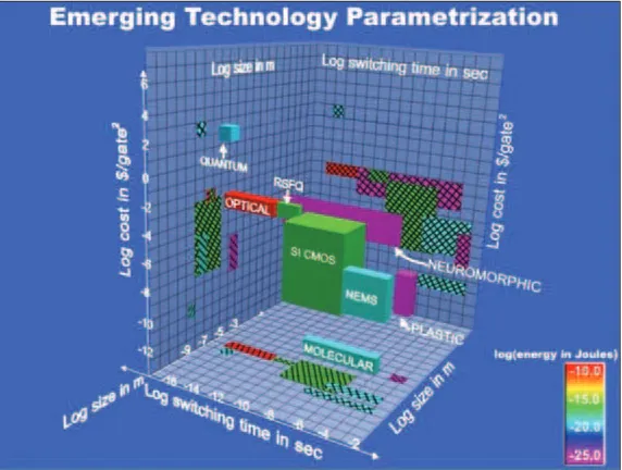
Figure 1 shows a parametrization of CMOS and a selected set of emerging technologies in terms of speed, size, cost, and power [3]. These emerging technologies in general are not a direct replace-ment for silicon and may require radically new ar-chitectures to achieve their functionality. The first three parameters in this figure (speed, size, and cost) are used to define a three-dimensional space and the fourth parameter (switching energy) is displayed as color code. This color code is shown in the legend found in the lower right hand corner of the graph. All the scales are logarithmic and span many orders of magnitude as shown in the graph. Each of the technologies displaces a certain vol-ume in this parameter space and is color-coded in a solid color representing the energy required for a single gate operation. Each of the volumes is pro-jected onto the bounding planes so that quantita-tive values of the parameters can be determined.The projections of the volume corresponding to a given technol-ogy are shown as crosshatched rectangles filled with the same color as the corresponding volume.
In the absence of firm measured data, a number of assump-tions were made to estimate the parameters for the emerging technologies. The parameters used for each technology are listed in Table 1. If an emerging technology is in the concept stage with no measured data, the parametric assumptions are based on the underlying physical principles. If some measured data exists, the assumptions involve an estimate on how far the technology can be scaled. In this case, the scaling arguments are based on physical principles.
Several of the technologies listed are strongly tied to a single application area or niche where the technology is particularly ef-fective. For example, quantum computing can find prime factors very efficiently by means of Shore’s algorithm [4], but it is much less efficient for other applications. In this case, we define an “ef-fective” time per operation as the time required by a classical de-vice in a classical architecture using a classical algorithm to do the calculation. Therefore, the “effective” operation time of an N-qubit quantum computer factoring a large number is very much faster than the operation time of an N-gate classical com-puter because of the inherent parallelism associated with quan-tum computing. A similar approach is used for neuromorphic and optical computing.
Figure 1, therefore, conveys meaningful information about the relative positions of the emerging technologies in this appli-cation space. It shows that few of the new technologies are di-rectly competitive with scaled CMOS and most are highly complementary. It also shows very clearly the benefit to be de-rived from heterogeneous integration of the emerging technolo-gies with silicon CMOS platform technology to expand its overall application space.
In this table,Trefers to a single delay, CD refers to critical di-mension, Energy is the intrinsic operational energy, and cost is
1. Parametrization of emerging technologies and CMOS: speed, size, cost, power.
Acronyms
ASIC Application specific integral circuit CNN Cellular nonlinear network CMOS Complimentary
metal-oxide-semiconductor [technology]
DRAM Dynamic RAM
GMR Giant magnetoresistance
ITRS International Technology Roadmap for Semiconductors
MEMS Micro-electromechanical system
MOSFET Metal-insulator-semiconductor field-effect transistor
MRAM Magnetic RAM
MTJ Magnetic tunnel junction NEMS Nano-electromechanical system NMR Nuclear magnetic resonance OUM Ovonic unified memory PSV Pseudo spin valve
QCA Quantum cellular automata RAM Random access memory R&D Research and development RSFQ Rapid single flux quantum (logic) RTD Resonant tunneling diode
TCAD Technology computer-aided design TFT Thin film transistor
TMR Tunneling magnetoresistance TPL Tunneling phase logic
SIA Semiconductor Industry Association SRAM Static RAM
defined as $ per gate. TheTminfor Si CMOS is determined by the local clock frequency specified in the 2001 ITRS for the 22-nm node, and not by the intrinsic transistor speed (CV/I).
Four of the information-processing technologies shown in Fig. 1 and Table 1 are included in tables given below. These in-clude silicon CMOS, RSFQ, molecular, and quantum comput-ing. The remaining four paradigms shown in Fig. 1 are plastic transistors, optical computing, NEMS, and neuromorphic com-puting; these are briefly described in this section.
Plastic transistors are defined to be thin-film transistor (TFT) devices fabricated on plastic substrates. The active layer of the TFT can be amorphous or poly-Si as well as organic semiconductors. Often, the TFTs are combined with organic light emitting diodes to form intelligent, flexible display devices than can be bent, folded, worn, or conformally mapped on to arbitrarily shaped sur-faces. A process technology consisting just of printing operations on paper-based substrates would have an intrinsic cost structure similar to color inkjet printing today. It could support disposable devices such as periodicals and dynamic bar codes.
Optical computing is based on using light transmission and interaction with solids for information processing. The potential advantages of digital optical computers relate to the following properties of light as a carrier of information. First, optical beams do not interact with each other, and, second, optical informa-tion-processing functions can be performed in parallel (perform-ing a Fourier transform, for example). Lastly, optical signals can be propagated at high speeds (speed of light in a media).
Nanoelectromechanical systems (NEMS) applied to logic gates for a computer in the form of mechanical digital signals are represented by displacements of solid rods, and the speed of sig-nal propagation is limited to the speed of the sound (e.g., 1.7× 10⁴m/s in diamond). Optimistic estimates predict NEMS logic gates that switch in 0.1 ns and dissipate less than 10-21J and
computers that perform 1016instructions per Watt (compared to 5×10¹²instruction per Watt in human brain operation). More conservative estimates of characteristics of the NEMS comput-ers can be made based on recent demonstrations of VLSI-NEMS chip for parallel data storage (e.g., IBM’s Millipede concept [6]). Reported storage densities are 500 Gb/in2. The highest data rates achieved so far are 6 Mb/s. A summary of conservative estimates of parameters of the NEMS computers is given in Table 1.
The human brain is defined to be the archetypal neuromorphic information processing device and is included here to provide a ba-sis of comparison with technological information-processing sys-tems. The scale length of individual neurons is estimated from the volume of the brain and the estimated number of neurons. Simi-larly, the speed quoted in Table 1 forTmaxis the experimentally ob-served time scale for opening and closing of synapses. The minimum switching speed is derived from an “effective operation time” of neuromorphic computing. In that case, the reference op-eration is vision processing where there is a great deal of informa-tion relating to manmade systems. The effective times defined in this way are very much faster than the synaptic speed and reflects that the interconnect density of the human brain is very much greater than any manmade system. Estimates of the data rate for the neuromorphic device on this basis is 1013bits/s, giving aTminof 10−13s. Each neuron is connected to 100 to 10,000 synapses, which differentiates the architecture of the human brain from that of sili-con-based systems.
Platform Technologies
Many new systems applications enabled by one or more of the emerging technologies discussed in this article likely will re-quire huge amounts of inexpensive information-processing and data-storage to perform their overall system functions. The CMOS and memory technologies available at that time will fill these so-called “platform” systems functions or technologies.
Table 1. Estimated Parameters for Emerging Research Devices and Technologies
Si CMOS 3E-11 1E-6 8E-9 5E-6 4E-18 4E-9 3E-3
RSFQ 1E-12 5E-11 3E-7 1E-6 2E-18 1E-3 1E-2
Molecular 1E-8 1E-3 1E-9 5E-9 1E-20 1E-11 1E-10
Plastic 1E-4 1E-3 1E-4 1E-3 1E-24 1E-9 1E-6
Optical (digital) 1E-16 1E-12 2E-7 2E-6 1E-12 1E-3 1E-2
NEMS 1E-7 1E-3 1E-8 1E-7 1E-21 1E-8 [5] 1E-5
Neuromorphic 1E-13 1E-4 6E-6 6E-6 3E-25 5E-4 1E-2
Quantum
The CMOS and memory structures and technologies discussed below are candidates for both extending microelectronics to the next decade and for fulfilling the platform function.
Nonclassical CMOS Devices
Extension of scaled CMOS to the to the end of the time hori-zon of the 2001 ITRS in the next decade will exacerbate several well-known emerging challenges to MOSFET technology. For digital applications, conventional rules for scaling MOSFETs in lateral size and integration density [7] also require scaling the vertical dimensions of elements of the transistor as well. Vertical scaling of these elements, including the gate dielec-tric thickness and the source and drain junction depths, causes an exponential increase in the transistor leakage cur-rents (gate, channel, and source/drain junctions). Further, scaling below the 100-nm node will require extraordinary measures to control a threshold voltage increase related to the “short channel effect.” Relatively low values of threshold voltage must be sustained as CMOS is scaled to provide large values of on current needed to continue speed increases re-lated to increasingly smaller MOSFETs. Control of threshold voltage over the die is another major scaling challenge. For analog/RF applications, the challenges additionally include sustaining linearity, low noise figure, power-added efficiency, and transistor matching.
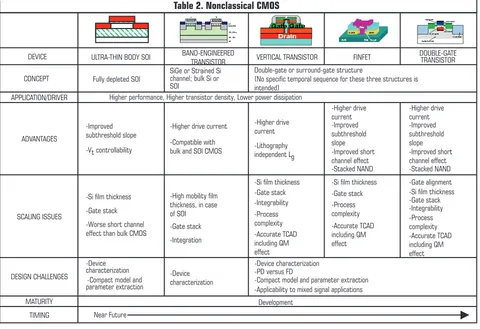
The industry is pursuing two fundamentally distinct ap-proaches to managing these scaling challenges—bulk transis-tors enhanced using new materials for the gate stack, etc., and new transistor structures. Zeitzoff and Chung discuss process methods related to bulk CMOS transistors in another article in this issue [8]. This article addresses methods related to introduc-tion of structural changes to the MOSFET. These structural changes are compared in Table 2 and discussed below.
Nonclassical CMOS structures includes those advanced MOSFETs that provide a path to scaling CMOS to the end of the time horizon of the 2001 Roadmap using new transistor struc-tural designs. Nonclassical entries include ultra-thin-body SOI, the band-engineered transistor, and three entries for double gate structures. Candidate structures are discussed briefly below.
The ultra-thin-body MOSFET [9, 10] consists of a fully de-pleted silicon-on-insulator (SOI) MOSFET with an ultra-thin body or channel (5-10-nm thick). Currently in production, to-day’s SOI CMOS transistor is a partially depleted MOSFET, where there is a quasi-neutral body or substrate region under all operating bias conditions. This quasi-neutral body is usually left floating with no external electrical connection. Alternatively, the quasi-neutral body is electrically connected to the source or to an externally accessible body contact. In contrast, a fully de-pleted SOI CMOS transistor has no quasi-neutral body region because the entire body or substrate region is depleted of mobile carriers under all operating bias conditions. Electrical
connec-Table 2. Nonclassical CMOS
DEVICE ULTRA-THIN BODY SOI BAND-ENGINEERED
TRANSISTOR VERTICAL TRANSISTOR FINFET
DOUBLE-GATE TRANSISTOR
CONCEPT Fully depleted SOI
SiGe or Strained Si channel; bulk Si or SOI
Double-gate or surround-gate structure
(No specific temporal sequence for these three structures is intended)
APPLICATION/DRIVER Higher performance, Higher transistor density, Lower power dissipation
ADVANTAGES bulk and SOI CMOS
-Higher drive effect than bulk CMOS
-High mobility film
characterization -Device characterization-PD versus FD
-Compact model and parameter extraction -Applicability to mixed signal applications
MATURITY Development
tion to the body is not possible. Ultra-thin body scaling provides the extremely thin channel dimensions required to scale CMOS to the 22 nm node. Recently a new structure has been reported [10] utilizing a thin Si channel (5–20 nm) isolated from the sub-strate by a thin localized buried dielectric layer (10–30 nm). This structure combines the best features of bulk CMOS (e.g., deep source/drain regions) with the best features of SOI (e.g., ultra-thin channel and dielectric insulating layer).
The concept of a band-engineered transistor [11-13] is to en-hance the mobility of electrons and/or holes in the channel by modifying the band structure of silicon in the channel in a way such that the physical structure of the transistor remains sub-stantially unchanged. This enhanced mobility increases the tran-sistorgmandIon.A Si-Ge layer or a strained-silicon on relaxed
Si-Ge layer is used as the enhanced-mobility channel layer. The device structure can be a bulk transistor or an SOI transistor.
A vertical transistor [14] is one having surface conduction channels on two or more vertical surfaces and having current flow in the vertical direction. The channel length is given by the vertical separation between source and drain, which is usually determined by the thickness of an epitaxial layer and not by a lithographic step
A FinFET [15] is another form of a double gate transistor hav-ing surface conduction channels on two opposite vertical sur-faces and having current flow in the horizontal direction. The channel length is given by the horizontal separation between
source and drain and is usually determined by a lithographic step combined with a side-wall spacer etch process
A double-gate transistor [16] is one having surface conduc-tion channels on two opposite horizontal surfaces and having current flow in the horizontal direction. The channel length is given by the horizontal separation between source and drain and is defined by a lithographic step combined with an etch process.
Memory Devices
An important feature of silicon CMOS technology is the integrity of CMOS switches; i.e., CMOS switches have allowed realization of both memory and logic devices. This integrity is a great advan-tage of CMOS technology, though not without some inherent drawbacks. For example, CMOS memory technology (e.g., DRAM or SRAM) did not offer a solution for nonvolatile RAM.
In the post-CMOS era, most probably there will be two sepa-rate paths for development of memory and logic devices (see, for example, Fig. 2).
General expectations for post-CMOS memories can be sum-marized as nonvolatile, fast, low energy, and high density. Ideally, we need technologies that will combine higher density with the fast read/write speeds of synchronous RAM, the lower cost of dynamic RAM, and the nonvolatility of flash memory, which can store data when a device is turned off. Another critical issue is the scalabilityof a given memory technology—how many generations will a chosen technology survive?
SET Molecular
RSFQ Molecular
CNN Architecture
Non-classical
CMOS Memory
Logic
Time Strained Si
Vertical
Transistor FinFET
Planar Double Gate Phase
Change Nano FG
Magnetic RAM
SET QCA
RTD-FET
Quantum Computing Defect
Tolerant QCA
3-D Integration
FD SOI
Molecular
Emerging Technology
Vectors
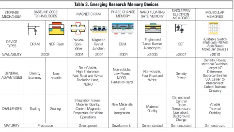
A summary of published research efforts on several memory technologies is shown in Table 3. As can be seen, existing research efforts are exploring a variety of basic memory mechanisms. These mechanisms include charge isolated by surrounding di-electrics, charge held in place by Coulomb blockade potential, chemical phenomena, magnetic phenomena, and material phase change. It is important to note that most of these memory options are thought to merge into a CMOS technology platform. Fabrica-tion is viewed as some type of modificaFabrica-tion or addiFabrica-tion to a CMOS platform technology. In Table 3, the parameters of emerging re-search memory devices are compared with current DRAM and Flash NOR technologies as benchmarks. DRAM and Flash NOR are the current dominant volume produced memories.
Potentially, the nearest term emerging memory technolo-gies are magnetic RAM and phase change RAM. One of the major drivers for both of these technologies isnonvolatility.
Magnetic RAMs (MRAM) [17] are based on the magnetoresis-tive effects in magnetic materials and structures that exhibit a re-sistance change when an external magnetic field is applied. In the MRAM, data are stored by applying magnetic fields that cause magnetic materials to be magnetized into one of two possible magnetic states. Reading data is performed by measuring resis-tance changes in the cell compared to a reference. Passing cur-rents nearby or through the magnetic structure creates the mag-netic fields applied to each cell. Two magnetoresistive effects are used in MRAM: giant magnetoresistance (GMR) and tunneling magnetoresistance (TMR). Correspondingly, two types of MRAM are explored: GMR (or its modified version pseudo spin valve—PSV) MRAM and magnetic tunnel junction (MTJ) MRAM. The PSV cell providing GMR is made of two magnetic layers (e.g., Ni, Co, Fe) separated by a thin conductive nonmagnetic layer (e.g.,
Cu). In PSV MRAM devices the GMR is sensed with the current flowing along the center conducting layer, which is coupled to both of the magnetic cladding layers. The resistance to current flow in the thin nonmagnetic conducting layer depends upon the alignment of magnetic spin polarization of each of the two clad-ding magnetic metal layers with each other and with the electrons in the center conducting layer. If the magnetic spins of the two magnetic cladding layers are aligned with each other, those elec-trons flowing in the center conducting layer that possess mag-netic spins aligned to these layers will experience little large angle scattering and will, therefore, flow with little resistance. If the magnetic spins of the two cladding magnetic layers are not aligned with each other, then the magnetic spins of all electrons in the center nonmagnetic conducting layer will be misaligned with one or both of the cladding layers. Consequently, for this case a fractionally larger resistance will impede current flow in the center nonmagnetic conducting layer. The difference between 0 and 1 levels corresponds to about 12% of the cell resistance. Dis-advantages of PSV cells: low impedance, small signal voltage dif-ference of±3 mV during a read operation resulting in larger read time. The MTJ cell is made of two ferromagnetic layers separated by a thin insulating layer that acts as a tunnel barrier. In contrast to giant magnetoresistive (GMR) structures in which the sense current usually flows parallel to the layers of the structure, the current is passed perpendicular to the layers of the MTJ sandwich. Similarly to GMR the resistance of the MTJ sandwich depends on the magnetic arrangement of the magnetic moments of the two ferromagnetic layers. Typically, the resistance of the MTJ is lowest when these moments are aligned parallel to one another, and it is highest when antiparallel, thereby giving rise to magnetoresis-tance. The read operation is performed by measuring
spin-de-Table 3. Emerging Research Memory Devices
STORAGE
TYPES DRAM NOR Flash
Pseudo-AVAILABILITY 2002 ~2004 ~2004 ~2004 >2005 >2007 >2010
GENERAL Fast Read and Write,
pendent tunneling current between the magnetic layers, thus the impedance is high and the difference between the 0 and 1 level can achieve 50% of cell resistance. Perhaps, the biggest problem of MRAM isscalability. The scalability of magnetic memory cells is difficult because the magnetic field needed for write operation is the same for smaller and larger memory cells. Since current pass-ing through the cell produces the magnetic field, the write cur-rent density increases for smaller cell size.
Phase change memory [18, 19], also called ovonic unified memory (OUM), is based on rapid reversible phase change effect in some materials under the influence of electric current pulses. The OUM uses the reversible structural phase-change in thin-film material (e.g., chalcogenides) as the data storage mechanism. The small volume of active media acts as a program-mable resistor between a high and low resistance with > 40X dy-namic range. Ones and zeros are represented by crystalline versus amorphous phase states of active material. Phase states are programmed by the application of a current pulse through a MOSFET which drives the memory cell into a high or low tance state, depending on current magnitude. Measuring resis-tance changes in the cell performs the function of reading data. OUM cells can be programmed to intermediate resistance val-ues; e.g., for multistate data storage.
The potential advantage of OUM is a relatively simple system based rather on “smart” material properties than on an elaborate multi-material layered structure. Also, since the energy re-quired for phase transformation decreases with cell size, the write current can scale with cell size (at least theoretically), thus facilitating memory scaling.
In this article, we will not consider a family of research mem-ory technologies often combined under name “single electron memory.” These technologies are very well represented in the fol-lowing references [20-28]. However, it is important to note that, in fact, there are two different technologies often referred as to single electron memory. Since the physical principle of operation of these two technologies is very different, the 2001 ITRS distin-guishes betweennanofloating gate memoryandsingle electron memory[29]. While the nanofloating gate memory includes sev-eral possible evolutions of conventional floating gate memory, the basic component of single-electron memory is the single-electron transistor. At this point, the time horizons of nanofloating-gate and single-electron memories are unclear, due to several impor-tant drawbacks. For example, a major drawback of nanofloating-gate memory is relatively low endurance (e.g., the number of erase/write cycles) [29]. Major disadvantages of all single-electron memories reported so far are volatility, very low operating tem-perature of 4.2-20 K and background charges [29].
The memory technology with likely the longest time horizon is molecular memory [30, 31]. Molecular memory is a broad term combining different proposals for using individual mole-cules as building blocks of memory cells in which one bit of in-formation can be stored in the space of an atom, molecule, or cell. One experimentally demonstrated approach is based on rapid reversible change of effective conductance of a molecule attached between two electrodes controlled by applied voltage.
In this molecular memory, data are stored by applying external voltage that causes the transition of the molecule into one of two possible conduction states. Data is read by measuring resistance changes in the molecular cell. There are also concepts for com-bining molecular components with current memory technol-ogy; e.g., DRAM and floating gate memory. In this case, the molecular element acts as a nano-sized resonant tunnel diode or ultimately small memory node. A major drawback of experimen-tally demonstrated approaches in molecular memory is their in-herent two-terminal nature. A number of advanced molecular components have been proposed, such as three-terminal molec-ular devices (molecmolec-ular transistor), molecmolec-ular NEMS, and spin-based molecular devices. While molecular memory perhaps represents the highest scalability, thenonvolatilityis a difficult challenge for molecular devices. At this point, no nonvolatile molecular memory has been demonstrated.
Application-Specific Emerging Technologies
As discussed above in the section on “Emerging Technology Parametrization,” many of the emerging information and signal processing technologies address particular domains of applica-tion, defined by their density, speed, size, and cost, and these do-mains likely are not attainable by silicon CMOS. This suggests two thoughts. First, these new approaches could possibly extend the applications of microelectronics to domains and products currently not within the reach of silicon CMOS. Second, silicon CMOS and related memory technologies will undoubtedly be in-tegrated with these new technologies to serve far beyond their scaling time horizon as systems integrating platforms. The sec-tions below discuss some of the candidate concepts.
Logic Devices
Different from memory technologies, which are thought to be universal in their applications, the beyond-CMOS solutions to logic devices probably will be more application specific. Another important difference between potential beyond-CMOS memory and logic is that while the memory options are thought to merge into a CMOS technology platform, such integration could be more difficult for logic devices. A summary of published re-search efforts on several emerging logic technologies is shown in Table 4.
Similar to memory devices, the new logic technologies must meet certain fundamental requirements and possess certain compelling attributes to justify the very substantial investments that will be necessary to build a new infrastructure. First and foremost, any new information-processing technology must sat-isfy the following requirements:
✦ Functionally scaleable well beyond (>100X) CMOS; ✦ High information/signal processing rate and throughput;
✦ Minimum energy per functional operation;
✦ Minimum scaleable cost per function.
transmis-sion of flux quanta defines the device operation. The basic RSFQ structure is a superconducting ring that contains one Josephson junction plus an external resistive shunt. The storage element is the superconducting inductive ring and the switching element is the Josephson junction. RFSQ dynamic logic uses the pres-ence or abspres-ence of the flux quanta in the closed superconducting inductive loop to represent a bit as a “1” or “0,” respectively. The circuit operates by temporarily closing the Josephson junction, thereby ejecting the stored flux quanta. When that happens, a quantized voltage pulse is generated across the Josephson junc-tion. This voltage pulse is propagated down a superconducting transmission line and can be used to trigger other RSFQ struc-tures in various combinations to form complex circuits. As this quantum effect occurs at a macroscopic scale, sub-micron li-thography is not a prerequisite. With RSFQ, circuit speeds above 100 GHz (perhaps up to 750 GHz) are possible. RSFQ circuits are currently built on low-temperature superconducting Josephson Junctions (~5 K) and high-temperature superconductors may eventually be exploited. RSFQ devices need extreme cooling be-cause the device operating temperature is lower than the critical temperature of the bulk superconductor material. The availabil-ity of adequate cooling systems, which comply with needed specifications (temperature, size, weight, dimensions, etc.) in the limits of reasonable prices, is one of the most important drawbacks for the market introduction of this technology. An-other difficult problem of RSFQ is scalability: the minimum critical dimension is limited by magnetic penetration depth.
According to estimates [2], for Nb-based low-temperature su-perconductors, the minimum size will be 100 nm, while for high-temperature superconductors, the minimal feature size is about 500 nm. Thus, high-scale integration is one of major challenges of RSFQ devices.
When one thinks of a universal beyond-CMOS technology, molecular electronics is perhaps first in the list of choices. A hypo-thetical ability to make both molecular memory and molecular logic would, in principle, build a new platform to replace the sili-con platform. However, at this point the feasibility of such a uni-versal molecular platform for future nanoelectronics is unclear. Molecular logic devices are based on electron transport prop-erties through a single molecule [33]. Experimental demonstra-tions to date have been performed using two-terminal molecular devices [34], although three-terminal molecular structures have been proposed [35], and one has been recently demonstrated [36]. Two-terminal molecular devices currently being explored consist of thousands of molecules operating in parallel; e.g., as digital switches or as analog diodes. In both cases a voltage ap-plied to a group of parallel molecules results in reconfiguration of the molecular components, or moieties, and a change in the molecule’s electrical conduction properties [34, 37]. The mech-anism of charge transport in molecules is not understood. One possible model is this change in a molecule’s electrical proper-ties is caused by a change in the overlap of the orbitals in the molecule. The correct overlap of the molecular orbitals allows electrons to flow through the molecule. But when this overlap of
Table 4. Emerging Logic Devices
DEVICE
Demonstrated Demonstrated Demonstrated Demonstrated
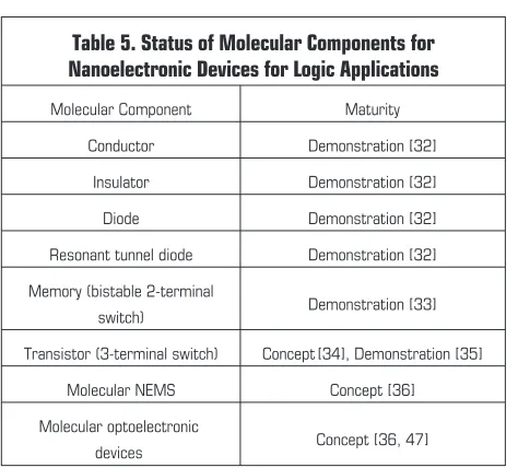
orbitals is further changed (because the molecule has been twisted or its geometry has been otherwise changed) the flow of electrons is impeded. A near term opportunity of molecular elec-tronics is in integration of molecular components with sub-100 nm CMOS [38] to form hybrid systems. Potential longer-term opportunities are full-molecular systems. In addition to two-ter-minal digital switches and analog diodes, several other molecu-lar components have been recently studied both experimentally and theoretically; e.g., bistable switch, molecular NEMS, three-terminal molecular devices (molecular transistor), and spin-based molecular devices. A brief summary of the status of
exploration (maturity) of molecular components for nanoelectronics is given in Table 5.
A special and important subset of molecular electronic mate-rials is carbon nanotubes [39]. A carbon nanotube is a molecular “tube” or cylinder formed from an atomic “sheet” of carbon at-oms. These carbon atoms are bonded together into an array of hexagons, which form a planar sheet, similar to an atomic sheet of graphite (and looking like a section of chicken wire). This graphite-like (graphene) sheet is rolled up to form a carbon nanotube. Carbon nanotubes can have diameters between 1–20-nm and lengths from 100-nm to several microns. The tube diameter and just how the sheet of carbon hexagons is rolled up determine whether a tube is a semiconductor or a metal. If a tube is a semiconductor, the details of rolling also determine the en-ergy bandgap and, therefore, the electronic properties of the tube. These bandgap energies range all the way from zero (like a metal) to values as large as silicon, with many values in between. The tubes can be doped both p- and n-type, making possible p-n junctions. Several groups have demonstrated p-FET device structures in which a gate electrode modulates the conductivity of a conducting channel by a factor of 105or more, similar to sili-con MOSFETs [40]. Large arrays of carbon nanotube FETs have been fabricated [41] and, more recently, a voltage inverter or NOT gate circuit using one n-channel and one p-channel FET was demonstrated [42].
Architectures
The Merriam Webster dictionary [43] defines computer architec-ture as “the manner in which the components of a computer or computer system are organized and integrated.” The previous
sec-N O2
HN2
Table 6. Emerging Research Architectures
ARCHITECTURES
MATURITY Demonstration Demonstration Demonstration Concept Demonstration Concept
Table 5. Status of Molecular Components for Nanoelectronic Devices for Logic Applications
Conductor Demonstration [32]
Insulator Demonstration [32]
Diode Demonstration [32]
Resonant tunnel diode Demonstration [32]
Memory (bistable 2-terminal
switch) Demonstration [33]
Transistor (3-terminal switch) Concept [34], Demonstration [35]
Molecular NEMS Concept [36]
Molecular optoelectronic
tions of this article have discussed the anticipated evolution of the compo-nents themselves but have not dealt with organiza-tion or integraorganiza-tion; i.e., the architecture of those com-ponents. This section will address new architectural methodologies that are likely to emerge in the next few years to bring
the component technologies to new systems applications. Two principal forces are driving research into new systems architectures. One is the invention of devices and technologies embodying completely new physical principles of operation be-yond the FET (e.g., molecular electronics and quantum cellular automata). These new structures are not plug-to-plug compati-ble with existing MOSFETs and will require new architectures to achieve useful functionality. Thus, the development of new de-vices can be thought of as driving the development of new archi-tectures necessary to support their application.
The second force is the development of new processing tech-nologies combining CMOS functions (such as logic, memory, etc.) with each other and with other functions (RF, analog, opti-cal, MEMS, etc.). Development of advanced wafer bonding tech-niques is driving consideration of 3-D integration of silicon devices and the requirement for new systems architectures. Similarly, the development of optical input/output with broad bandwidth capability may drive a new architecture that would exploit that capability. Thus, development of new processes may be thought of as enabling new architectures that were not previ-ously possible. Table 6 outlines some of the emerging research architectures currently on the horizon.
The first entry in Table 6 is heterogeneous 3-D integration. It is one of the central technologies necessary to implement the vi-sion presented in the first section of this article. As stated earlier, emerging technologies beyond scaled CMOS offer the potential for greatly improved performance by mixing and matching tech-nologies for particular applications, perhaps integrated with CMOS logic and memory platform technologies to provide sys-tem backbone functions. Effective combination of technologies requires 3-D integration of various functionally dissimilar tech-nologies beginning with microprocessors, ASICs, DRAMs, and extending to RF, analog, optical, and MEMS. These dissimilar technologies may later include 3-D integration of molecular, plastic, RSFQs, and others directly onto silicon platforms. In some instances, such as RSFQs, the integration involves mixing two completely different principles of information coding (one is electric charge and the other is magnetic flux quanta)
Another motivation for 3-D integration is related to improv-ing the performance of CMOS systems as the devices continue to scale down in size. The device performance is expected to scale faster than performance of global interconnect, leading to a situ-ation in which the overall system performance is dominated by
global interconnect la-tency. It has been shown that 3-D superposition of devices can decrease interconnect delays by up to 60% relative to an equivalent number of transistors arranged in a planar arrangement and is therefore one method of address interconnect delay [44, 45].
Three-dimensional integration can be achieved by either low-temperature wafer bonding or integrated process flows on a common substrate. Integrating process flows may work for rela-tively similar technologies but will not work for radically differ-ent technologies. For those, low-temperature wafer bonding will be necessary, typically at temperatures less than 200°C in order not to affect the materials and structures fabricated in previous processing steps.
The second architecture shown in Table 6 is quantum cel-lular automata, which is quite different from the von Neumann architecture common to CMOS-based micropro-cessors. The QCA paradigm is differentiated by the locality of interaction in which each cell talks only with its nearest neighbors and the fact that the communication occurs via electromagnetic fields and quantum tunneling rather than charge flow in a conductor.
If QCA cells are arranged in a regular square grid, then long-established cellular automata theory can be applied to-gether with cellular nonlinear (or neural) network (CNN) theory to describe the information-processing algorithm. This allows a large body of theory and the corresponding algorithms to be ap-plied directly to QCA architectures. Regular QCA grids are very efficient at solving of diffusion and wave equations [46], image processing, and neural system simulation. It is also possible to construct a complete set of Boolean gates that are moderately ef-ficient by departing from the requirement that the grid be regu-lar and designing custom celluregu-lar configurations for the different Boolean gates.
QCA operation can be improved by introducing an “adiabatic clocking field,” which controls the switching of the cells and al-lows them to evolve relatively rapidly to a stable end state. This clock has the additional advantage that it effectively produces gain, nonlinearity, and isolation between neighboring parts of a circuit. Recent experimental results [46] have confirmed the original theory. Using clocking adds to the complexity of pure QCA circuits but greatly extends their possible range of applica-tions. Device and circuit analyses indicate that the speed of QCA circuits will be limited to by the time required to raise and lower potential barriers between adjacent cells.
The third and forth entries in Table 6 are closely linked and any discussion of molecular architecture requires first a discus-sion of defect-tolerant architecture [47].Defect-tolerant com-puter architecture implies that a system operates satisfactory in
The need for defect-tolerant hardware
emerges from the possibility of
fabricating nanometer-scale elements that
will probably not satisfy tolerance
and reliability requirements that are
the presence of errors made in the hardware during manufacture. This is different from fault tolerance, which implies the ability of a m a c h i n e t o r e c o v e r from errors made dur-ing a calculation. The need for defect-tolerant
hardware emerges from the possibility of fabricating nanometer-scale elements that will probably not satisfy toler-ance and reliability requirements that are typical for larger scale systems. Systems consisting of molecular-size components are likely to have many imperfections, and a computing system de-signed on conventional zero-defect basis would not work.
For a conventional integrated circuit, a description of the chip function is first developed, and then the hardware is con-structed. The general idea behind defect-tolerant architectures is conceptually the opposite. A generic set of wires and switches are fabricated, and then the resources are configured by setting switches linking them together to obtain the desired functional-ity [47]. A cornerstone of defect-tolerant systems is redundancy of hardware resources, thus extra components such as switches, memory cells, and wires are needed. This redundancy in turn implies very high integration density. The fabrication could be very inexpensive (e.g., the limit case would be chemical self-as-sembly of molecular switches on a three-dimensional random array of wires). However, to make such a circuit operational, a la-borious process of testing is needed when the devices are trained to the desired level of proficiency with computer tutors that find the defects and record their locations in on-chip databases [47]. In principle not only information on defects, but also all answers to the input questions (such as all logic functions), can be put into memory cells, provided there is adequate amount of fast-ac-cess memory. On the other hand, to deal with defective ele-ments, an opportunity for rerouting the data flows in hardware should exist. This implies spare wires to provide a large commu-nications bandwidth. Such a “memory and wires” approach to computation, while very challenging, may be realized in molec-ular computers.
The main two potential advantages of defect-tolerant archi-tectures are as follows:
✦ The possibility of building complex systems from
inher-ently imperfect nanoscale components.
✦ The potential for self-repair from operation-originated
de-fects by reconfiguring the system.
An important disadvantage of defect-tolerant computing is the need for a laborious post-fabrication learning process. Also, very large amounts of wiring and spare devices may be needed to cope with relatively high defect rates. However, defect-tolerant architecture is a broad concept, which can be realized with dif-ferent approaches, for example in a memory-based molecular computer or with cellular nonlinear networks.
As mentioned above, defect-tolerant architec-ture is one of the en-abling technologies for molecular architecture.
Even though three-ter-minal molecular devices with gain have recently been demonstrated [36], the extremely demand-ing interconnect requirements required for three-terminal op-eration dictate that molecular architecture will probably be memory based. The logic functions will consist of precalculated truth tables stored in memory and accessed via dense self-assem-bled interconnect fabrics.
Cellular nonlinear networks [48, 49] executed in tunneling phase logic (CNN/TPL)[50] and quantum computing [4, 51-58] are both radically new technologies and architectures that will not be discussed in detail except to note that they implement two alternative forms of phase logic. CNN/TPL encodes information as the phase of an electrical signal relative to the phase of a reference signal. Quantum computing encodes information in the relative phase and amplitudes of the wavefunctions of entangled qubits.
Emerging Technology Sequence
The preceding sections have surveyed the universe of emerging research devices, introduced a parametrization scheme to relate them to each other and to scaled CMOS, and discussed individual device and architectural concepts. The emerging research de-vice parametrization shown in Fig. 1 summarizes that informa-tion at some future point in time but contains no informainforma-tion on the evolutionary sequence required to reach that point. The in-dividual tables on logic, memory, and architectures do contain some limited sequence information and show time increasing from left to right. However, no attempt has been made to address the global evolutionary sequences that are likely to appear and dominate our future technology.
The emerging technology sequence chart shown as Fig. 2 be-low is an attempt to create a relevant taxonomy that might char-acterize future development. The dominant feature of the chart below is the four parallel technology vectors. These technology vectors are identified as nonclassical CMOS, memory, logic, and architecture. These vectors may not be the right ones or even the right number, but they illustrate two very important points about the nature of future microelectronic development. First, microelectronics development will continue along a finite num-ber of well-defined evolutionary pathways that permit incre-mental change in existing devices to produce dramatic improvements in systems performance. The process of changing one thing at a time while holding everything else constant has served the microelectronics industry very well and it is not likely to be abandoned. It permits detailed planning with well-defined roadmaps and leads to an inherently efficient process. It is the foundation on which the ITRS process is based and it will
con-The process of changing one thing at a time
while holding everything else constant has
served the microelectronics industry very well,
tinue, although there will be some diversifica-tion in the tradidiversifica-tional sequences as shown in Fig. 2.
The second point is closely related to the first—emerging tech-nologies and architec-tures will establish their own evolutionary
pro-gressions. This means that they will not be extensions of the cur-rent sequences. More importantly, after initial research demonstrates their function and application-driven potential, their subsequent development usually will likely occur as an or-derly progression. One aspect of current research in emerging technologies is the seemingly random way in which new discov-eries are announced in one emerging area with no relationship to other emerging technologies. As powerful as this process is to the creation of paradigm-shifting approaches, this also is alien to the operational mode of the microelectronics industry, creates distrust of the emerging technologies, and impedes their even-tual adoption.
It is important to understand that the time scale for each technology vector is independent of the other technology vec-tors. Thus, vertical alignment of technologies is not meant to imply synchronicity of the technologies. For example, quantum computing will certainly be here very much later than double-gate transistors
The bottom vector in Fig. 2 is labeled nonclassical CMOS and is an extension of the existing ITRS roadmap. The first two entries in that vector are fully depleted SOI devices and strained silicon (or some other form of mobility enhancement material or struc-ture). These are listed first because the operational principles are well understood, as are some of the manufacturing issues. The last three entries on this vector are various forms of double-gate de-vices. The industry likely will settle on one of these devices once all the manufacturing issues are understood, and the other two will not be pursued to any extent. Currently, a clear winner of the three-candidate double-gate devices has not emerged.
The second vector labeled memory is also a continuation of the existing memory roadmap. The first entry in that vector is magnetic RAM, which is in limited production now and will clearly precede the other entries. The second entry is phase-change memory, which is in an advanced state of develop-ment and may be expected in high volume manufacture rela-tively soon after MRAM memories. The next entry is nanofloating gate memory, which will likely be the next major advance. It operates by embedding nanocrystals in the gate of a CMOS device and can be manufactured without developing addi-tional underlying technologies. The order of the last two entries is somewhat speculative because they depend on development of new underlying technologies. The SET device will need cryo-genic cooling of some kind and the molecular memory will re-quire a new interconnect technology. Development of the last
two memory devices will be gated by the advance-ment of the underlying technologies.
Each of the concepts for new forms of a logic technology is highly speculative. For this reason, placement of these concepts on the logic technology vector is very uncertain and is meant to be illustrative and not predic-tive. The RTD/MOSFET gate is simply the combination of two w e l l - k n o w n d e v i c e s t o f o r m a n e w m u l t i v a l u e d , multifunctional gate. This new RTD/MOSFET gate could re-duce the parts count and power dissipation and increase the speed of some applications by factors of two to four. Examples of applications include SRAM cell, latched comparators, shift registers, etc. One major issue is development and manufacturability of a silicon-based RTD integrated with MOSFETs, and the other is whether the potential advance would justify major costs for R&D and for manufacturing re-tooling. The SET logic device depends on cryogenic cooling as an enabling technology as do RSFQs. Development of QCA for logic applications depends on the supporting architecture and cryogenic cooling. Molecular logic devices depend on develop-ment of a three-terminal device and an interconnect technology. The emerging architectures technology vector is fundamen-tally different compared to the other three. Each of the emerging architectures is completely different and independent of the oth-ers. For this reason it is much more difficult to suggest a sequen-tial development of new architectures. As with the logic vector, placement of the emerging architectures is highly speculative and meant to be more illustrative and not predictive. Three-di-mensional heterogeneous integration of discrete chips and wa-fers likely will occur in the near term for three reasons. Most of the requisite technology is available, manufacturing tools are emerging, and lastly market applications are driving this tech-nology. Beyond that, QCA or, more generally, field-coupled ar-chitectures will probably be next although that is open to question. Defect-tolerant architectures are closely coupled to molecular computing architectures and those will have to occur in parallel. The development of molecular architectures will of course be gated by molecular devices which in turn is gated by interconnect issues. Cellular nonlinear networks are shown next and they are gated by a host of underlying technologies includ-ing phase logic, quantum RTDs, cryogenics, and probably oth-ers. The last architecture is undoubtedly quantum computing, which will be gated by invention and reduction to manufactur-ing of a practical, affordable solid-state machine.
Successful development of the multitude of technologies shown in Fig. 2 will require a stable integrating platform to merge the new technologies with a stable infrastructure tech-nology providing backbone integration and data-storage func-tions. That platform undoubtedly will be scaled silicon,
A successful new information-processing
paradigm most likely will require a new
platform technology embodying a
fabric of interconnected primitive logic
combined with a relevant memory technology. This scenario points to the benefits of heterogeneous integration of comple-mentary technologies discussed in this article.
Summary and Conclusions
The accelerating pace of CMOS scaling is rapidly approaching the fundamental limits of MOSFET performance, even as the projected size of a high-performance and manufacturable MOSFET technology is currently being extended with growing confidence to the 22-nm node (featuring a 9-nm physical gate length). The new 2001 International Technology Roadmap for Semiconductors currently projects the industry to reach this node in 2016. However, this forecast assumes the traditional in-dustry node-cycle cadence of a quadrupling of the number of transistors every three years for DRAMs and a return to the three-year cycle in 2004 for MPUs and ASICs. During the past several years the node cycles for MPUs have been accelerated to occur within two-year periods. This pace will bring the micro-electronics industry to the end of silicon CMOS technology scal-ing sometime not later than 2016, and maybe as soon as 2010.
The new Emerging Technologies section of the 2001 ITRS of-fers guidance on both sides of this problem. The first discusses approaches to nonclassical MOSFET structures that may facili-tate a high-performance, manufacturable CMOS technology reaching the 22-nm node, and the second reviews many new ap-proaches to information and signal processing proposed to ex-tend microelectronics far beyond the end of CMOS scaling. Review of nonclassical MOSFET structures includes ul-tra-thin-body and channel-engineered MOSFET structures to-gether with three varieties of double-gate MOSFET structures. Development of these and other nonclassical CMOS structures is aimed at attacking the scaling problem from a structural per-spective. This will complement the intense efforts to improve conventional bulk MOSFETs to reach the 22-nm node through introduction of new materials for the gate stack (high-K gate di-electric, metal gate electrodes, etc.).
This review of many new information and signal processing paradigms for the time horizon beyond that of the 2001 ITRS necessarily includes both device technologies and systems ar-chitectures. Rather than replacing CMOS, one or more of these embryonic paradigms,when combined with a CMOS platform,
could extend microelectronics to new applications domains cur-rently not accessible to CMOS. A successful new informa-tion-processing paradigm most likely will require a new platform technology embodying a fabric of interconnected primitive logic cells, perhaps in three dimensions. Further, this new logic paradigm may suggest a new symbiotic informa-tion-processing architecture to fully extract the potential of-fered by the logic fabric. Consequently, discovery and development of a new industry-shifting information- and sig-nal-processing paradigm may greatly benefit from close collabo-ration between device technologists and systems architects.
James A. Hutchbyis with Semiconductor Research Corp. in Dur-ham, North Carolina (e-mail: [email protected]). George I.
Bourianoffis with Intel Corp. in Hillsboro, Oregon.Victor V. Zhirnov
is with N.C. State University in Raleigh, North Carolina.Joe E. Breweris with the University of Florida in Gainesville, Florida.
References/Endnotes
[1] Semiconductor Industry Association (SIA),International Roadmap for Semiconductors 2001 edition, Austin, TX: International SEMATECH, 2001. Available: http://public.itrs.net
[2] R. Compano, Ed.,Technology Roadmap for Nanoelectronics, 2nd ed., Nov. 2000.
[3] Research Triangle Institute, Technology Assisted Learning Division (Ms. P.J. Woodard, Mr. Sam Field, and Mr. Dale Rowe) is gratefully acknowl-edged for providing technical support in the preparation of Fig. 1.
[4] P.W. Shor, “Algorithms for quantum computation: Discrete logarithms and factoring,” inProc. 35th Annu. Symp. Foundations of Computer Sci-ence,1994, pp. 124-134.
[5] Estimated on the principle of reasonable cost and assumed a two-dimen-sional architecture of NEMS computer.
[6] M. Despont, J. Brugger, U. Drechsler, U. Düring, W. Haberle, M. Lutwyche, H. Rothuizen, R. Stutz, R. Widmer, G. Binnig, H. Rohrer, P. Vettiger, “VLSI-NEMS chip for parallel AFM data storage,”Sensors Actuat.,vol. 80, pp. 100-107, 2000.
[7] H-S.P. Wong, P.M. Soloman, J.J. Welser, “Nanoscale CMOS,”Proc. IEEE, vol. 87, pp. 537-590, 1999.
[8] P.M. Zeitzoff and J. Chung, “Weighing in on digital logic scaling trends,” IEEE Circuits Devices Mag., vol. 18, pp. 18-27, Mar. 2002.
[9] S. Cristoloveanu, “SOI technology: Renaissance or science fiction?” in Fu-ture Trends in Microelectronics, S. Luryi, J. Xu, and A. Zaslavsky, Eds. New York: Wiley, 1999, pp. 105-114.
[10] M. Jurczak, T. Skotnicki, M. Paoli, B. Tormen, J. Martins, J. Regolini, D. Dutartre, P. Ribot, D. Lenoble, R. Pantel, and S. Monfray, “Silicon-on-Noth-ing (SON)—An innovative process for advanced CMOS,”IEEE Trans. Elect. Dev.vol. 47, p. 2179, 2000.
[11] R. Hartmann, U. Gennser, H. Sigg, D. Grützmacher, and G. Dehlinger, “Si/SiGeC Heterostructures: A path towards high mobility channels,” in Future Trends in Microelectronics,S. Luryi, J. Xu, and A. Zaslavsky, Eds. New York: Wiley, 1999, pp. 133-141.
[12] J. Alieu, T. Skotnicki, P. Bouillon, J.L. Regollini, A. Souifi, G. Guillot, and G. Bremond, “Potential of SiGe-Channel MOSFETs for a submicron CMOS technology,” in Future Trends in Microelectronics, S. Luryi, J. Xu, and A. Zaslavsky, Eds. New York: Wiley, 1999, pp. 143-153.
[13] S. Takagi, T. Mizuno, N. Sugiyama, T. Tezuka, A. Kurobe, “Strained-Si-on-insulator (strained-SOI) MOSFETs—Concept, structures, and device characteristics,” IEICE Trans. Electronicsvol. E84C, pp. 1043-1050. 2001.
[14] S-H. Oh, J.M. Hergenrother, T. Nigam, D. Monroe, F.P. Klemens, A. Kornblit, W.M. Mansfield, M.R. Baker, D.L. Barr, F.H. Baumann, K.J. Bolan, T. Boone, N.A. Ciampa, R.A. Cirelli, D.J. Eaglesham, E.J. Ferry, A.T. Fiory, J. Frackoviak, J.P. Garno, H.J. Gossmann, J.L. Grazul, M.L. Green, S.J. Hillenius, R.W. Johnson, R.C. Keller, C.A. King, R.N. Kleiman, J.T.-C. Lee, J.F. Miner, M.D. Morris, C.S. Rafferty, J.M. Rosamilia, K. Short, T.W. Sorsch, A.G. Timko, G.R. Weber, G.D. Wilk, and J.D. Plummer, “50-nm Ver-tical Replacement-Gate (VRG) pMOSFETs,” inIEDM Tech. Dig., 2000, p. 65.
[15] D. Hisamoto, W.C. Lee, J. Kedzierski, H. Takeuchi, K. Asano, C. Kuo, E. Anderson, T.J. King, J. Bokor, C.M. Hu, “FinFET—A self-aligned dou-ble-gate MOSFET scalable to 20 nm,”IEEE Trans. Electron. Dev.,vol. 47, pp. 2320-2325, 2000.
[16] F. Allibert, T. Ernst, J. Pretet, N. Hefyene, C. Perret, A. Zaslavsky, S. Cristoloveanu, “From SOI materials to innovative devices,”Solid State Electron.,vol. 45, pp. 559-566, 2001.
[18] T. Lowrey, “Ovonic unified memory.” [Online] Available: http://www.ovonic.com
[19] W. Wade and D. Lammers, “Intel grooms pair of substitutes for flash,”EE Times, p. 14, July 16, 2001.
[20] K.K. Likharev, “Layered tunnel barriers for nonvolatile memory de-vices,”Appl. Phys. Lett.vol. 73, pp. 2137-2139, 1998.
[21] K. Nakazato, K. Itoh, H. Mizuta, and H. Ahmed, “Silicon stacked tunnel transistor for high-speed and high-density random access memory gain cells,”Electronics Lett., vol. 35, pp. 848-850, 1999.
[22] S. Tiwari, J.A. Wahl, H. Silva, F. Rana, and J.J. Welser, “A silicon nanocrystals based memory,”Appl. Phys. Lett., vol. 68 pp. 1377-1379, 1996.
[23] X. Tang, X. Baie, J.P. Colinge, A. Crahay, B. Katschmarsyj, V. Scheuren, D. Spote, N. Reckinger, F. Van de Wiele, and V. Bayot, “Self-aligned sili-con-on-insulator nano flash memory device,”Solid-State Electron.,vol. 44, pp. 2259-2264, 2000.
[24] S.M. Sze, “Evolution of nonvolatile semiconductor memory: From float-ing-gate concept to single-electron memory cell,” inFuture Trends in Mi-croelectronics, S. Luryi, J. Xu, and A. Zaslavsky, Eds., New York: Wiley, 1999, pp. 291-303.
[25] K. Yano, T. Ishii, T. Hashimotoi, F. Murai, and K. Seki, “Room-tempera-ture single-electron memory,”IEEE Trans. Electron Dev., vol. 41, pp. 1628-1638,,1994.
[26] K. Yano, T. Ishii, T. Sano, T. Mine, F. Murai, T. Hashimoto, T. Kobayashi, T. Kure, K. Seki, “Single-electron memory for giga-to-tera bit storage,”
Proc. IEEE,vol. 87, pp. 633-651, 1999.
[27] N.J. Stone and H. Ahmed, “Silicon single electron memory cell,”Appl. Phys. Lett.,vol. 73,pp. 2134-2136, 1998.
[28] H. Mizuta, H.-O. Müller, K. Tsukagoshi, D. Williams, Z. Durrani, A. Irvine, G. Evans, S. Amakawa, K. Nakazoto, and Haroon Ahmed, “ N a n o s c a l e c o u l o m b b l o c k a d e m e m o r y a n d l o g i c d e v i c e s , ”
Nanotechnologyvol. 12, pp. 155-159, 2001.
[29] Semiconductor Industry Association (SIA),International Roadmap for Semiconductors 2001 edition, Austin, TX: International SEMATECH, 2001. Available: http://public.itrs.net
[30] M.A. Reed, J. Chen, A.M. Rawlett, D.W. Price, and J.M. Tour, “Molecular random access memory cell,”Appl. Phys. Lett., vol. 78, pp. 3735-3737, 2001.
[31] J. Berg, S. Bengtsson, P. Lundgren, “Can molecular resonant tunneling diodes be used for a local refresh if DRAM memory cells?”Solid-State Elec-tron.,vol. 44, pp. 2247-2252, 2000.
[32] D.K. Block, E.K. Track and J.M. Rowell, “Superconducting ICs: the 100 GHz second generation,”IEEE Spectrum,vol. 37,pp. 40-46, 2000.
[33] J.C. Ellenbogen and J.C. Love, “Architectures for molecular electronic computers: 1. Logic structures and an adder designed from molecular elec-tronic diodes,”Proc. IEEE, vol. 88, pp. 386-425, 2000.
[34] M.A. Reed, J. Chen, A.M. Rawlett, D.W. Price, and J.M. Tour, “Molecular random access memory cell,”Appl. Phys. Lett.vol. 78, pp. 3735-3737, 2001.
[35] E. Emberly and G. Kirczenov, “Principles for the design and operation of a molecular wire transistor,”J. Appl. Phys., vol. 88 pp. 5280-5282, 2000.
[36] J.H. Schon, H. Melig, and Z. Bao, “Field-effect modulation of the conduc-t a n c e o f s i n g l e m o l e c u l e s , ” S c i e n c e x p r e s s. A v a i l a b l e : www.sciencexpress.org/8 Nov. 2001, page 2.
[37] Y. Wada, “Prospects for single molecule information processing devices,”
Proc. IEEE, vol. 89, pp. 1147-1771, 2001.
[38] G.F. Cerofolini and G. Ferla, “Toward a hybrid micro-nanoelectronics,”
J. Nanoparticle Res.,to be published.
[39] P.G. Collins and P. Avouris, “Nanotubes for electronics,”Sci. Amer., pp. 62-69, Dec. 2000.
[40] R. Martel, T. Schmidt, H.R. Shea, T. Hertel, and P. Avouris, “Single- and multi-wall carbon nanotube field-effect transistors,”Appl. Phys. Letters,
vol. 73, pp. 2447, 1998.
[41] P.G. Collins, M. Arnold, and P. Avouris, “Engineering carbon nanotubes and nanotube circuits using electrical breakdown,”Science,vol. 292, p. 706, 2001.
[42] V. Derycke, R. Martel, J. Appenzeller, and P. Avouris, “Carbon nanotube inter- and intramolecular logic gates,”Nano Lett., vol. 1, no. 9, p. 453, 2001.
[43]Merriam-Webster Dictionary[Online]. Available: http://www.m-w.com/dic-tionary.htm.
[44] J.A. Davis, R. Venkatesan, A. Kaloyeros, M. Beylansky, S.I. Souri, K. Banerjee, K.C. Saraswat, A. Rahman, R. Reif, and J.D. Meindl, “Intercon-nect limits on gigascale integration (GSI) in the 21st century,”Proc. IEEE,
vol. 89, pp. 305-324, 2001.
[45] K. Banerjee, S.J. Souri, P. Kapur, and K.C. Saraswat, “3-D ICs: A novel chip design for improving deep-submicrometer interconnect performance and systems-on-chip integration,”Proc. IEEE,vol. 89, pp. 602-633, 2001.
[46] W. Porod et al., “Quantum-dot cellular automata: Computing with cou-pled quantum dots,”Int. J. Electron.vol. 86, pp. 549-590, 1999.
[47] J.R. Heath, P.J. Kuekes, G.S. Snider, R.S. Williams, “A defect-tolerant computer architecture: Opportunities for nanotechnology,”Science,vol. 280, pp. 1716-1721, 1998.
[48] L.O. Chua,CNN: A Paradigm for Complexity. Singapore: Word Scien-tific, 1998.
[49] In the literature, the abbreviation CNN is also used to indicate cellular neural networks. Cellular neural network architectures also satisfy condi-tions 1 and 2 above but differ from Cellular Nonlinear Networks in that Cel-lular Neural Networks allow only for linear interactions within and between cells. Consequently, Cellular Nonlinear Networks are capable of solving a more general class of problems
[50] T. Ohshima and R.A. Kiehl, “Operation of bistable phase-locked single-elec-tron tunneling logic elements,”J. Appl. Phys., vol. 80, pp. 912-923, July 1996.
[51] M. Steffen, L.M.K. Vandersypen, and I.L. Chuang, “Toward quantum computation: A five Qubit Quantum Processor,”IEEE Micro,vol. 21, no. 2, pp. 24-34, 2001.
[52] S. Takeuchi,“Experimental demonstration of a three-qubit quantum computation algorithm using a single photon and linear optics,”Phys. Rev., vol. 62, pp. 2301-2304, 2000.
[53] P. Grangier, G. Reymond, and N. Schlosser, “Implementations of quan-tum computing using cavity quanquan-tum electrodynamics,”Fortschr. Phys., vol. 48, pp. 859-874, 2000.
[54] C. Monroe, D.M. Meekhof, B.E. King, W.M. Itano, and D.J. Wineland, “Demonstration of a fundamental quantum logic gate,”Phys. Rev. Lett.
vol. 75, pp. 4714-4717, 1995.
[55] G.J. Milburn, “Quantum computing using a neutral atom optical lattice: An appraisal, ”Fortschr. Phys., vol. 48, pp. 957-964, 2000.
[56]] B.E. Kane, “A silicon-based nuclear spin quantum computer,”Nature, vol. 393, pp. 133-137, 1998.
[57] D.V. Averin, “Quantum computation and quantum coherence in mesoscopic Josephson junctions,” J. Low Temp. Phys. vol. 118, pp. 781-793, 2000.