Yevgeny Perelman
·
Ran Ginosar
The NeuroProcessor
An Integrated Interface to Biological
Neural Networks
Dr. Yevgeny Perelman
Technion-Israel Institute of Technology Dept. Electrical Engineering
32 000 Haifa Israel
Prof. Ran Ginosar
Technion - Israel Institute of Technology Dept. Electrical Engineering
32000 Haifa Israel
ISBN: 978-1-4020-8725-7 e-ISBN: 978-1-4020-8726-4
Library of Congress Control Number: 2008932564
c
2008 Springer Science+Business Media B.V.
No part of this work may be reproduced, stored in a retrieval system, or transmitted in any form or by any means, electronic, mechanical, photocopying, microfilming, recording or otherwise, without written permission from the Publisher, with the exception
of any material supplied specifically for the purpose of being entered
and executed on a computer system, for exclusive use by the purchaser of the work.
Contents
1 Introduction. . . 1
1.1 Overview of the Book . . . 3
2 Recording From Biological Neural Networks. . . 5
2.1 The Neuron . . . 5
2.1.1 The Membrane and Resting Potential . . . 6
2.1.2 Action Potential . . . 7
2.1.3 Excitation Propagation . . . 8
2.2 Interfacing Neurons Electrically . . . 10
2.2.1 Double Layer Capacitance . . . 10
2.2.2 Resistance at the Interface and Charge Transfer . . . 11
2.2.3 Diffusion Resistance Near DC . . . 12
2.2.4 AC Diffusion Resistance . . . 13
2.2.5 Electrode Noise . . . 14
2.3 Neuronal Probes for Extracellular Recording . . . 15
2.3.1 Penetrating Electrodes . . . 16
2.3.2 Cuff Electrodes and Regenerating Sieve Electrodes . . . . 17
2.4 Recording from Cultured Neural Networks . . . 17
2.4.1 MEAs on Silicon Substrate . . . 17
2.5 Typical Multi-Electrode Recording Setup . . . 18
2.6 Recorded Signal Information Content . . . 20
3 The Neuroprocessor . . . 23
3.1 Datarate Reduction in Neuronal Interfaces . . . 24
3.2 Neuroprocessor Overview . . . 24
4 Integrated Front-End for Neuronal Recording . . . 27
4.1 Background . . . 27
4.1.1 Blocking the DC Drifts . . . 27
4.2 NPR01: First Front-End Generation . . . 30
VI Contents
4.3.1 Splitting Spike and LFP . . . 31
4.3.2 NPR02Architecture . . . 32
4.3.3 Input Preamplifier . . . 34
4.3.4 NPR02Measurements . . . 35
5 NPR03: Mixed-Signal Integrated Front-End for Neuronal Recording . . . 39
5.1 Overview . . . 39
5.2 NPR03Architecture . . . 40
5.2.1 Chip Communications . . . 41
5.2.2 Instruction Set and Register Access . . . 42
5.3 Host Interface . . . 43
5.4 NPR03Channel . . . 44
5.5 Analog-to-Digital Converter . . . 44
5.6 Integrated Preamplifier With DC Blocking . . . 46
5.6.1 ChoosingCi andCf . . . 46
5.6.2 Noise Analysis . . . 47
5.6.3 Discussion . . . 51
5.7 NPR03Measurements . . . 52
5.8 An NPR03-Based Miniature Headstage . . . 53
5.9 A Novel Opamp for The Front-End Preamplifier . . . 58
5.9.1 Noise Analysis . . . 61
5.9.2 Stability . . . 65
5.9.3 Conclusions . . . 67
5.10 Conclusions . . . 67
6 Algorithms for Neuroprocessor Spike Sorting . . . 69
6.1 Introduction . . . 69
6.1.1 Clustering Methods . . . 69
6.1.2 Spike Detection and Alignment . . . 71
6.1.3 Issues in Spike Sorting . . . 71
6.2 Spike Sorting in a Neuroprocessor . . . 72
6.3 Spike Sorting Algorithms . . . 73
6.3.1 PCA Approximations . . . 74
6.3.2 Time Domain Classification . . . 75
6.3.3 Integral Transform . . . 76
6.3.4 Decision Boundaries . . . 77
6.3.5 Validation . . . 77
6.4 Detection and Alignment Algorithms . . . 79
6.4.1 Algorithms Verified . . . 79
Contents VII
7 MEA on Chip: In-Vitro Neuronal Interfaces. . . 81
7.1 Prototype Sensor . . . 83
7.1.1 Electrode Design . . . 83
7.1.2 Low Noise Amplifier . . . 84
7.1.3 Input DC stabilization . . . 85
7.2 Temperature Sensor and Heater . . . 86
7.3 Post-Processing and Bath Formation . . . 86
7.3.1 Post Processing . . . 87
7.3.2 Culture Bath Formation . . . 87
7.3.3 Electrode Characterization . . . 88
7.3.4 Culturing neural cells . . . 90
7.4 Conclusions and Future Work . . . 92
8 Conclusions. . . 93
8.1 Research Contributions . . . 93
8.1.1 Integrated Neuronal Recording Front-End Circuits . . . 93
8.1.2 Low Power Algorithms for Spike Sorting and Detection . 94 8.1.3 In-Vitro Neuronal Interfaces . . . 94
8.2 Future Work . . . 94
8.2.1 Neuroprocessors . . . 94
8.2.2 In-Vitro Recording . . . 95
Appendix A NPR02 Technical Details . . . 97
A.1 NPR02Preamp Sizing . . . 97
A.1.1 Gain Deviation . . . 97
A.1.2 Preamp Noise . . . 98
A.2 NPR02Testboard Output Channel . . . 100
Appendix B NPR03 Technical Details . . . 103
B.1 NPR03Instruction Set . . . 103
B.2 NPR03Registers . . . 104
B.2.1 Channel Registers . . . 104
B.2.2 Controller Registers . . . 106
B.3 NPR03Preamp Sizing . . . 107
B.4 Measurements of Additional NPR03Channel Circuits . . . 109
B.4.1 SAH Measurements . . . 109
B.4.2 ADC Measurements . . . 111
References. . . 113
1
Introduction
Understanding brain structure and principles of operation is one of the major challenges of modern science. Since the experiments by Galvani on frog muscle contraction in 1792, it is known that electrical impulses lie at the core of the brain activity.
The technology of neuro-electronic interfacing, besides its importance for neurophysiological research, has also clinical potential, so called
neuropros-thetics. Sensory prostheses are intended to feed sensory data into patient’s
brain by means of neurostimulation. Cochlear prostheses [1] are one example of sensory prostheses that are already used in patients. Retinal prostheses are currently under research [2].
Recent neurophysiological experiments [3, 4] show that brain signals recorded from motor cortex carry information regarding the movement of subject’s limbs (Fig. 1.1). These signals can be further used to control exter-nal machines [4] that will replace missing limbs, opening the field of motor prosthetics, devices that will restore lost limbs or limb control.
2 1 Introduction
Another group of prostheses would provide treatment for brain diseases, such as prevention of epileptic seizure or the control of tremor associated with Parkinson disease [5]. Brain implants for treatment of Epilepsy and Parkinson symptoms (Fig. 1.2) are already available commercially [6, 7].
Fig. 1.2. Implantable device for Epilepsy seizures treatment [7]. Cyberonics, Inc. http://www.cyberonics.com/
The “far goal” of neural prosthetics is a device to replace higher-level cog-nitive functions of damaged brain. It will maintain bi-directional communica-tion with neural tissue, decode, process and feed back neural data in order to replace lost functionality of damaged brain parts. Such devices are yet many years in the future, but even those are already mentioned in the literature [8]. Electronic devices for neuronal interfacing advance as new fabrication technologies have become available. Started as plain metal wires, neuronal interfaces gradually developed into complex micro-fabricated arrays of hun-dreds of three-dimensional sensing sites [9], some to be used in live animals (so called in-vivo experiments), others to sample data from cultured neural networks (in-vitroexperiments). As neurophysiological research advances, in-creasing demands on the instrumentation push the interfacing devices towards tighter integration, larger numbers of sensing/stimulating points and wireless operation.
The number of recording sites involved in in-vivo experiments is expected to grow to thousands [10]. The devices for cultured networks interfacing, the Multi-Electrode Arrays, suffer currently from too low spatial resolution (hun-dreds of recording sites), which will probably grow manyfold. Latest reported state-of-the-art devices fabricated on silicon already include above ten thou-sand sensing points [11].
1.1 Overview of the Book 3
impractical for wireless operation. In the latter case signals must be acquired, digitized and modulated for wireless transmission. Closer examination shows that mere signal acquisition and digitization is not sufficient for wireless op-eration of large-scale neuronal interfaces; it is simply impossible to transmit all the data acquired from the interface within a reasonable power budget.
It is therefore concluded that a new type of electronic device is needed for the emerging field of neuronal interfaces. This device, theNeuroprocessor, would allowcomputational neuronal interfaces. Beyond mere signal acquisi-tion, the Neuroprocessor would perform computation on the acquired signals. At the early stages this computation would extract meaningful information out of raw recordings to minimize the required bandwidth for wireless com-munication. Later, the Neuroprocessor will interpret the signals and compute the required stimulation to feed back into the tissue and/or control external prosthetic devices.
1.1 Overview of the Book
This book focuses on computational interfaces with biological neural networks, with an emphasis on VLSI technology. Circuits for neuronal data acquisition and shaping are explored, together with algorithms for low-power integrated processing of neuronal data. An effort is also made in integrated in-vitro neu-ronal interfaces.
The book is organized as follows: A brief background on neuronal commu-nication and microelectrode recording is presented in Chap. 2. An emphasis is placed on selected properties of extracellular microelectrodes. In Chap. 3 we argue that conventional, i.e. “non-computational” neuronal interfaces are in-sufficient for the evolving needs of neurophysiology research and of the emerg-ing field of neuroprosthetics. We introduce the concept of a computational neuronal interface, the Neuroprocessor that performs significant computa-tional tasks near the recording front-end without relying on an external host. The Neuroprocessor allows for significant reduction of the communication link bandwidth, enabling wireless operation of large-scale neuronal interfaces. It also enables autonomous operation, required by neuroprosthetic devices.
An important goal of this work was to develop an integrated, wireless-ready neuronal recording interface that can be incorporated into a multi-channel recording system. As part of this work, three front-end ICs, NPR01 -NPR03 ,
were designed, fabricated and evaluated. Along with every IC, a suitable test-ing environment for electrical characterization was developed. Technical dis-cussions regarding the circuit and architecture design of the first two genera-tions are given in Chap. 4. The third generation of the front-end IC,NPR03, is
4 1 Introduction
form neural tissue cultured in-vitro. NPR03 and accompanying systems and
experiments are discussed in Chap. 5.
2
Recording From Biological Neural Networks
The core functionality of neural networks is through electrical communica-tion between neurons. Recording and stimulating electrical activity in neural networks is the enabling technology for most neurophysiology-related appli-cations and research. This chapter presents a short description of mechanisms responsible for electrical activity in neurons, theoretical background for electri-cal transduction between biologielectri-cal medium and electronic circuits and some practical cases of such transducers, the neuronal probes. Finally, we describe a typical setup for multi-electrode recording and the informative content of the recorded signal.
2.1 The Neuron
During the second half of the nineteenth century it was largely understood that the brain consisted of a complex, interactive network of single cells (neurons) (Fig. 2.1) [12, 13].
6 2 Recording From Biological Neural Networks
Neurons are specialized, non-spherical cells consisting of a cell body (soma), many short dendritic processes, and one longer protrusion called the axon, enclosed by a thin double layer of molecules, the membrane (Fig. 2.2). An axon is a signal transmitter, it delivers the signals generated by the soma
Soma Nucleus
Axon
Axon
Terminal
Synapse
Dendrites Membrane
Fig. 2.2.Neurons
to its end terminal. Special chemicals, the neurotransmitters, are released from the terminal. They diffuse through the synapse towards the dendrite or the soma of a receiving (post-synaptic) neuron. Dendrites therefore are the “input terminals” of the neuron, they transduce the chemical synaptic inputs to electric potentials.
2.1.1 The Membrane and Resting Potential
The information is transferred among neurons via electrical potentials, called
action potentials. These are short (order of 1 msec) deviations of the
intra-cellular electrical potential from the resting potential. The neuron potential is controlled by the membrane, through the mechanism ofsodium-potassium
pumps. The mechanism of neuronal membrane operation was quantitatively
described in [15], known as the Hodgkin-Huxley model.
2.1 The Neuron 7
and Na+ ions against the potential gradients by absorbing metabolic energy (ATP molecules). For each three Na+ ions moved out of the cell this pump pushes a pair of K+ ions into the cell, pulling the intracellular potential below the extracellular environment.
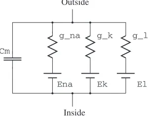
Due to the sodium-potassium pump operation the intracellular concentra-tion of K+ is much larger than the extracellular concentraconcentra-tion. The opposite holds for Na+. The Hodgkin-Huxley model treats the membrane permeability for each ion type as a non-linear conductance that is driven by the ion Nerst potential1 (Fig. 2.3). gN a, gK and gL are the membrane ion conductances
Cm
Ena Ek El
g_na g_k g_l
Inside Outside
Fig. 2.3. Hodgkin-Huxley model of the neural membrane
for Na+, K+ and leakages. EN a, EK and EL are the corresponding Nerst
potentials.Cm is the capacitance of the membrane.
When resting, the permeability (the “ease of penetration” through the membrane) of potassium ions is about 100 times larger than that of sodium ions. Related to Fig. 2.3,gK is 100 times larger thengN a. Thus the
intracel-lular resting potential is slightly larger thanEK. The actual resting cell
po-tential value varies for different cell types between−50 mV and−90 mV [17], measured with respect to the potential of the extracellular solution.
2.1.2 Action Potential
The membrane potential is subject to change, due to the activity of pre-synaptic neurons: neurotransmitters absorbed by the dendrites perturb slightly the membrane potential. The perturbations are accumulated, resulting in a gradual depolarization of the membrane. The ion channels open gradually due to the membrane depolarization, until it reaches a certain threshold, about 20 mV above the resting potential. Beyond this point, Na channels open rapidly, avalanche-like. Sodium ions enter the membrane, making the
1
8 2 Recording From Biological Neural Networks
inside of the cell positive. The intracellular potential is pulled towards the Nerst potential of Na+ ions, typically some 100 mV above the resting value. With the rise of the cell potential Na conductance declines back to zero. At the same time the potassium conductance rises and K+ ions flow out of the cell. At the potential peak the inward flow of Na+ is exceeded by the outward K+ flow and the potential swings towardsEK, even below its resting value. At this
point all the sodium channels are inactivated. The cell has gained some Na+ ions and has lost some K+ ions. The concentrations are restored by means of the sodium-potassium pump (energy consuming), during therefractory period
that lasts typically a couple of milliseconds (Fig. 2.4).
potential Resting Threshold
about 20mV
Vna V
g_na g_k
0mSec 1mSec 2mSec
Vk
Fig. 2.4.Action potential
A special note about action potentials must be made, from the neuron behavior perspective: Firing of an action potential indicates that the mem-brane depolarization has gone beyond a particular limit.The information in action potential is expressed in the bare fact of firing, and not in the shape of
the pulse. In digital communications this form of signalling is termed “pulse
position modulation”, or PPM.
2.1.3 Excitation Propagation
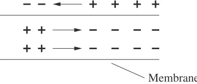
During an exhibition of action potential, there is a positive charge inside the cell (Na+ ions), while the extracellular volume adjacent to the soma is slightly negative. The excessive concentration of Na+ ions makes them flow out of the soma down the axon. Concurrently, outside the cell the Na+ ions flow towards the soma (due to the negative near the soma), Fig. 2.5. The current flow depolarizes an adjacent section of the membrane thus the excitation impulse travels along the axon. This form of propagation is called “uniform”.
2.1 The Neuron 9
Membrane
Fig. 2.5.Uniform excitation propagation
spaced points, thenodes of Ranvier Fig. 2.6. Since myelin is a good insulator,
Myelin
Ranvier node
Fig. 2.6.Saltatory excitation propagation
excitation can not occur except in the places where the myelin cover is thin-ner, nodes of Ranvier. The excitation propagates in “jumps” between adja-cent nodes and the impulse travels much faster: propagation speed in a myeli-nated nerve fiber is 80–120 m/S, while unmyelimyeli-nated nerve conduction speed is 0.5–2 m/S [12, 17].
Table 2.1 summarizes some of the physical properties of neurons.
Table 2.1.Typical values of neuron physical properties [18]
Soma diameter 5–20µm
Axon diameter 1–20µm
Membrane thickness 5 nm
Dendrite length up to 10µm
Axon length up to 1 m
Resting cell potential −70 mV
Action potential duration 1 mSec
10 2 Recording From Biological Neural Networks
2.2 Interfacing Neurons Electrically
In the biologic environment the currents are carried in the electrolytic medium by means of ion conduction. Electronic circuits, which are commonly used for transduction and processing of neural signals, all use electronic conduction.
Anelectrode (either recording or stimulating) provides transduction between
these two media. Numerous textbooks treat the electrode-electrolyte interface electrochemically [16] and electronically [17, 19, 20]. First reviews on electrode properties can be found in [21] and [22]. Additional reviews are available in [23] and in [24].
It must be noted that ionic mobility in biological medium is typically six orders of magnitude below the electron/hole mobility in metals or semicon-ductors [16], thus the time constants of the two media differ significantly: aqueous electrodes operate typically in 10 kHz bandwidth [19].
As we are going to present in detail, the electrode transduction takes place either by capacitive coupling or by charge transfer, in which electrons are transferred to and from the solution ions. The transfer occurs by two types of chemical reactions: oxidation (electrons are donated) andreduction (elec-trons are absorbed). When voltages across the interface are low, voltage-driven charge transfers across the junction are negligible and the capacitive effect prevails. This is the common case for recording, which is usually done with a high-impedance preamplifier and no DC currents across the electrode. This mode of operation typically involves small-signal measurements and electrodes are viewed as networks of linear elements (mostly capacitive).
When it comes to neurostimulation (involving non-negligible DC currents), a current flow is conducted through an electrode by means of carrier exchange. Large-signal model of an electrode must be considered, which involves elec-trochemical mechanisms of charge transduction [19].
2.2.1 Double Layer Capacitance
When an electrode is placed into an electrolyte, a space charge layer builds up at the interface due to various chemical reactions [16]. The build up con-tinues until a sufficiently strong electric field is formed to initiate a reverse reaction. At equilibrium forward and reverse reactions are equal and the net current across the junction is zero; the process resembles a PN semi-conductor junction.
The ion distribution in an electrolyte is modelled as a charge plane near the electrode (outer Helmholz plane, OHP), where the potential drops linearly, like in a common plate capacitor. The charge plane is followed by a cloud of mobile ions with approximately exponential potential drop (Fig. 2.7). The plate capacitance of the Helmholz layer can be calculated as:
CH =
ε0εrA
2.2 Interfacing Neurons Electrically 11
dOHP, the OHP distance from the electrode, is extremely small, typically less
than 10 ˚A. In [19], the worst-case capacitance of Helmholz layer is estimated at 0.11 pF/µm2.
A model for the capacitance of the mobile ions was suggested by Gouy and Chapman and is reviewed in [16]. It is voltage-dependent, as the ion distribution depends on the potential applied across the junction:
CD= ε0εr
LD
coshzV0 2Vt
whereV0 is the potential over the junction,Vtis the thermal voltage,zis the
ion charge, andLD is the Debye length:
LD=
ε0εrVt
2z2qn0
n0is the ion concentration in the solution (ions/liter).
Fig. 2.7.Metal-electrolyte interface potential. Adopted from [24]
The effective capacitance of the electrode-electrolyte interface is the su-perposition ofCD andCH:
For most biological solutions, when a zero bias is applied,CH andCD are of
the same order. A typical value of a net capacitance is about 0.05 pf/µm2[24].
2.2.2 Resistance at the Interface and Charge Transfer
To move charge into or out of the electrode a potential must be applied. Potential shift from the equilibrium valueV0 is called anoverpotential:
12 2 Recording From Biological Neural Networks
η=V −V0
There are four processes, each of them is associated with its overpotential. The total overpotential,η:
η=ηt+ηd+ηr+ηc
ηt is due to the charge transfer through the double layer, ηd is due to the
diffusion of ions in the electrolyte towards the electrode, ηr and ηc are due
to chemical reaction at the electrode and due to transfer of metal ions into electrolyte. The last two terms are usually insignificant in biological applica-tions [20].ηtdominates near the equilibrium. At higher currents,ηd becomes
significant due to the limited rate of ion supply from the bulk solution. At equilibrium, oxidation and reduction proceed at equal rates: J0 = JOX =−JRED. This equilibrium current density,J0, is calledexchange
cur-rent density. ηt can be related to the current density by the Butler-Volmer
equation:
J =J0(e(1−β)zηt/Vt−e−βzηt/Vt)
βis thesymmetry factor that reflects the differences in energy barriers of the two reactions. For small deviations from the equilibriumJ can be linearized (assumingβ of 0.5) as
J =J0zηt Vt
Thus the near-equilibrium charge transfer area conductance is
Gt=J0z/Vt
This value describes the charge transfer resistance in recording applications, where an electrode is coupled to a high-impedance preamplifier and the net current is zero. It is rather small: for 2×10⁻⁴, the largest value of J
0 among those brought in [19], it is only 80 pΩ−1/µm2. Thus an electrode with area of 1000µm2will have (at small bias)R
tof 12.5 MΩ.
In stimulation applications, where significant deviations from the equi-librium occur, Rt is significantly smaller. For instance, in a certain
experi-ment [25], a 100µA current was conducted through a 700µm2 electrode by applying only a 1V potential.
2.2.3 Diffusion Resistance Near DC
When an electrode conducts a steady state current, an ion concentration is increased near the electrode with respect to the bulk solution. The concen-tration is due to the diffusion of ions from the solution towards the electrode. The diffusion process causes an overpotential to be developed,ηd.
For any electrode, there is some limiting rate at which ions can be supplied from the bulk. LetJs be a corresponding limiting current density. Diffusion
2.2 Interfacing Neurons Electrically 13
J/Js= 1−e−|ηd|z/Vt
This equation is valid for near-DC conditions.
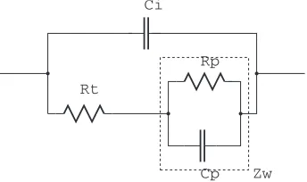
2.2.4 AC Diffusion Resistance
Imagine a sinusoidal potential applied to the electrode. It would force a si-nusoidally varying spatial concentration of ions. The variation will be largest at the interface and will decay deeper in the bulk. Damping of the variations will increase as the frequency increases. Thus the length to which the effect extends into the solution decreases with frequency and the concentration gra-dient at the interface increases with frequency, allowing more rapid supply of the ions to the interface. Therefore, effective impedance is smaller for larger frequencies.
The diffusion equations were solved by Warburg (the solution is reviewed in [16]). The solution is a frequency dependent parallel R-C impedance model, in series with a charge-transfer resistanceRt(Fig. 2.8).
Ci
Rt
Rp
Cp Zw
Fig. 2.8.Small-signal model of an electrode
BothRpandCpare frequency-dependent, and are given (for unit area) as:2:
Rp =
2σ ω1/2
Cp =
1 2σω1/2
σ= Vt
z2n0√2D
whereD is the diffusion coefficient of the ions. Warburg area impedance can be calculated as:
Zw= (Rp+jωCp)−1=
σ
ω1/2(1−j) 2
14 2 Recording From Biological Neural Networks
Besides thef−1/2frequency dependence this impedance has a constant phase of 45◦.
2.2.5 Electrode Noise
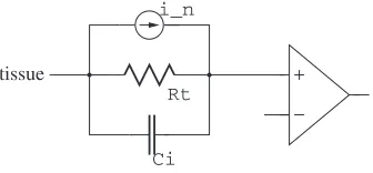
As we have seen above, the electrode impedance has an active (real) compo-nent along with a reactive (imaginary) compocompo-nent, therefore it must generate electronic noise. It has been shown in [22] and confirmed in [24] that the noise is thermal, and it is generated by the resistive part of the electrode impedance. To obtain an estimate of the electrode noise we shall consider two boundary cases for sample noise calculation: one where the electrode current is lim-ited by charge transduction through the interface (Rt) and another when the
current is diffusion limited (ZW).
We shall make all the calculations for a 1000µm2 electrode. Using the typical values we have seen above, the interfacial capacitance CI is about
50 pF and Rt (for charge transfer limited case) is 12.5 MΩ . If an amplifier
Ci
tissue
Rt i_n
Fig. 2.9.Rtlimited electrode
(Fig. 2.9) has an approximately infinite input impedance, then the noise power spectral density (PSD) at the amplifier input will be:
4kT Gt(
Taking the integral with respect tof:
vn2=
2kT πCI
arctan 2πf RtCI
For measurement bandwidth from DC to 10 kHz, since 2 π104R
tCI is much
larger than 1, we have:
vn2= 2kT
which is classic kT/C noise, independent ofRt. The RMS value is about 9µV .
For the diffusion-limited junction we shall take data presented in [17] (page 18, Table 1–4). It shows measurements ofCpof different electrodes in different
2.3 Neuronal Probes for Extracellular Recording 15
Cp=
k fα
by constantskandα. Among the presented cases, we select Pt/0.025N HCL, since its impedance is the closest match of Warburg model withαof−0.495 andkof 322µF/cm2. For 1000µm2electrodekis 3.22 nF. The corresponding value ofσis about 1/16·109sec1/2F−1. For simplicity of calculation we neglect CI with regard to Cp, although for frequencies around 10 kHzCp falls below
CI (32 pF vs. 50 pF). The equivalent circuit is much like Fig. 2.9, but we use
Rp andCpinstead ofRt andCI.
Integrating with respect tof:
vn2=
4kT σ
π ·
f
which is about 6µV RMS. This value is somewhat overestimated, since we have neglectedCI.
A practical electrode will probably be somewhere in between the two cases, i.e. its behavior will be affected by both the charge-transfer process and the diffusion process. Note, that in both cases the noise is inverse proportional to the square root of the electrode area. Thus a larger (and less selective) electrode will generate less noise.
2.3 Neuronal Probes for Extracellular Recording
Neuronal probes (or neuronal electrodes) are used to measure the electri-cal activity of neural networks. Above we have briefly discussed the electro-chemistry and electrical properties related to a generic metal electrode inter-facing a living tissue. This section describes different types of such electrodes
forextracellular recording, which means sensing the electrical current induced
in the extra-cellular solution by the electrical activity of nearby neurons. Re-views of different types of electrodes can be found in [26], in [27] and in [18]. It is important to note that a signal picked up during an extracellular measurement can not usually be related to a particular unit. Moreover, ex-tracellular electrode typically records activity from more than a single unit. The problem of identifying the active unit upon action potential discovery is usually referred to as “spike-sorting” (Chap. 6).
16 2 Recording From Biological Neural Networks
2.3.1 Penetrating Electrodes
Penetrating electrodes are usually thin needles, insulated along the entire length, with only the tip exposed. Traditionally, these are metal wires [21, 17]. The individual wires can be assembled into dense bundles for multi-site recording [28]. Such bundles are available commercially [29, 30].
Microfabrication techniques are used to produce multi-site electrode arrays on a silicon substrate (Fig. 2.10) [31, 32, 33], allowing for several potential advantages:
• Photolitography permits manufacturing precise recording site positions with uniform and repeatable characteristics.
• Thin film processing allows integrating multiple recording sites on a single silicon shaft, eliminating the need for work consuming assembly of discrete structures and reducing the overall device volume.
• Silicon substrate allows integrating electrode with on-chip circuitry, as was demonstrated in [33]. The recording and stimulating electronics was integrated with a multi-site probe of the “Michigan Probe” family.
The “Utah Microelectrode Array” [9] is another example of a micromachined multielectrode probe, consisting of a ten-by-ten array of 1mm silicon needles, glass isolated at the base.
(a) (b)
(c)
2.4 Recording from Cultured Neural Networks 17
2.3.2 Cuff Electrodes and Regenerating Sieve Electrodes
Cuff electrodes (reviewed in [26] and in [18]) are placed inside a tubular cuff warped around a nerve. Such electrodes may be used when inserting a pene-trating electrode is inappropriate, for example when the nerve is too deep.
Regenerating sieve electrode [34, 35, 36] is a thin “holed” plate. During the
implantation, the target nerve is cut, and the plate is placed inside the cut, in such way that nerve fibers (axons) regenerate through the holes in the array; the nerve “grows through” the plate. Sensing sites aligned near the holes sense only the fibers that pass through adjacent holes. Thus sieve electrodes (unlike cuff electrodes) are inherently selective to the different fibers in a nerve.
2.4 Recording from Cultured Neural Networks
Neuronal networks can be cultured out of the animal body on specialized devices, theMulti-Electrode Arrays (MEAs) [37, 38]. Recording from cultured networks has several advantages over in-vivo recording:
• Development of the network can be monitored under controlled and re-producible experimental conditions.
• Dense recording sites allow recording from a large number of neurons in small volumes, an impossible task to achieve by using microprobes and micromanipulators.
• Placement of neurons inside a cultured network can be forced, allowing development of patterned networks [39, 40], allowing studying the effects of network geometry on network behaviour.
Cultured networks are widely used in studies of neural network dynamics [41, 42]. They are also employed as biosensors for drug testing and environmental hazard detection [43, 44].
An MEA (first introduced in [37]), is a dish made of biocompatible ma-terial, such as glass, ceramic or silicon, with deposited sensing/stimulating sites, conducting wires and connection pads (Fig. 2.11). The entire device is insulated electrically, except for the electrode tips. The recording sites (usu-ally several tens for an MEA) are typic(usu-ally of 10–20µm diameter and 100– 200µm spacing. MEAs of various configurations in terms of electrode material, shapes and positioning have been fabricated. A review on MEA configurations and methods of fabrication is available in [46, 19].
2.4.1 MEAs on Silicon Substrate
18 2 Recording From Biological Neural Networks
Fig. 2.11. An MEA from Multichannel Medical Systems [45]. Multichannel Sys-tems, Germany. http://www.multichannelsystems.com
properties of neuron-silicon junctions are extensively treated in [51]. In sili-con multi-electrode chips (MECs) neurons are capacitively coupled to gates of FET transistors integrated on the substrate. Neural activity is measured as action potentials affect the current flow through transistor channels. It was shown also [52] that individual neurons can be stimulated, (i.e. action poten-tials excited) by underlying electronic circuitry capacitively coupled to neural somata through a thin oxide layer.
There are two types of recording circuits: The first approach [53] utilizes a neuron placed on top of a thin oxide layer of a MOS transistor as a gate. Electrical activity of the neuron affects the electrical field across the transistor oxide and modulates the current through the channel. Another approach [49, 47, 11] uses a floating-gate MOS, with the gate capacitively coupled to a neuron via thin oxide layer. Action potentials modulate the gate potential which in turn affects the drain-source current.
Both methods require a voltage bias ofVthto exist between the transistor gate and the chip substrate in order for transistor to conduct current. This bias increases the effects of electrochemical corrosion, due to increased currents through oxide cracks. Shappir et al. [48] overcome this drawback by using a depletion MOS, that allows recording with zero bias voltage at the expense of an additional processing step.
2.5 Typical Multi-Electrode Recording Setup
2.5 Typical Multi-Electrode Recording Setup 19
Fig. 2.12.Typical setup for multielectrode neuronal recording
headstage) and the stationary part (the host). Inside the neuronal interface,
signals acquired by the recording electrode arrangement are shaped (pream-plified, filtered, possibly digitized) by the recording front-end. Either a wired or wireless communication link transfers the signals to the stationary host. In case of communication over wires, some sort of mechanical strain relief solu-tion must be employed if the subject is to be let free. This is typically done by means of a “commutator”, a mechanical device connecting two cables that allows both sides to be rotated freely with respect to each other (Fig. 2.13). The host performs the necessary computation and datalogging steps on the incoming input signals and calculates the stimulation feedback. Stimulation instructions are sent back into the interface where they are applied to the stimulation electrodes by the stimulating front-end.
Numerous implementations of such interfaces are available [54, 29, 45, 55]. The headstages are typically assembled of discrete components on miniatur-ized printed circuit boards (Fig. 2.13). A construction of such a headstage was described in [56].
Various headstage components, especially the recording front-end circuits have been implemented on VLSI chips, providing a higher level of integra-tion. Various aspects of neuronal preamplifiers have been the subject of many studies: [58, 59, 60, 61, 62, 63, 64, 65, 66, 67, 68], including noise-power op-timization and DC input stabilization (reviewed in greater detail in Chaps. 4 and 5).
20 2 Recording From Biological Neural Networks
(a) (b)
(c)
Fig. 2.13. (a) 16-channel tethered headstage [54]. Plexon, Inc., US. http:// plexoninc.com (b) Wireless headstage [57]. (c) 16-channel commutator [54]. Plexon, Inc., US. http://plexoninc.com
calledmote) from [71] was used for wireless communication with a headstage in [72].
Power is yet another important aspect of neuronal interface operation. Successful attempts of remotely powering the front-end device by telemetry have been reported [70, 73]. Another report [69] describes an optically powered device with an integrated photo-voltaic cell.
A certain commonality among the existing devices is very relevant to our discussion: (almost) no computation is ever performed at the interface side. The front-end devices rely on the host “to be there” for any computation needed. In some exceptional cases, front-end circuit may measure some fea-tures of the recorded signal to assist the data processing on host. Two such cases (to the best of our knowledge) exist. In [62], the amplitude of a spike is measured. In [74] a threshold detection is applied, with the threshold level automatically calculated based on measurements of the input signal RMS.
2.6 Recorded Signal Information Content
2.6 Recorded Signal Information Content 21
or width) of the action potential waveforms. The times and the originating cells of the firing events therefore define the “informative content” in neuronal signals. After it is extracted from the recorded signal, higher level algorithms concerned with behavioral aspects of neuronal networks can be applied.
Extracting information out of the recorded signal can be divided into a pair of distinct tasks: detecting the firing events in the signal (so called
spike-detection) and recognizing their sources (spike-sorting). Since firing events
3
The Neuroprocessor
Wireless neuronal interfaces are in need in clinical practice, neuronal pros-thetics and neurophysiology research. In the former, they will eliminate the transcutaneous wires, improving the quality of life for the patients and re-ducing contamination risk. In the latter, they will allow recording from freely behaving animals that are not constrained by the connecting wires. Needless to say, such interfaces have to be powered by miniature-size power cells, yet they are to provide sufficient battery life. For human patients, it has to be days if the battery is rechargeable or years if the battery is to be replaced.
Conventional neuronal interfaces such as described in Chap. 2 serve as mere transducers of the signal between the host and the tissue. As such, they transmit all the recorded data and rely on a permanently available host to per-form the required computation/data logging. The communication bandwidth required for such operation can be easily calculated given the number of elec-trodes involved in the interface. There are indications that a good quality prediction of a limb movement may require recording from even thousands of cells [3, 76]. Experiments involving hundreds of cells were reported [3, 28]. The increase in the scale of neuronal interfaces is supported also by introducing microfabrication technologies into the development of neuronal probes, exam-ples are the 100-electrode Utah array [9] and the Michigan probe available with up to 64 channels [77].
Let us consider an interface of a hundred of electrodes, each sampled at 25 Ksps with eight bits of precision, the cumulative datarate is 20 Mbps, far too high for a system powered by a miniature-size battery. This observation was already reported in [74, 78]. It uncovers a fundamental limitation of the non-computational paradigm, showing it inadequate for interfacing large numbers of neurons wirelessly.
24 3 The Neuroprocessor
eliminating the need of permanent host connection completely. This is an im-portant advantage considering neuronal prosthetics, as a prosthetic device can hardly rely on the host to be constantly present.
3.1 Datarate Reduction in Neuronal Interfaces
Datarate explosion can be lowered to some extent, if we recall that infor-mation exchange inside neural networks is carried through neuronal firing. The times of neuronal firing events and their origins are the essential features in the recorded neuronal signals. Communicating the continuous signal from the recording electrode is a waste of bandwidth, knowing that neuronal firing events are relatively rare (up to tens of spikes per second) and do not last long (order of a millisecond); most of the time the electrodes record background noise. Preferrably, spike activity would be detected in the recorded signal and only signal portions containing such activity would be communicated. This approach for datarate relaxation was suggested in [74].
If an electrode is sampled at 25 KSps with eight bit precision, a hundred electrodes generate 20 Mbps. Assuming that a neuron fires twenty times a second on average and every electrode senses three to four neurons, the elec-trode would record close to a hundred spikes per second on average. Assuming also that a spike lasts 1–2 msec, the datarate can be reduced to 2–4 Mbps by detecting spikes in the recorded signal, and communicating only the active signal portions. Although about an order of magnitde bandwidth reduction can be achieved, the resulting datarates are still high.
Let us recall once again that what we seek in neuronal signals are the times of firing events and their sources. The times and sources of the firing events will be extracted from the recorded signal at the host by means of spike sorting (in a multi-unit experiment) or a mere spike detection (single-unit experiment). Communicating the analog waveforms of the signal, even clipped to the times of firing activity, is yet a waste of communication bandwidth. Detection and sorting would be preferrably done on the interface, limiting the communication to the mere indications of spikes and their sources. Using the figures as above, assuming that every spike results in 32-bit spike notification message, the cumulative datarate for a hundred of electrodes is only 320 Kbps, another order of magnitude datarate reduction. Such datarate can be communicated over low-power (tens of milliamps) wireless datalinks. Commercial products for such communication are already available: examples can be found at [71] (Zigbee standard [79]) or at [80] (MICS band).
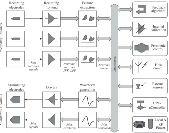
3.2 Neuroprocessor Overview
3.2 Neuroprocessor Overview 25
signals waveformsStim. commandsStim.
calibrationInternal
Fig. 3.1.Neuroprocessor conceptual architecture
Recording front-end brings the signals acquired by the recording electrodes into a form suitable for neuronal data extraction. This typically involves DC drifts removal, amplification and filtering (the front-end will be discussed in greater depth in Chaps. 4 and 5). Feature extraction may operate on digital or analog signals. Consequently, the front-end includes digitization.
The registered neuronal events may be used in different ways, depending on the particular applicaiton the Neurprocessor is used for: stimulative feedback calculation, prosthetic device control and/or indication to the host of the neuronal activity.
The stimulation path consists of waveform generation blocks driving stim-ulation electrodes. As the latter are typically large, their impedance tends to be significantly lower than that of the recording electrodes, potentially requiring special output drivers.
26 3 The Neuroprocessor
4
Integrated Front-End for Neuronal Recording
4.1 Background
A signal recorded by an extracellular microelectrode consists of several com-ponents in several frequency bands [81]. Neuronal firing activity occupies the 100–10.000 Hz frequency band. The amplitude of neuronal spikes picked up by an extracellular electrode is typically small, below 100µV . Another com-ponent of neuronal signal is the Local Field Potential (LFP). The LFP carries cumulative information regarding the activity of large ensembles of cells [75]. It was shown to carry useful information with regard to sensory response [82] and motion [83, 84]. LFP occupies the low-frequency band, below 200 Hz and exhibits much larger amplitudes, of up to 5 mV. Large (hundreds of millivolts) slow drifts of electrode potential are the third and the most “annoying” com-ponent of a recorded signal. These drifts are associated with electrochemical reactions at electrode-tissue interface.
The electrode noise (Chap. 2) together with the background noise define the noise floor. A typical setup may provide signals with several microvolt noise floor [24, 85].
4.1.1 Blocking the DC Drifts
28 4 Integrated Front-End for Neuronal Recording
Several approaches have been shown. Using off-chip capacitors in a feed-back path of an input amplifier is suggested in [58]. The corner frequency is set so that the LFP is blocked as well. The convenience of using large capacitors comes at the expense of an increased pin-count (an additional pin per chan-nel) and element count (an external capacitor per chanchan-nel). This latter issue makes this approach impractical for implanted or minituarized head-stages serving hundreds of channels.
In this context, we would like to point out that the signal can be high-pass filtered by subtracting the low-frequency component from the input. Some of the presented works [68, 58, 59] take this approach placing a low-pass filter (LPF) in a feedback path of an amplifier (Fig. 4.1).
Low−Pass filter Off−chip
(a) (b)
Fig. 4.1.(a) DC blocking with low-pass feedback. (b) Implementation in [58]
Fully integrated approaches were also demonstrated. One of the earli-est fully integrated neuronal preamplifiers was published in [59]. A diode-capacitor feedback path was utilized for low-frequency filtering. A diode typi-cally exhibits a very large small-signal impedance at near-zero current levels; this was used to achieve a large time constant. The drawback of the approach (as we see it) is that the input differential pair was placed outside the feedback loop. The DC drifts are blocked at the output of the first amplification stage. Large input offset may therefore drive the first stage far from the equilibrium point.
4.1 Background 29
electrode is usually not purely reactive, it has also a resistive part, usually very large, but not infinite. Thus the DC gain of this scheme is not strictly zero, although it can be made very small [64].
In [68] AC coupling was implemented with an integrated capacitor and a diode-connected MOS transistor as a shunting element. The DC gain of this arrangement is strictly zero. It was also suggested to place the coupling capacitor underneath the bonding pads to save die area. AC coupling with a subthreshold MOS device for shunting was also employed in [57].
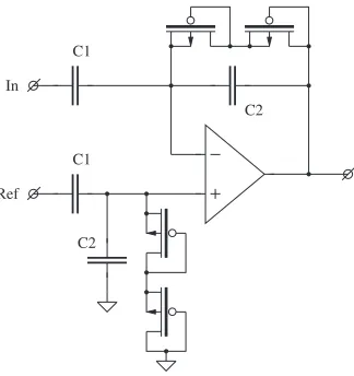
A different method was demonstrated in [63, 61, 86] (Fig. 4.2). The weak-inversion devices used in a feedback path provide for a very high small signal
In C1
C2
C1
C2 Ref
Fig. 4.2.Blocking DC with weak-inversion MOS devices
resistance at near-zero bias. When a higher voltage is applied across the device (in either direction) the current grows exponentially: either because of the opening of the MOS channel or because of the forward bias of the drain-substrate junction.1Thus the output voltage of this amplifier is forced within certain limits. In [62, 87] it was suggested to make the gate potential of the MOS devices adjustable. The corner frequency of the high-pass filter can thus be controlled.
[67] suggests a digital feedback for DC blocking: The output signal is to be digitized, processed and fed back to the amplifier negative input through a D/A converter. No implementation is published though, and the approach raises certain questions, regarding the implementation of a D/A converter with sub-millivolt accuracy and output noise at the microvolt level.
1
30 4 Integrated Front-End for Neuronal Recording
4.2
NPR01
: First Front-End Generation
The first recording front-end, fabricated also as technology and design plat-form validation step, included eight channels, each one consisting of a two-stage low noise single-ended preamplifier and a low pass filter. DC stabi-lization was achieved with input reset gates. Channel schematic is presented in Fig. 4.3. DC stabilization was achieved by periodically assertingφ1andφ2
Φ1 Φ2
Fig. 4.3.NPR01channel schematic
for short periods. Moreover, ifφ2is deasserted afterφ1is deasserted, then the output offset of the first stage is rejected at the second stage as well. A simple ring oscillator and the logic necessary for generationφ1,2 were also included on the chip.
The chip was fabricated in 0.35µm , double-poly, triple-metal mixed-signal process (AustriaMicroSystems), with 3.3V power supply. It was tested elec-trically and found functional. It was also tested as a preamplifier on an MEA-interfacing board (Fig. 4.4). It was observed during the experiments that reset gates introduce too much switching noise into the input signal. Single ended
(a) (b)
4.3 NPR02: Analog Front-End With Spike/LFP Separation 31
architecture of the amplifiers provided poor PSRR, allowing large supply in-terference. Both the supply interference and the switching noise completely obscured the neural activity. Two conclusions were made: The reset gate ap-proach for stabilization of the input DC level was proved impractical and abandoned; differential input stages were employed in the following genera-tions of sensing chips.
4.3
NPR02
: Analog Front-End With Spike/LFP
Separation
The second version of the front-end chip [88],NPR02 , included twelve
fully-differential recording channels each with a complete neuronal signal shaping chain. DC blocking was achieved with a first order high-pass filter at chan-nel inputs employing integrated resistors and off-chip capacitors.NPR02 also
introduces band-splitting of a neuronal signal into spike data and LFP. The chip was fabricated in 0.35µm double-poly, quad metal mixed signal process by AustriaMicroSystems.NPR02operates on a dual-rail supply of +/−1.65 V.
4.3.1 Splitting Spike and LFP
Cleared of the near-DC drifts, the neuronal signal has two components left: the spiking activity (occupying frequencies of 0.2–10 kHz) and the local field potential (below 100–200 Hz). Preferably, both are made available at the out-put. However, the combined signal is hardly usable, since the algorithms that operate on spike data require clearing the LFP and vice versa. Spikes and LFP must therefore be separated and provided on two separate outputs. The separation can be done in the digital domain, by digitizing the combined sig-nal and applying digital filtering afterwards. It can also be done in the asig-nalog domain, potentially saving some power.
Since spikes are rare events, if one can detect (or even suspect) their pres-ence in the signal by analog computation, then the digitizer can be activated only on the portions of the signal when a spike is suspected. Threshold de-tection, for example, is easily done in analog domain. Making digital compu-tations, on the other hand, requires the digitizer and the splitting filters to operate continuously. Making separate analog outputs with spike and LFP information can therefore potentially lead to power saving on the digitizer and subsequent digital filters.
32 4 Integrated Front-End for Neuronal Recording
split the signal, the maximum dynamic range is at the spike part, which is now defined by the noise floor and the spike amplitude and is ten times lower. Thus the dynamic range of the parts of the analog chain following band split-ting needs be only 100; and seven bits of resolution at the digitizer. The input preamplifier must provide a full dynamic range in both cases.
4.3.2 NPR02 Architecture
The architecture of a singleNPR02channel is shown in Fig. 4.5.
input DC block x100 Band Split
VGA
x10 VGA LPF
LFP
Spike
Diff.
Fig. 4.5.NPR02channel architecture
The signal is cleared of the DC component, amplified a hundred times and split into the spike and LFP parts. The spike part is then amplified by ten and amplified again by a variable gain amplifier. Spike band is limited by a second order Bessel filter with variable cutoff frequency. The LFP part is amplified by a variable-gain amplifier (VGA). Both spike and LFP outputs are buffered to chip pads.
Figure 4.6 shows the block diagram of anNPR02channel. The input
high-pass filter makes use of external capacitors. 8 MΩresistors (high resistive poly) were placed on chip. To make a cutoff at about 1 Hz, 22 nF external capacitors can be used, available in miniature SMD packages. The band splitter was realized as a first order RC filter, with 5 MΩresistor and 160 pF (gate oxide) capacitor.
Assuming the output LPF has a steep rolloff above some frequencyfb, the
noise introduced by the splitter into the spike band is:
4kT ·R·fb
which is about 30µV forfb of 10 kHz. The noise floor of the channel is aimed
at a level of 2–3µV . To suppress the splitter noise reliably, the preamp must provide gain of well above 20; the preamp gain was set to 100. Both VGAs provide digitally selectable gains of 2.5/5/7.5/10. The maximal total gain of the spike chain is therefore 10,000, and that of the LFP chain is 1,000.
4.3 NPR02: Analog Front-End With Spike/LFP Separation 33
DAC
Reg
DAC
Reg
LPF
freq. splitter
Global control signals LFP gain Spike gain LPF frequency NULL
x10
VGA
VGA
Internal Chip Bus
LFP
Chip pad inputDiff.
SPK
x100
buf
Fig. 4.6.NPR02block diagram
programmable resistor
buf out
in
ctl<2:0>
Fig. 4.7.Spike output LPF
DC offsets of both spike and LFP channels have to be compensated: The LFP channel amplifies the input preamp offset (hundreds ofµV , typically) by up to 60 dB; unless compensated, it would limit the dynamic range severely or even saturate the VGA. The spike chain output offset is determined by the offset of the×10 stage amplified by 40 dB, as the DC part of the preamp output signal is blocked by the band splitter. Smaller than LFP, spike offset is yet significant: the×10 stage has larger input offset compared to the preamp, since the latter uses very large input devices due to the noise requirements.
34 4 Integrated Front-End for Neuronal Recording
ladders, having 400 mV output swing. DAC values are stored in registers that can be individually accessed through a common bus with five address/data bits and three control bits.
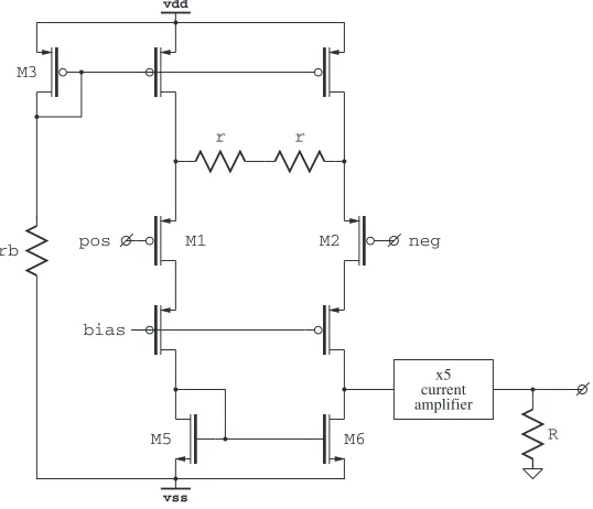
4.3.3 Input Preamplifier
The circuit of the input preamplifier is shown in Fig. 4.8. A degenerated dif-ferential cascoded transconductor stage followed by a current amplifier loaded
M6
vdd
vss
current amplifier
x5 pos
rb
r r
neg
M1 M2
M3
bias
R M5
Fig. 4.8.NPR02input preamplifier
with a resistor to convert the output current to voltage. The gain of the input stage is given by:
A= 2R
r+rm
= 2R/r
1 +rm/r
where rm is the transresistance of M1,2. While r can be matched to R by using the same resistor types and employing appropriate layout techniques, there is no straightforward way of matchingr to rm. The sensitivity to rm
can be reduced by reducing the ratiorm/r, but there is a limit on how high
rcan be due to the noise requirements (some 10 kΩ) and reducingrmmeans
more power.
Instead, we match rto rmby appropriately controlling the bias currents
throughM1,2.M1,2 are operated in the subthreshold region (the smallestrm
4.3 NPR02: Analog Front-End With Spike/LFP Separation 35
thus we can write the gain as:
A= 2R
r+rbVddηV−thVgs3
We match rb to r and keep Vgs3 much lower than Vdd. Since the ratio of
Vth and Vdd is small, the above expression becomes weakly dependent on
process parameter η and on Vgs3. The chip is expected to work in constant temperatures (subject body), thus the dependence on V th is not worrying. One sigma chip-to-chip channel gain variation of less than 2% was actually measured.
The procedure for sizing the preamp and choosing transistor current is de-scribed in Appendix A. Without going into too much detail here, the evident drawback of this circuit is the degeneration of the input differential pair. On one hand it is desirable to control the gain; on the other hand it reduces the ef-fective input transconductance, degrading the power-noise performance (more noise for a given power). From this perspective, feedback circuits such as [63] and alike perform better: the gain is set by the feedback and no degeneration is needed.
However, there is also an advantage, a low input capacitance. Feedback circuits use a large input capacitor (10 pF typically). Input capacitance of the preamp is lower: gate capacitance of the input transistor is some 5 pF and it is reduced by degeneration. The effective input capacitance for the circuit shown is about 700 fF.
Because of the low input capacitance, the preamplifier designed forNPR02
was also used in a chip for in-vitro recording (Chap. 7). The recording sites in such a chip typically provide much lower interface capacitance (i.e. coupling capacitance between the tissue and the preamplifier), thus low capacitance at preamplifier input is essential.
4.3.4 NPR02 Measurements
Measurement setup and test board block diagram are presented in Fig. 4.9. The layout and the assembled board are shown in Fig. 4.10. The test-board includes a matrix of digitally controlled switches that connect inputs
ofNPR02with a voltage divider driven by a waveform generator. The outputs
36 4 Integrated Front-End for Neuronal Recording
Voltage Divider
Switch Matrix
Waveform Generator
Switch Matrix
Output Channel #2
Output Channel #1
Scope NPR02
CPLD
PC
GPIB bus
NPR02 test board
Fig. 4.9. NPR02measurement setup
The switches andNPR02are controlled by an on-board programmable logic
device, that communicates with the computer host via a parallel port. The host also controls the waveform generator and the scope by means of a GPIB bus. This allows for developing fully automatic measurement procedures with MATLAB “Instrument Control” toolbox forNPR02evaluation.
(a) (b)
Fig. 4.10.(a)NPR02micrograph. (b)NPR02test board
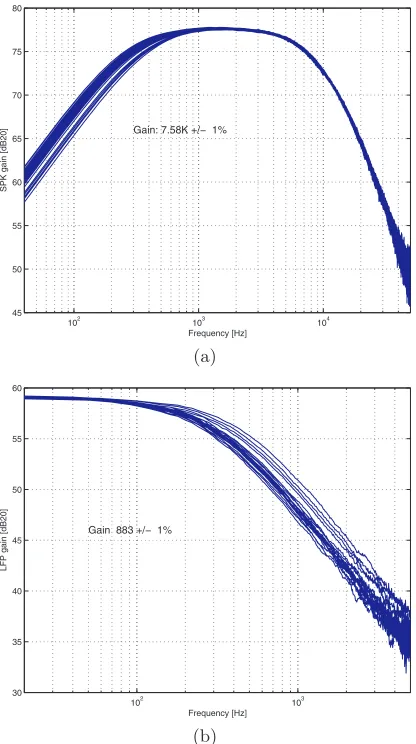
4.3 NPR02: Analog Front-End With Spike/LFP Separation 37
102
103
104
45 50 55 60 65 70 75 80
SPK gain [dB20]
Frequency [Hz] Gain: 7.58K +/− 1%
(a)
102
103
30 35 40 45 50 55 60
LFP gain [dB20]
Frequency [Hz] Gain 883 +/− 1%
(b)
Fig. 4.11.NPR02frequency response: (a) spike. (b) LFP
The conclusion is that the statistical models are rather pessimistic. If the cir-cuit is to be redesigned, we can allow much smaller degeneration and reduce power consumption. If we repeat the calculations for preamp sizing described in Appendix A using three times smallerr/rm, the current consumption goes
down to 40% of the present value.
38 4 Integrated Front-End for Neuronal Recording
to bring the MOS capacitance to its largest. This was done with a special bias block, which has failed.
Figure 4.12 shows the input-referred noise measured with NPR02 , along
with the simulated curve. The measurements agree with expectations. Total input referred noise (spike channel) is 3µV .
102 103 104
1016 1015
F [Hz]
PSD [V
2/Hz]
(a)
102 103 104
1018 1017 1016 1015
F [Hz]
PSD [V
2/Hz]
(b)
5
NPR03
: Mixed-Signal Integrated Front-End
for Neuronal Recording
5.1 Overview
NPR03 [90] is a fully integrated mixed-signal twelve-channel front-end. DC
regulation is obtained with an input high-pass filter built of weak-inversion MOS devices and integrated capacitors. The corner frequency of this filter is digitally programmable with gate bias voltage setting by special DACs.
NPR03 has differential inputs, spike/LFP band separation and digital offset
calibration. Spike/LFP gains and output LPF cutoff frequencies are digitally programmable for each channel.
A 10-bit analog-to-digital converter (ADC) is integrated in every channel. A special “inverted dual-ladder” resistor DAC [91] was designed to be used in the ADCs. The channels communicate with the central controller over an in-ternal synchronous bus. The controller takes care of channel readout, inin-ternal bus mastering and host communications over a five-wire bit serial synchronous line (McBSP [92]). All the channel parameters (offsets, gains, corner frequen-cies) and controller registers are accessible by the host through the McBSP interface. The same interface is also used for streaming the recorded data to the host. NPR03 can also be instructed to apply threshold detection on the
recorded channels and stream only active portions of the recorded signals (signal clipping).
A special system incorporating an evaluation board and an embedded computer communication board was designed to interface theNPR03with the
host computer via Ethernet line. Host-side software with a Graphical User Interface was developed forNPR03 control and data display.
The improvements introduced in NPR03 compared to NPR02 are
summa-rized below.
40 5 NPR03: Mixed-Signal Integrated Front-End for Neuronal Recording
• All the parameters of the recording channels are stored in dedicated reg-isters inside the channel. VGA gains and filter frequencies can be set for every channel individually (in contrast withNPR02).
• Ten bit channel-level ADCs allow for digitization of recorded signals at 40 KSps.
• The channels are accessed through an internal synchronous bus, both for register setting and for readout of the recorded signals.
• Chip operation is timed by an integrated controller. The controller is re-sponsible for the internal bus management, register access, data readout, multiplexing and host communications.
• Host communication is carried out over a five-wire, synchronous, serial bus.
• The controller is capable of “signal clipping”: it can apply threshold detec-tion to the incoming signal and communicate a certain number of samples from a channel after a threshold crossing event has been detected on this channel.
Figure 5.1 shows the layout ofNPR03.
Fig. 5.1.NPR03layout
5.2
NPR03
Architecture
The block diagram ofNPR03is shown in Fig. 5.2.
5.2 NPR03Architecture 41
Fig. 5.2.NPR03block diagram
transmits the active signal segments to the host. All twelve channels or an arbitrary subset thereof can be enabled for data streaming.
A threshold crossing event is triggered for a certain channel when the output of this channel falls below the low threshold or rises above the high threshold. A certain number of samples from that channel will be communi-cated to the host following the threshold crossing event. The threshold values and the number of samples to transmit after the threshold event are pro-grammable. The entire data stream, without clipping, can be obtained from the chip by setting both thresholds identical.
5.2.1 Chip Communications
The chip communicates over a McBSP bus [93]. This is a five-wire, full-duplex, bit-serial synchronous bus; a synchronization clock signal is constantly sup-plied by the host. Communication is carried out in frames; the host sends 24-bit frames (we refer to this direction asdownwards) and the chip replies with 16-bit frames (theupwardsdirection). The lengths of downward and up-ward frames were conveniently chosen to match the lengths of a single host instruction packet and a single reply packet respectively.NPR03downward and
upward frame formats are described in Appendix B.
42 5 NPR03: Mixed-Signal Integrated Front-End for Neuronal Recording
5.2.2 Instruction Set and Register Access
The chip operation is controlled through instructions sent via the McBSP bus. Four instructions are available:
• STORE reg val: Store value in a register.
• FETCH reg: Fetch register contents.
• RUN: Start streaming data.
• STOP: Stop streaming data.
There are two kinds of parameters that control the chip, those affect-ing controller operation and those affectaffect-ing the channels. The former include clock divider settings, threshold values, number of samples to communicate upon threshold detection and channel enabling bit mask; the registers for their storage reside in the controller and are accessed directly. The latter in-clude offset calibration data, channel gains and filter frequencies; the registers are distributed over the channels and are accessed through the internal bus.
NPR03registers and their functionality are described in Sect. B.2.
The internal bus has eight data lines, two control lines and a clock. A reg-ister connected to the bus is identified by a distinct eight-bit address. Every bus access is carried out in two steps; during the address step (ADDRis high)
the address is driven onDTA<7:0>. The register matching this address is
se-lected. During the data step (ADDRis low) the contents of the selected register
are driven on the bus by the channel (WRis low) or the register is updated
with the value on the bus (WRis high). The bus can be accessed in three
possi-ble scenarios,SELECT-READ,SELECT-WRITEandSELECT-READ-MODIFY-WRITE.
Figure 5.3 shows the bus signals during the last access scenario.
5. register updated
CLK
2. channel selected
WR
ADDR
1. host asserts ADDR
drives address on bus 3. register value
driven on bus
4. host asserts WR drives data on bus
DTA<7:0>
Fig. 5.3.SELECT-READ-MODIFY-WRITEbus access
5.3 Host Interface 43
conversion at the channel ADC. Reading a single ADC sample out of a channel takes therefore five clock cycles. 16 channels sampled at 40 Ksps need bus clock rate of at least 3.2 MHz. Since the bus clock is derived form the McBSP clock by integer division, the most suitable division factor is 3, setting the bus clock to about 4.16 MHz.
5.3 Host Interface
A special interface provides for communication between a personal computer and the neuronal recording front-end. The basis of the interface is an Al-tera Nios II development kit board incorporating an AlAl-tera Cyclone II FPGA device, RAM and flash memory, and an integrated Ethernet physical inter-face/MAC (Fig. 5.4).
C++ low level stream handling Windows XP
Java GUI & waveform display uC/OS RTOS
McBSP peripheral device driver Real−time communication software
DMA0
To NPR03 PHY / MAC
Altera Cyclone II FPGA device
Custom
Embedded Altera Avalon bus
Fig. 5.4.NPR03host interface board
The FPGA incorporates an Altera Nios II embedded processor core, bus logic and custom-developed peripheral for McBSP communications with the neuronal recording front-end. The embedded processor executes the µC/OS real-time operating system (RTOS) and custom-developed real-time software for handling the neuronal data stream. The software reads the serial McBSP data, packetizes it and transmits the packets over Ethernet to a host computer using UDP/IP protocol. It also handles the incoming instructions from the host and communicates them to the chip.
44 5 NPR03: Mixed-Signal Integrated Front-End for Neuronal Recording
(a) (b)
Fig. 5.5.(a)NPR03evaluation board and host interface. (b) screenshot of the host-side software
5.4
NPR03
Channel
The block diagram of theNPR03recording channel is shown in Fig. 5.6. Most of
the analog circuitry was left unchanged fromNPR02. The input preamplifier,
designed anew, is an exception and is discussed below.
5.5 Analog-to-Digital Converter
A 10-bit successive approximation ADC was added at every channel. It was intended to operate at 40 kSps sampling rate and provide input range close to the supply rails. The ADC employs a dual resistive ladder 10-bit DAC, comparator, digital controller and sample-and-hold.
Miller sample-and-hold was utilized (Fig. 5.7). The convenience of this scheme is that the opamp inputs are always kept close to ground potential, thus it does not require a rail-to-rail opamp input even when the whole circuit does operate rail-to-rail. A simple opamp with cascoded output stage was used in the SAH.
A rail-to-rail comparator was designed for the ADC (Fig. 5.8). Rail-to-rail operation was achieved with two complimentary input differential pairs; the pairs are followed by a summing stage and a latch.
A novel, dual resistive ladder DAC [91] was developed for inNPR03.1 In a
single resistive ladder DAC, the current flow is inversely proportional to the ladder resistance, while the output impedance (and thus, the settling time) is directly proportional to the ladder resistance. Therefore, current consumption multiplied by the settling time is a constant. Ten-bit DAC is hard to implement with a single ladder, due to the large number of taps to break out. Above eight
1
![Fig. 2.7. Metal-electrolyte interface potential. Adopted from [24]](https://thumb-ap.123doks.com/thumbv2/123dok/4034464.1977884/18.441.121.319.257.413/fig-metal-electrolyte-interface-potential-adopted-from.webp)
![Fig. 2.10. Microfabricated probes. (a) [32]. (b) [31]. (c) [9]](https://thumb-ap.123doks.com/thumbv2/123dok/4034464.1977884/23.441.116.338.320.554/fig-microfabricated-probes.webp)