Power-efficient Body Bias Control
for Ultra Low-power VLSI Systems
Hayate Okuhara
A thesis for the degree of Ph.D. in Engineering
Under the supervision of Prof. Hideharu Amano
Graduate School of Science and TechnologyAbstract
The power consumption of CMOS VLSI is still one of the main concerns for IoT demands. This is because available energy sources might be limited in some cases when the IoT nodes operate with quite tiny batteries (e.g. wearable computing, sensor systems, and health monitoring systems). On the other hand, recent transistors suffer from detrimental effects such as leakage current and process variations. Both of them increase the entire system power and degrade the battery lifetime; thus, they should be efficiently suppressed.
Body bias control is one of the most efficient means to address these issues. It can widely provide an efficient tradeoff between leakage power and gate delay by adjusting the transistor threshold voltages even after chip fabrication. In addition, the body bias effect is further endorsed with the unique transistor structure of Fully Depleted Silicon on Insulators (FD-SOIs). Moreover, this technology provides some good features such as low fabrication cost, high performance, and low-power consumption. Thus, leveraging FD-SOI and body bias control can be an efficient solution for a low power VLSI design.
Despite the advantages offered by body biasing, a crucial design challenge is intro-duced, namely, how to find the optimal voltage settings (i.e. power supply and body bias voltages). Improper voltage selection might cause excessive current consumption or timing violations. In this thesis, a power optimization methodology obtaining proper voltage set-tings is proposed and evaluated. Compared to the other conventional studies, the proposed method can improve the power/performance control granularity of body biasing. Since the proposed approach assumes conventional voltage sources, it allows utilizing given voltage regulators more efficiently compared to the conventional methods.
In addition, the overhead incurred by the body bias control has to be taken into account for low power applications. Conventionally, digital-analog converters are often adopted for body biasing because of their fine voltage controllability. However, such analog circuits require a high-power supply voltage and an additional power source, resulting in a con-siderable power overhead and an increased system cost. When a system needs to operate at a limited power budget such as an order of milliwatt, these factors cannot be ignored. Therefore, in order to achieve a lower power overhead, an on-chip digitally assisted auto-matic body bias tuning scheme (DABT) is proposed in this thesis. Thanks to the proposed architecture, it can operate even at 0.35V of power supply voltage. A power source for digital circuits can be shared with the proposed body bias controller even when its voltage
ii Abstract
is set to a near-threshold region. As a result, the proposed architecture does not require any additional power sources.
These proposed methods are validated with real chips fabricated with the SOTB-65nm technology. The evaluation results show that, when compared to conventional methods, the proposed power optimization can achieve 9.62% of average power reduction reaching up to 22.77% in the case of the V850 microcontroller.
Also, the proposed DABT mechanism can operate with a power overhead which does not exceed a fewµW. To the best of the author’s knowledge, this is the lowest power over-head among the already fabricated controllers to date.
Acknowledgement
During my doctor studies, I have been supported by a lot of people Thanks to their kindness, I have improved the quality of my research and could finish writing this thesis.
First of all, I would like my deepest gratitude and thanks to my supervisor professor Hideharu Amano also known as “Hunga-san”. Hunga-san provided with me an excellent environment where I could comfortably work. He has always welcomed any constructive discussions, which have definitely reinforced the quality of my research. I have learned a lot of things during my time in theHunga-laboratory.
I would like to also thank professor Kimiyoshi Usami, professor Nobuyuki Yamasaki, and professor Tadahiro Kuroda (These names are listed in alphabetical order). They kindly accepted to review this thesis and provided many constructive comments.
The study of Digitally Assisted Automatic Body Bias Tuning Scheme in Chapter 5 is based on the IP of VBBGEN provided by Ishibashi laboratory in The University of Electro-Communications. So I would like to also thank professor Koichiro Ishibashi, Mr. Tomoaki Koide, and Mr. Hiroki Nagatomi for supplying the IP.
I am greatly indebted to Dr. Akram Ben Ahmed, Dr. Nguyen Anh Vu Doan, and Dr. Johannes Maximilian Kühn for their continuous support and their valuable advice to improve my research and English skills. In addition to the above persons, I am grateful for all of theWASMII group members for offering me daily inspirations and so much fun for me.
Last but not least, special thanks go to my beloved family who helped me succeed in my studies.
Hayate Okuhara Yokohama, Japan August 2018
Contents
Abstract i
Acknowledgement iii
1 Introduction 1
1.1 Low power VLSI system demands . . . 1
1.2 Technology trends of CMOS VLSI . . . 1
1.3 Obstacles for IoT demands . . . 3
1.4 Design challenges . . . 4
1.5 Overview of the proposed approaches . . . 5
1.5.1 Power optimization . . . 5
1.5.2 Body bias controller . . . 6
1.6 Outline of this thesis . . . 7
2 Preliminaries and Background 9 2.1 System on Chip . . . 9
2.2 Power consumption on CMOS VLSI . . . 13
2.2.1 Dynamic power . . . 13
2.2.2 Static power . . . 14
2.2.3 Power and delay trade-off . . . 16
2.3 Body bias control . . . 18
2.4 Fully Depleted Silicon on Insulator . . . 19
2.5 Process variation . . . 21
2.6 On chip voltage generators . . . 23
2.6.1 DC-DC converter for power supply . . . 23
2.6.2 Voltage generators for BBC . . . 25
2.7 Optimal voltage selection . . . 27
2.7.1 Energy optimization . . . 27
2.7.2 Power optimization . . . 28
2.8 Summary . . . 29 v
vi Abstract
3 Motivation 31
3.1 Restriction on conventional optimization methods . . . 31
3.2 Overhead of Body Bias Controller . . . 39
4 Power Optimization Enabling Asymmetric Body Bias Control 43 4.1 Adopted Power and Delay Models . . . 43
4.1.1 Power consumption . . . 43
4.1.2 Operational frequency . . . 45
4.1.3 Accuracy of the proposed model . . . 46
4.2 Power optimization and result . . . 50
4.2.1 Assumptions and considerations . . . 50
4.2.2 Initial optimization . . . 50
4.2.3 Error adjustment . . . 51
4.2.4 Optimization results . . . 52
4.2.5 Body bias asymmetricity . . . 56
4.2.6 Hardware implementation and overhead analysis . . . 59
4.2.7 Threshold voltage variations . . . 60
4.3 Noise margin . . . 62
4.4 Summary . . . 65
5 Digitally Assisted Automatic Body Bias Tuning Scheme 67 5.1 Digitally Assisted Automatic Body Bias control scheme (DABT) . . . 67
5.1.1 DABT concept overview . . . 67
5.1.2 Performance emulator and Charge-pump . . . 69
5.1.3 Discharge circuit and Phase-frequency detector . . . 70
5.1.4 Wake-up detector . . . 72
5.2 Evaluation . . . 74
5.2.1 Chip implementation & Measurement setup . . . 74
5.2.2 Chip measurement results . . . 77
5.2.3 DABT impact on a processor system . . . 89
5.3 Conclusion of this chapter . . . 93
6 Conclusion and Future Work 95 6.1 Conclusion . . . 95
6.2 Future Work . . . 96
Bibliography 97
List of Figures
1.1 The number of IoT nodes . . . 2
1.2 Minimum feature size scaling trend for Intel logic technologies [10] . . . . 3
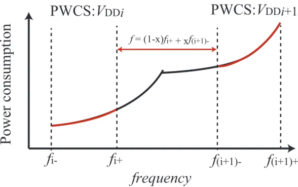
1.3 Conceptual waveform of the BBC . . . 5
1.4 Thesis structure . . . 8
2.1 Simplified block diagram ofBlack ghostarchitecture . . . 10
2.2 Simplified block diagram of the self-powered IoT edge from Intel . . . 10
2.3 Simplified block diagram of the RISC-V SoC . . . 11
2.4 Simplified block diagram of the BrainSoC . . . 12
2.5 Simplified block diagram of the near threshold SoC in [37] . . . 12
2.6 Power consumption on CMOS VLSI (a) Dynamic current (b) Leakage current 14 2.7 Voltage control technique: (a) Power supply control (b) Body bias control . 15 2.8 Break down of the power consumption . . . 16
2.9 Power gating: (a) header switch (b) footer switch . . . 17
2.10 Trade-off between the power consumption and gate delay (f = 200M Hz) . 18 2.11 Body bias effect simulation. . . 20
2.12 Cross-sectional view of MOSFET: (a) FD-SOI (b) Bulk. . . 21
2.13 Process variation effects on a FD-SOI. The SOTB 65-nm technology is used. (nMOS/pMOS=FF,TT,SS): (a)Leakage power (b)Gate delay . . . 24
2.14 Various types of DCDC converters: (a) Buck converter (b) LDO (c) Switched capacitor. . . 25
2.15 Simplified block diagram of VTCMOS. . . 26
2.16 Simplified diagram of a DAC-based body bias generator. . . 27
2.17 Body bias tuning system using a DAC-based controller. . . 27
2.18 Power optimization considering the restrictions of an actual power supply source. . . 29
3.1 Relationship between the gate delay and static power under the various body bias voltages (VDD = 0.6V):(a) INV (b)2NAND (c)2NOR . . . 33
3.2 Simulated body bias dependency to the threshold voltage (+:FBB -:RBB) . 34 vii
viii Abstract
3.3 Concept of the body bias control at the condition where the number of volt-age patternkis equal to 2. We have {V BN0, V BN1} for nMOS body bias
and {V BP0, V BP1} for pMOS: (a) Symmetric (b) Asymmetric. . . 35
3.4 Photos of the tested chips: (a) V850-Estar (b) MuCCRA4-BB. . . 36
3.5 Leakage current characteristics vsfmax: (a) V850-Estar (b) MuCCRA4-BB. 37 3.6 Extracted optimal voltage conditions with asymmetric BBC: (a) V850-Estar (b) MuCCRA4-BB. . . 38
4.1 Leakage current of FD-SOI (a) characteristics ofVDD(b) characteristics of V BN . . . 44
4.2 VDDfrequency characteristics at zero bias state. . . 45
4.3 Error of the leakage current model (a) power supply dependency (b) body bias dependency :V850-Estar (c) body bias dependency: MuCCRA4-BB. . 47
4.4 Error of thefmaxmodel (a) power supply dependency (b) body bias depen-dency :V850-Estar (c) body bias dependepen-dency: MuCCRA4-BB. . . 49
4.5 Data structure obtained by the model. The voltage combinations (i.e.,VDD, V BP, V BN), are denoted by Combv(v = 1, ..., k×k×i). The power minimum point in each frequency group is represented byPmin. The true optimal power consumption at fn of operational frequency is defined as OptP n(fn). . . 51
4.6 Error compensation step in the proposed optimization. . . 53
4.7 System total power consumption comparison results:(a) V850 (b) MuCCRA4-BB. . . 55
4.8 Effect ofVDDvoltage scaling. . . 56
4.9 Voltage asymmetricity of the optimization results :(a) V850 (b) MuCCRA4. 58 4.10 On-chip implementation of the Error adjustment phase. The highlighted parts are the additional components to the conventional body bias control scheme. . . 59
4.11 Power optimization results under the threshold variations . . . 61
4.12 Simulated noise margin: (a)N MH (b)N ML. . . 63
4.13 Definition of the butterfly curve and static noise margin . . . 64
4.14 Simulation results of the static noise margin: VDD=0.4V . . . 64
5.1 Simplified block diagram of DABT . . . 68
5.2 Performance emulator and Charge pump architecture . . . 70
5.3 Simulated waveform of VBBGEN . . . 71
5.4 Discharge circuit and Phase and frequency detector architecture . . . 71
5.5 Timing diagram of the discharge circuit and phase-frequency detector . . . 72
5.6 Wake-up detector . . . 73
5.7 Timing diagram of the wakeup detector . . . 73
5.9 Layout of DABT . . . 75 5.10 Testing board for the real chip measurements . . . 76 5.11 Oscilloscope waveforms snapshots depicting the behavior of the proposed
system . . . 77 5.12 VBBGEN output voltage without body bias control . . . 78 5.13 Measured power consumption for the standby mode . . . 79 5.14 Measured waveform for the voltage transition from the standby mode to
active mode: (a) 2.56mm2of load (b) 0.1mm2 . . . 81 5.15 Measured characteristics of the active mode at 0.5V of VDD: (a) Output
voltage (b) Power consumption . . . 82 5.16 Measured characteristics of the active mode at 0.35V of VDD: (a) Output
voltage (b) Power consumption . . . 83 5.17 The power breakdown of DABT at room temperature: (a)VDD = 0.5V
(b)VDD= 0.35V . . . 84
5.18 Available input frequency range of DABT . . . 86 5.19 Measured frequency deviation of DABT . . . 87 5.20 Used layout for the simulations: (a) Entire system (b) Bias controller . . . . 89 5.21 Difference of the delay between the performance emulator and MIPS. . . . 90 5.22 Leakage reduction for MIPS processor. . . 91 6.1 Appropriate situations to apply the proposed methods . . . 96
List of Tables
1.1 Leakage current of each process feature size [13] . . . 3
2.1 Summary of body bias control . . . 19
3.1 Implementation conditions of the tested chips. . . 34
4.1 Coefficients of the model. . . 48
4.2 Summary of the error of the proposed model. . . 48
4.3 Used Voltage sets for the proposed optimization evaluation. . . 54
5.1 Area breakdown of the implemented components in DABT . . . 74
5.2 Summary and comparison with the other fabricated body bias control sys-tems: ∗The summarized slew rate values are for the body bias transition from the standby mode to the active mode. †The power consumption is obtained at 0.35V ofVDD and 0.1MHz of f. ‡The power consumption is obtained at 0.5V ofVDDand 14MHz off. . . 88
5.3 Hspice simulation results of the proposed body bias control at 100MHz of reference frequency. ∗Since DABT is used for improving the performance at SS corner, the leakage reduction is not applied at this corner. . . 92
1
Introduction
1.1
Low power VLSI system demands
Very Large Scale Integration systems have become primordial for the current human society. For example, when we are relaxing on a couch, we might check a smartphone which is equipped with VLSI chips. Also, when we cook a meal, we might use a rice cooker which is controlled with a microcontroller to regulate the temperature in the pot, depending on the type of rice. Definitely, nowadays human life cannot exist without the great assistance of VLSI systems. In addition, the recent technology trends try to connect physical objects (e.g. household appliances, temperature sensors, biomedical monitors, cars, etc) to the Internet also known as Internet of Things (IoT) [1]. Nearly 20 billion IoT devices are connected to the Internet in 2018 and their number will reach 30 billion in 2021 [2] as shown in Fig. 1.1. Needless to say, VLSI systems are indispensable for the IoT nodes to communicate to the Internet. Consequently, the importance of VLSI systems will be more increased in the future.
The IoT trends bring design challenges for low power VLSI systems. For example, regarding sensor network systems, some of the nodes cannot be connected to electrical outlets, thus, have to be driven by batteries. Nevertheless, such applications often require a few years of battery lifetime for each node [3]. In this context, the power consumption of VLSI systems has to be also minimized to satisfy these demands. However, the recent CMOS transistors suffer from their power consumption and fabrication cost as explained in the next section.
1.2
Technology trends of CMOS VLSI
CMOS technologies have been evolving for the last five decades following what is known as Moore’s law [4]. The most famous method for the improvement is to shrink the tran-sistor size and decrease the power supply voltage as Robert Dennard proposed in 1974 [5].
0 5000 10000 15000 20000 25000 30000 35000 40000 2013 2014 2015 2016 2017 2018 2019 2020 2021 # of IoT nodes [million] Year
Communication Consumer Computers
Industrial Medical Automotive
Military&Aerospace
Figure 1.1: The number of IoT nodes
Shrinking the size allows more transistors to be integrated in a chip and reduce the cost per transistor. Also, the used supply voltage can be lowered; thus, the scaling results in lower power consumption. Although the Dennard scaling was over around 2005, the device feature size has kept scaling by employing new device structures. Indeed, the most ad-vanced technologies for recent commercial high-end chips reach around 10-nm to the best of author’s knowledge. For example, a 10-nm is adopted in the products shown in [6, 7]. Also, a 12-nm and 14-nm process are adopted in [8] and [9], respectively. These trends will continue to a few nm process generation [10] (Fig. 1.2).
On the other hand, the wafer cost has been also increased as the feature size is scaled. In the case of TSMC processes, the cost of the 16-nm node is about three times higher than that of 130-nm node as shown in [11]. Although the cost per transistor is not increased, the expensive fabrication cost restricts available applications. That is, the recent technologies can only be used for applications which can promise profits overwhelming the initial fabri-cation cost. Accordingly, they are not suitable for low-end chips (e.g. embedded systems) which require reasonable performance and fabrication cost.
From the above reasons, it has been also discussed how to utilize mature process tech-nology and create new applications. This is because such technologies can be available at a reasonable cost when compared to the case of leading-edge technologies. Nowadays, sub 100-nm process technologies (e.g. 65-nm, 40-nm, 28-nm and so forth) can be used as ma-ture ones, which are dense enough to realize a certain VLSI system in a chip. This trend is calledMore than Moore[12]. Clearly,More than Mooreis indispensable to realize efficient
3
Figure 1.2: Minimum feature size scaling trend for Intel logic technologies [10]
Table 1.1: Leakage current of each process feature size [13]
Feature size [nm] 250 180 130 90 65 45 32
Leakage current [nA/µm] 1 3 100 400 100 100 100
IoT systems from the viewpoint of cost efficiency. However, even if such technologies are used, some detrimental effects should be considered.
1.3
Obstacles for IoT demands
Generally speaking, scaled process technologies suffer from detrimental effects. Leakage current has been one of the burdens for low power VLSI design from the device generation of 180-nm [13]. It consumes unnecessary power even without any computations, thus, degrades the energy efficiency. This effect is amplified when the process technology is scaled. Table 1.1 shows this behavior with the leakage current of each Intel’s process node [13]. As can be seen in this table, the 180-nm process node consumes 3 times higher leakage current than the 250-nm node. Moreover, this phenomenon gets drastically worse at the 130nm and more scaled process nodes. In the case of the 45-nm node, 100 times leakage current is consumed when compared to the 250-nm. Consequently, in order to obtain a longer battery life of embedded systems, leakage current has to be reduced efficiently even though mature technologies are used.
Furthermore, characteristics variation of transistors is a thorny problem on the current VLSI designs [13]. This effect is mainly occurred by fabrication mismatches at scaled
process technologies. Therefore, even if each chip is designed with a typical transistor pa-rameter, an actual one might have different delay and power behaviors. This problem is known as the process variation. For example, some chips might violate delay constraints, while the other might consume too much power. That is why, in order to avoid such situa-tions, VLSI design should be conducted by considering the worst case. However, the worst case condition rarely appears, and a design optimized for such case is too conservative in most cases. As a result, process variation degrades the energy efficiency of almost all of the fabricated chips.
1.4
Design challenges
How can we suppress the leakage current and process variation? Body bias control (BBC) can be an efficient solution to suppress these issues. As explained later, the BBC has an exponential dependency on the leakage current. Hence, the leakage current can be efficiently reduced [14–16]. Also, since the BBC can adjust the threshold voltage of a transistor after chip fabrication, the transistor characteristics variations can be well man-aged [17–19]. Moreover, the body bias effect is further endorsed by a unique transistor structure of Fully Depleted Silicon On Insulator (FD-SOI), which provides low fabrication cost, high performance, and low power consumption compared to the conventional bulk technologies [20, 21]. Thus, leveraging the FD-SOI and BBC is an efficient solution for low-power VLSI designs.
Despite the advantages of the BBC, their voltages should be carefully controlled. This is because the BBC has a trade-off between the leakage current and gate delay. Regarding a real application, sometimes a system needs to perform computations (active state), some-times it is in a standby as depicted in Fig. 1.3. At the standby mode, the lowest leakage (but slow) states can be used because the target system is not operating. Thus, body bias volt-ages for the standby state can be realized with a simple mechanism [16]. On the other hand, when a system needs to operate at a given performance requirement, appropriate body bias voltages have to be supplied. Otherwise, improper body bias selection might cause exces-sive leakage current or timing violations. Moreover, required performances can be different according to application demands, which obligates to enable various voltage levels. The voltage control for the active states becomes more complex than that for a standby state. Consequently, it is challenging to realize power efficient BBC, especially for active states.
For the sake of an efficient BBC, we have to consider how to find and generate appro-priate body bias voltages. Conventionally, such voltages are decided by optimizing a target system power consumption [15]. Nevertheless, these power optimization methods cannot fully utilize the BBC efficiency. This is because they restrict available voltage patterns as explained later. Less voltage choice causes less performance/power control granularity; thus, the power efficiency of the BBC can be degraded. Power and system-cost overheads of body bias generators are also an important concern for low power VLSI design. Tradi-tionally, digital analog converter (DAC) based designs are used for body bias controllers because of their fine voltage controllability. They can enable sophisticated BBC algorithm as shown in [15, 22]. However, considering the IoT usage, overheads derived from DACs cannot be ignored. In addition, recent low power digital systems often operate at near
5
t
Active state
Active state
Power
Standby state
tBody bias
- RBB +FBB
Frequency :
f
1 0Frequency :
f
2The lowest power condition can be used for the standby state
Appropriate voltages should be supplied for each performance requirement
Figure 1.3: Conceptual waveform of the BBC
threshold voltages [23, 24]. This means that a voltage gap between analog and digital cir-cuits becomes wider. Sharing the power supply for digital circir-cuits is not a practical way for analog circuits in this situation. As a result, an additional power source is required for the body bias controller, which increases entire the system cost.
Regarding the above issues, in this thesis, an efficient power optimization methodology and body bias tuning scheme are proposed and evaluated. An overview of the proposed approaches is described in the next section.
1.5
Overview of the proposed approaches
1.5.1 Power optimization
The proposed power optimization is aiming for maximizing the power efficiency with a general body bias scheme. This is achieved by expanding the search area which the con-ventional methods have often ignored. Some concon-ventional methods can only consider the “symmetric” body bias condition that the biases for both nMOS and pMOS are always set to the same degree for making the optimization easy. Although this simplicity allows realizing on-chip optimization algorithms as reported in [15,22], the search space for the conventional optimizations is intrinsically limited. Similarly to the aforementioned works, [25] cannot distinguish the body bias voltage of nMOS and pMOS. Also, considering practical BBC schemes, VLSI chips have a certain limitation derived from the available voltage sources. Besides the “symmetric” constraints, such limitation significantly degrades the number of
available voltage combinations; hence, it leads to less efficient performance/power control granularity. Regardless whether the used body bias voltage between nMOS and pMOS is the same degree (“symmetric”) or not (“asymmetric”), the voltage combination that can achieve the lowest power consumption at a required frequency should be used. Therefore, the proposed approach can take the “asymmetric” body bias conditions into account.
However, when considering to use the asymmetric body bias combinations, the op-timization becomes more complex due to the increasing number of voltage candidates. Moreover, the power optimization should also consider the power supply voltage [26]. Re-garding this search space, brute force search [27] with real chip testing is not a practical way. Therefore, an effective power optimization methodology that can treat these prob-lems simultaneously is required. Although there are studies treating “Asymmetric” voltage combinations [18], it does not consider both the power supply and body bias voltages, si-multaneously.
The contributions of this thesis about the power optimization are listed below:
• Power and delay models are proposed for the power optimization. The proposed mod-els can consider the power supply voltage and asymmetric body bias combinations simultaneously. Since the proposed models are based on real chip characteristics, the error is minimized to a few percents.
• Based on the proposed model, a power optimization methodology is introduced and evaluated. Unlike conventional brute force search techniques, the proposed model can reduce the number of testing points.
• Since the delay from the models and real chips might slightly differ from each other, the proposed optimization also includes an error compensation technique which makes sure that a target system can operate with the obtained body bias voltages. It is also demonstrated that this error compensation technique can be implemented as a light-weight on-chip body bias controller to further suppress the testing cost.
• In order to observe its efficiency, the proposed optimization is evaluated with two dif-ferent types of real microprocessor chips. These chips are implemented with a 65-nm FD-SOI technology. The evaluation results show that the proposed method can actu-ally reduce the power consumption by up to 22.77% when compared to conventional symmetric body bias conditions.
1.5.2 Body bias controller
The proposed body bias controller adopts DAC-less design strategy to pursue a small system overhead. This is inspired by aDigitally Assisted Analog Circuits, which is promising for low power VLSI design [28–30]. The main idea here is to achieve analog functionalities by using digital circuit components. Such a fashion enables a lower power supply voltage even for an analog functionality because digital circuits can operate at a lower voltage than analog ones. By exploiting these benefits, the power supply voltage for a body bias controller can also be lowered to the near-threshold region; hence, the power overhead can be drastically reduced. In addition, the proposed controller can share the same supply voltage with digital
7
circuits, thus, does not require any additional power source. This feature contributes to reduce the entire system cost.
The contributions regarding the body bias controller are as follows:
• An on-chip “Digitally-assisted Automatic Body-bias Tuning” (DABT) scheme is pro-posed and implemented. DABT can control the body bias voltages without the need for analog DAC components. This can be achieved by checking the delay information of a target system and directly controlling the body bias accordingly. In other words, DABT can automatically control the body bias voltage according to the system per-formance demands.
• In order to prove the DABT concept, a test chip prototype is fabricated with 65-nm FD-SOI technology. Real chip experiments showed that DABT can even operate at 0.35V of supply voltage and 70◦C of chip temperature. To the best of the author’s knowledge, DABT achieves the lowest power overhead when compared to the already proposed schemes.
• The leakage reduction efficiency is simulated with a MIPS R-3000 subset processor. The simulation results show that, even when the processor suffers from large leak-age current due to the process variation, DABT can efficiently suppress the leakleak-age current.
1.6
Outline of this thesis
The rest of this thesis is organized as depicted in Fig.1.4. In chapter 2, technical back-grounds for low power VLSI design are firstly introduced. For example, What is the body bias control? How to control it? Is there any research about it? These preliminaries are sum-marized in this chapter. Then, in order to explore more efficient BBC and obtain research queries, previous studies are deeply reviewed in chapter 3. According to the arguments in chapter 3, a power optimization methodology is proposed and evaluated in chapter 4. Also, an ultra-low overhead body bias controller is introduced in chapter 5. Lastly, obtained observations from this thesis are briefly summarized and possible future work is shared in chapter 6.
Introduction (Chapter 1)
Preliminaries and Background (Chapter 2)
Motivation (Chapter 3)
Power Optimization Enabling
Asymmetric Body Bias Control (Chapter 4)
Digitally Assisted Automatic
Body Bias Tuning Scheme (Chapter 5)
Power Optimization Low Power Body Bias Controller
Conclusion and Future Work (Chapter 6) This chapter
Proposal
2
Preliminaries and Background
2.1
System on Chip
Thanks to the CMOS scaling, various kinds of circuitries can be integrated on a chip. Such systems are referred to as System on Chip (SoC). In [31], Tummala et al. define SoC as: “We define an SoC as the realization of an entire system’s functionality in a single, large IC (with process compromises to accommodate various macros and technologies). This IC integrates digital, RF, analog, and other functions.” As shown in some works [24, 32–37], recent SoCs still have similar configurations with this definition. In order to clarify the target of this thesis, recent low-power SoCs are firstly reviewed.
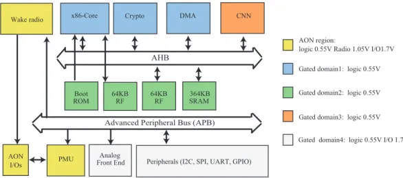
In [24], Pu et al. report the Black ghost SoC, one of the Qualcomm products, for IoT usage. This system is implemented with the TSMC 28-nm CMOS technology. Fig. 2.1 depicts a simplified block diagram of it. It includes a sensor control processor (ARM Cortex™-M0), energy efficient accelerators for specific applications (e.g. face recognition, voice word detection, etc), an analog front end (AFE) for sensing, a power management unit (PMU), a clock generation unit, and peripherals. The AFE is implemented as a sensor peripheral. It is composed of a low-noise sense amplifier buffer and 12-bit Analog Digital Converter (ADC). The M0 processor can process the input data from the AFE according to the timing defined by a software. Also, since recent complex applications (e.g image processing) require both high speed and low power computation, the data from AFE can be offloaded to the accelerators according to application requirements. The power consumption of these digital components can be tuned by the on-chip PMU. Moreover, all the power domain, except the always-on (AON) part, can be cut-off with on-chip switches. As a result, this SoC can be driven by a tiny Li-Ion battery.
From Intel, Karnik et al. disclosed a self-powered IoT edge SoC in 14-nm Tri-Gate CMOS technology [33]. Fig. 2.2 describes a conceptual block diagram of this SoC. It inte-grates an x86 host application processor, a convolutional neural network (CNN) accelerator for visual recognition and classification, a crypto engine for secure boot and data
ARM Cortex-M0 SRAM Peripheral (UART SPI I2S I2C) Always -on Domain (AON) (Interrupt, RTC Timer, Power control) PMU High-performance Bus Network-on-Chip (NoC)
DSP Processor SRAM Vision Processor SRAM
Accelerators Sensor control processor
Clock generator (PLL, RC relaxation oscillator) Analog frontend (Amplifier, ADC) Low dropout regurator Switch mode power supply
Voltage from Off chip Li-Ion battery
Nearthreshold voltage for logics (e.g. 0.55V) Voltage for memory (e.g. 0.75V)
1.05V region 1.8V for analog circuits
Figure 2.1: Simplified block diagram ofBlack ghostarchitecture
Wake radio x86-Core Crypto DMA CNN
AHB Boot ROM 64KB RF 64KB RF 364KB SRAM
Advanced Peripheral Bus (APB)
AON
I/Os PMU Peripherals (I2C, SPI, UART, GPIO) Analog
Front End
AON region:
logic 0.55V Radio 1.05V I/O1.7V Gated domain1: logic 0.55V
Gated domain2: logic 0.55V
Gated domain3: logic 0.55V
Gated domain4: logic 0.55V I/O 1.7V
Figure 2.2: Simplified block diagram of the self-powered IoT edge from Intel
sion among IoT nodes and gateways, a sub-mW radio receiver for the control signals from IoT gateways, an analog front end, 512KB shared memory, and on-chip power management unit. Similarly to theBlack ghostSoC, the x86 processor and accelerators can treat the data from the AFE. Also, since CNN is one of the promising techniques for energy efficient and high-performance image processing, it is implemented as the accelerator. Moreover, the equipped crypto engine can protect each IoT edge from malicious network attacks. At the active state of the SoC, the sensor, image data capture, image recognition/classification, or BLE transmission can be conducted. On the other hand, at the standby mode, all of the
2.1. System on Chip 11 Rocket Core 16KB Scalar Inst.Cache Vector Accelerator 16KB Vector Inst.Cache PMU (Body bias controller is also equipped)
32KB Shared Data.Cache
Arbiter
Clock generator
Async. FIFO/ Level shifters between domains
Core region voltage for logics (e.g. 0.55V)
Uncore region: 1.0V, 1.8V
Figure 2.3: Simplified block diagram of the RISC-V SoC
subsystems, except the AON part, can be power-gated with the PMU. As a result, this plat-form can perplat-form an image capture application with 24mW of the power consumption at maximum, which can be driven by a tiny battery.
Keller et al. reported a RISC-V processor SoC in 28-nm FD-SOI CMOS technology [35]. Fig. 2.3 shows a block diagram of the RISC-V SoC.Rocket, which is a 64-bit in-order single-issue processor supporting open RISC-V instruction set, is adopted. Also, a vector accelerator is implemented for compute-intensive workloads. Although this SoC does not include an AFE which can connect to off-chip sensors, an on-chip power management, and clock generator unit are integrated. The power management unit of this SoC can tune the processor’s body biases and power supply voltage.
In [36], a fully integrated battery-powered system-on-chip in 40-nm CMOS, named Brain SoC, is reported. This SoC is used for controlling an insect-scale pico-aerial vehicle (Fig. 2.4). For such applications, low-power VLSI systems are important because available power budget is quite restricted. Indeed, a take-off mass of a tiny aerial vehicle is poor, thus, a tiny battery can be available. TheBrain SoCis composed of general-purpose cores (Cortex M0 and Siskiyou Peak), accelerators (for Convolution filter and image interpolation optical flow(IIOF)), a digital signal processing (DSP) unit, memory components, on-chip voltage regulators, I/Os, ADCs, and an actuator controller for pico-aerial vehicle’s wing. To perform efficient computations, a heterogeneous architecture is adopted like the other SoCs. The accelerators and DSP can be accessed by the general-purpose cores via the memory mapped registers. According to the computation results from these components, the actuator controller outputs control signals. The on-chip voltage regulator down-converts the battery output voltage because it is much higher than the maximum available voltage for the on-chip transistors. The core and accelerators can operate with 7.5mW of power consumption at 0.63V of power supply voltage. Nevertheless, the leakage current occupies
Cortex M0
AHB
System Memory
APB
Peripherals (I2C, SPI, GPIO)
Interrupt Controller Analog domain:1.8V Digital domain: 0.6-0.9V Image Memory DSP Memory Siskiyou Peak DSP Engine IIOF Conv Filter
Memory Mapped Registers ADC
Actuator
Controller Power controller domain: 3.7V
from an off-chip battery On-chip voltage regulator
Figure 2.4: Simplified block diagram of the BrainSoC
ARM Cortex-M0+
AHB Lite Bus
VREG power domain AON 1.2V analog domain
DMA Debug
Other peripherals (ROM, AES128, SPI)
MBIST 4+4KB SRAM 4KB SRAM Clock Gen. Performance monitor Async interface Shadow RTC PMU Master RTC
Figure 2.5: Simplified block diagram of the near threshold SoC in [37]
the large portion of the total current (3.3mW at this condition).
The work presented in [37] reports a tiny microcontroller in 65-nm CMOS for IoT ap-plications (Fig. 2.5). This SoC consists of a CPU (Cortex-M0+ including DMA controller), 12KB RAM, a clock generator, a performance monitor, a PMU, and peripherals. As can be expected by the implemented computation budget, target applications of this SoC are smaller than those of the other SoCs reviewed so far. Nevertheless, the on-chip configura-tion is adopted for the PUM. The PMU can dynamically control the power supply voltage for the VREG power domain, shaded in blue shaded in Fig. 2.5. The VREG voltage domain
2.2. Power consumption on CMOS VLSI 13
is divided into 16 power sub-domains for flexible voltage control. This SoC also enables a power gating technique similarly to [33]. By utilizing the dynamic voltage/frequency con-trol and the power gating, the energy efficiency of this SoC is much improved. Indeed, the average power consumption with the low-power IoT workloads (EEMBC’s ULPBench) is 1.01µW.
Firstly, we can notice that matured process technology is actually used for embedded VLSI systems as stated in the trend ofMore than Moore. In fact, the studies in [36] and [37] respectively adopt 40-nm and 65-nm technologies even though more scaled ones are avail-able. Nevertheless, as briefly explained in the previous chapter, these mature technologies are scaled enough to cause some detrimental effects such as leakage current and process variation. Also, according to the transistor scaling trend, smaller feature size technologies than 28-nm can be considered as mature in the future. Indeed, a 14-nm process technol-ogy has actually matured; thus, the work [33] adopts it. From this context, the detrimental effects caused by the scaling will be a more fatal problem for low-power VLSI designs. Therefore, an efficient way to suppress these effects is required.
Also, some of the recent SoCs are often equipped with large computation systems (i.e. a processor + accelerators) even for embedded systems. Needless to say, integrating more transistors causes more leakage current. In addition, when VLSI systems operate, the dy-namic power is consumed as explained later. Larger computation resource incurs larger dynamic power similarly to the leakage current. Therefore, the power management for re-cent VLSI systems needs to consider not only the leakage but dynamic power as well. Note that, regarding the reviewed SoCs, the power management should be integrated inside a chip.
2.2
Power consumption on CMOS VLSI
In order to discuss how to control the VLSI power efficiently, we need to know its basic characteristics. Generally speaking, the power consumption of CMOS VLSI is composed of the dynamic (Pdy) and static power (Pst) as follows:
Ptotal =Pdy+Pst (2.1)
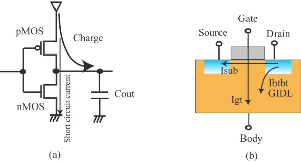
The dynamic power is consumed by charging and discharging parasitic capacitors for signal transition as depicted in Fig. 2.6 (a). On the other hand, the static power is consumed by the leakage current even when the transistor is cut-off. These two power phenomena have different characteristics; therefore, the characteristics of the dynamic power are firstly explained hereafter.
2.2.1 Dynamic power
As briefly explained, the dynamic power is caused when MOSFETs charge/discharge par-asitic capacitors. The current consumption here is referred to as switching current. There-fore, similarly to the equations for charged energy at capacitors, the power consumption from switching current can be formulated as:
Here,αat is switching activity, C is capacitance,f is operational frequency, and VDD is
power supply voltage. Also, the dynamic current includes internal the short circuit current, which flows from the power supply terminal to ground when the input signal transits and weakly turns-on both nMOSFET and pMOSFET. The dynamic power is inevitable for com-putation. Also, higher switching activity incurs higher power consumption. Therefore, the large VLSI systems such as [24, 33, 35] suffer from large dynamic power.
The dynamic power consumption can be suppressed by lowering the power supply volt-age as depicted in Fig. 2.7 (a). Nevertheless, as explained later, there is a trade-off between the gate delay and power consumption when controlling the voltage. This trade-off makes the voltage control complex.
In the next subsection, the characteristics of the leakage current are explained.
Cout
Charge
pMOS
nMOS
(a)
Gate
Drain
Source
Isub
Igt
Body
Ibtbt
GIDL
(b)
Short circuit current
Figure 2.6: Power consumption on CMOS VLSI (a) Dynamic current (b) Leakage current
2.2.2 Static power
The so-called “static power” is caused by the sub-threshold leakage current, gate leakage current, gate induced drain leakage (GIDL) and p-n junction leakage current in MOSFETs [13] (Fig. 2.6 (b)). These can be ignored before the technology nodes of 250nm. However, from the node of 180nm, their effects are drastically strengthened and have to be taken into consideration.
Sub-threshold leakage (Isub) is a drain-source current even when a transistor is at a
cut-off state. Unlike the current at a super threshold region dominated by the drift effect,Isubis
caused by diffusion current [38]. (Isub) can be formulated by the following equation:
Isub=Iof f10
Vgs+η(Vds−VDD)+Kγ Vsb
S (1−e
−Vds
2.2. Power consumption on CMOS VLSI 15 V DD
Logic
(b)
Logic
(a)
VBP VBNFigure 2.7: Voltage control technique: (a) Power supply control (b) Body bias control
WhereIof f is the sub-threshold leakage current atVds=VDD,Vgs=0V, and zero bias. vT is
the thermal voltage,ηis the DIBL coefficient,Kγis the coefficient of body bias controlling,
andSis the sub-threshold slope [13].
The gate leakage current (Igt) is caused by the tunnel effect. That is, the electron in the
gate terminal is released to the channel if the gate oxide is very thin. (Igt) can be represented
as: Igt=W PA( VDD tox )2e−PBVDDtox (2.4) where tox is the thickness of the gate oxide, W is the gate width, and PA and PB are
constants determined by the process technology [13].
The pn-junction leakage current is observed at the parasitic diodes in a MOSFET. Al-though this leakage current is not a serious problem in most cases, it cannot be ignored at the drain terminal because of its high impurity density. The high density causes a band to band tunnel current (IBT BT).IBT BT can be formulated as:
IBT BT =W XjP1( Ej Eg) VDDe −P2E 1 g .5 Ej (2.5)
whereXjis the junction depth of the diffusion,Egis the bandgap voltage,Ej is the electric
field along the junction, andP1andP2are technology constants [13].
GIDL occurs at a drain-gate overlap region when the gate is biased to form an accumu-lation layer at the silicon surface. This current is increased by the large potential difference between gate and drain because it enhances the electric field. As a result, a band-to-band current flows from the drain terminal.
In some cases, leakage current might occupy a large portion of the VLSI power con-sumption. For example, Fig. 2.8 show the breakdown of the power consumption of a real chip processor V850 fabricated with SOTB 65-nm CMOS technologies [39]. As can be seen from the graph, the leakage current consumes 64.6% of the power consumption in the
0 1 2 3 4 5 6 7 8 9 10 Current consumption [mA ] Leak Dynamic VDD=0.4V 37MHz Zero bias 64.6% V850
Figure 2.8: Break down of the power consumption
case of V850. In other words, the great portion of the power is wasted at V850; thus, an efficient solution to reduce the leakage current is required.
It is important to mention that using low-leakage devices (e.g. long-channel devices) is not the panacea for all low-power applications. This is because such transistors often require highVDD voltages. This incurs larger dynamic power consumptions as depicted in
equation (2.2). Also, the mandatory use of a highVDD can limit the number of potential
target applications. For example, bio-sensor platforms sometime need to operate under the power budget of biofuel cells, which can output around 0.4V as depicted in [40]. This voltage region is too low to adopt low-leakage devices. Therefore, it is still necessary to develop leakage reduction techniques for leaky process technologies.
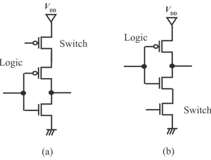
It is also worth noting that power gating (PG) is one of the most well-known leakage reduction techniques. The essential idea of PG is to turn-off unused circuits with switch transistors as depicted in Fig. 2.9. Since the off resistance is much increased due to the switches, the leakage current can be drastically reduced when a target system is in a standby state. Nevertheless, this technique clearly cannot be used for active state circuits because the power supply is disconnected. Therefore, the PG cannot also be the solution for all low-power applications.
2.2.3 Power and delay trade-off
Contrary to PG, lowering the power supply voltage can reduce both of the leakage and switching current at an active state. That is why, recent SoCs often operate at a near thresh-old voltages [23,24,33,35]: At a conventional voltage region, around 1.0 V of power supply voltage is used, while it is decreased to roughly 0.5V in the near threshold voltage region.
2.2. Power consumption on CMOS VLSI 17 V DD
Logic
Switch
(b)
(a)
V DDLogic
Switch
Figure 2.9: Power gating: (a) header switch (b) footer switch
Nevertheless, when the power supply is controlled, the gate delay should also be taken into consideration as can be seen in the alpha power law [41]. In this law, the delay is given by:
td=x
VDD
(VDD−VT H)α
(2.6)
wherexis a process parameter and αis a parameter for velocity saturation at highVDD.
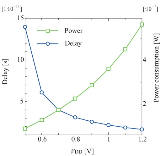
Sinceαis from 1 to 2, we can notice that lower voltages cause large gate delays. The trade-off between the power and gate delay can be graphically understood with Fig. 2.10, which depicts theVDD dependency to the power and delay of an inverter gate implemented with
SOTB 65-nm technology.
For a standby state of VLSI systems which does not require any computations, a very low-power (and slow) state can be used. On the other hand, for an active state where a given VLSI system has to operate at a certain frequency, its voltage has to be carefully chosen. Otherwise, considering the trade-off, excessive power is consumed.
On the condition that the trade-off is utilized properly, the VLSI power consumption can be drastically reduced by adopting dynamic voltage and frequency (DVFS) scaling. That is, according to various performance demands, the supplied voltage and frequency are adaptively scaled. The power management units in [24, 35] enable DVFS. For example, in [35], the power supply voltage level can be selected from the four values. Also, theBlack ghostSoC [24] enables the voltage control with 12.5mV of the voltage step.
In addition to the power supply voltage control, body bias control (BBC) can also re-alize a trade-off between the standby power and gate delay. Although the required power management becomes more complex, the energy efficiency of VLSI systems can be much improved by adopting both power supply and body bias control.
0.6
0.8
1
1.2
5
10
15
[1·10
−11]
2
4
[·10
−7]
V
DD[V]
Delay [s]
Power consumption [W]
Power
Delay
Figure 2.10: Trade-off between the power consumption and gate delay (f = 200M Hz)
2.3
Body bias control
BBC consists of manipulating the body voltages (See Fig. 2.7 (b) and Fig. 2.6 (b)) of a MOS transistor to adjust its threshold voltage after chip fabrication. In order to control the body voltage, additional layers called “well” are added between the substrate and transistor.1 Therefore, BBC controls the voltage of well layers.
VT H is defined as the gate voltage which can achieve 2ΦB of the silicon surface
po-tential. Here, ΦB is the difference between Fermi potential and intrinsic potential [38].
Considering the MOSFET structure, when the well voltages of MOSFETs are controlled, the potential of the silicon surface is affected, hence, VT H can also be changed. VT H is
formulated as: VT H =Vt0+γ( p φs+Vsb− p φs) (2.7)
where Vt0 is the threshold voltage when the source-body voltage (Vsb) is 0, and γ is a
1The well is conventionally used for optimizing impurity density. But, it can also be exploited for insulating
2.4. Fully Depleted Silicon on Insulator 19
Table 2.1: Summary of body bias control
pMOSFET nMOSFET Effect
Reverse bias VS <VBP VS >VBN Low leakage & Low speed
Forward bias VS >VBP VS <VBN High speed & High leakage
Zero bias VS=VBP VS= VBN Normal threshold voltage
coefficient for the body bias effect. Here,φsis
φs=vTln(
NA
ni
) (2.8)
whereNAis the doping level in the channel, andniis the intrinsic carrier concentration in
undoped silicon.
As depicted in equation (2.3), the body voltage affects the sub-threshold leakage current. This makes a trade-off between the leakage current and gate delay. From the viewpoint of this trade-off, the BBC can be categorized into three states. When the well voltage for nMOS (V BN) is lower than the source voltage and the well voltage for pMOS (V BP) is higher than the source voltage (VSp),VT H is increased. This state is referred to as Reverse
Body Bias (RBB). RBB can suppress the sub-threshold leakage current at the cost of the gate delay. On the other hand, whenV BN(V BP) is higher (lower) thanVSn(VSp),VT H
is decreased. This state is called Forward Body Bias (FBB). FBB can reduce the gate delay; but, the leakage current is exponentially increased. When the body bias is shorted to the source voltage,VT H does not shift from a nominal voltage decided by the manufacturing
process. This state is called zero bias. Fig. 2.11 shows the trade-off which is obtained by an inverter cell simulation with SOTB 65-nm technology. In this graph, we assume that the supplied body bias is set to the same magnitude between nMOS and pMOS. When 0.2V of FBB is supplied, the gate delay is reduced by 16.8% compared to the zero bias condition; but the leakage current is 2.68 times higher. While 0.5V of RBB can decrease the leakage current by 88.0%, the gate delay is stretched 1.61 times. Conventionally, BBC has been adopted to reduce the leakage power [14, 15] and improve system performances [42].
Similarly to the power supply voltage control, when a system is in a standby mode, a strong reverse bias can be applied to reduce the leakage current. On the other hand, when a system needs to operate at a certain performance, the body bias voltages have to be also carefully chosen for each performance requirement.
For low-power VLSI designs, utilizing BBC has become more important because novel Fully Depleted Silicon on Insulators (FD-SOI) can enhance the body bias effect as discussed in the next section.
2.4
Fully Depleted Silicon on Insulator
As the name suggests, FD-SOI is formed on an insulation layer and its transistor body is fully depleted. Recent FD-SOIs enable BBC as observed in UTBB [20, 43] and SOTB [21, 44] technologies because the nMOSFET and pMOSFET are formed on the ultra thin
−0.4
−0.2
0
0.2
0
1
[
·
10
−9]
4
6
[
·
10
−11]
Delay [s]
Body bias [V]
Leakage current [A]
Delay
Leakage current
RBB
FBB
Figure 2.11: Body bias effect simulation.
BOX layer (Fig. 2.12 (a)). Although the conventional bulk technology suffers from the p-n leakage current between the drain and source to the body, the BOX layer can remove it. Consequently, it ensures higher leakage reduction and more efficient body bias control than other conventional MOSFETs.
Thanks to the advantage of body biasing on FD-SOI, a lot of research have been con-ducted to exploit its benefits. For example, the RISC-V SoC [35] explained in the early part of this chapter is equipped with a body bias controller. Thanks to the BBC, the maximum operational frequency of this SoC (0.9V ofVDD) is improved from roughly 500MHz (zero
bias) to 600MHz (1.0V of FBB). Also, in [45], a DSP is implemented with 28-nm FD-SOI technology. It achieved 460MHz at 0.397V ofVDD and 2V of FBB. In other words, even
with a near threshold voltage is used, roughly 500MHz of operational frequency can be performed with the body bias. FBB is also effective for a super threshold region such as 1.2V. In fact, an ARM Cortex™A9 processor fabricated with a 28-nm FD-SOI technology achieved 2.6GHz of operational frequency at 0.6V of FBB. Moreover, as observed in [16] which is based on 65-nm FD-SOI technology, strong reverse bias is utilized. The imple-mented microcontroller in [16] recorded 140nA of sleep current at 0.35V ofVDDand 2.5V
2.5. Process variation 21
P-sub
N-well
P-well
STIDeep n-well
BOXlayer
P-sub
N-well
P-well
STIDeep n-well
pMOSFET nMOSFET
(b)
(a)
Figure 2.12: Cross-sectional view of MOSFET: (a) FD-SOI (b) Bulk.
of RBB. In addition, by appropriately considering the traoff between the power and de-lay, the operating energy efficiency can be improved. In [46], an accelerator implemented with 65-nm FD-SOI technology achieved 192MOPS(Mega Operations Per Second)/mW.
In addition to the advantages obtained with BBC, the FD-SOI structure can adopt a dopantless technique for the channel because the device scaling of FD-SOIs is dominated by the thickness of the transistor body on the insulator [38]. This dopantless strategy can suppress the variation when compared to the conventional bulk technologies as explained later. However, the process variation problem still remains even when the FD-SOI tech-nologies are used. The next section is dedicated to explore the characteristics of the process variation.
2.5
Process variation
Even if a chip is designed with certain parameters, fabricated one might have different characteristics. This fabrication uncertainty is also an obstacle to recent scaled process technologies because it degrades both chip yield and energy efficiency of VLSI systems. In order to understand why it degrades the energy efficiency, we consider, for example, that a huge number of chips are fabricated with a certain design and they should operate at a given performance requirement. If the chips are designed with optimistic parameters, some chips cannot perform the target frequency. Therefore, in general, the worst case parameters are used for VLSI system designs to improve the chip yield. However, since such case rarely occurs, the design is excessive in most cases. In other words, the supplied voltage for them
is excessive. This results in large power overheads.
The most dominant factors of the device level variation are deviations of transistor chan-nel length and threshold voltage (VT H) [13]. Gate length varies from designed patterns due
to across chip linewidth variation (ACLV) and line edge roughness (LER). ACLV is caused by lithography limitations and etching deviation depending on each layout pattern. Since recent lithographies need to fabricate smaller feature size device than the used wavelength, it is difficult to completely realize a given layout design. Also, the etching rate depends on the polysilicon density. When the density is increased, the etch rate is decreased. Contrary to ACLV, the reason of LER is not elucidated, to the best of author’s knowledge, and occurs randomly. However, at highly scaled technology, it is one of the dominant variation sources. Indeed, the average variation from LER reaches 4nm at a 35-nm process [47].
The threshold voltage is a function of the number of impurities on the channel as de-picted in equation (2.7). That is why inaccuracies of impurity doping causeVT Hvariations.
This effect is called as random dopant fluctuation (RDF). The standard deviation ofVT H
under RDF is formulated as:
σVt = tox ox × 4 p q3 siφbNa √ 2LW (2.9)
whereNais the impurity density,siis equal to11.80, andφbis the surface potential. As
can be seen from this equation, a smallerLandW result in larger threshold variation. In other words, smaller transistors (i.e. highly scaled transistors) cause large process varia-tions.
Fabricated metal wires connecting each transistor also have variations. Similarly to the gate length variation, the fabrication accuracy relies on lithography limitations and the etching deviation depends on each layout pattern. Also, the thickness of the wires and the resistance of the contacts vary due to the fabrication inaccuracy. These phenomena also affect the delay and leakage characteristics of fabricated VLSI systems.
Considering its dopantless structure, FD-SOI is one of the low variation devices as explained before. This is because the impurity density is related to the threshold voltage variation but this doping step is skipped. As a result, the random variation can be mitigated. Indeed, although the random process variation raises the minimum operational voltage for SRAMs with conventional bulk technologies, FD-SOI allows them to operate around 0.4V ofVDD [48]. Hence, FD-SOI devices are suitable for the current near-threshold computing
trend. In addition, due to the process simplicity, the fabrication cost is not so high compared to the bulk devices. This feature is also suitable for recent SoCs which requires low cost fabrication. Therefore, FD-SOI technology is a sensible choice for embedded systems. However, the process variation issues still remain even with the FD-SOI device.
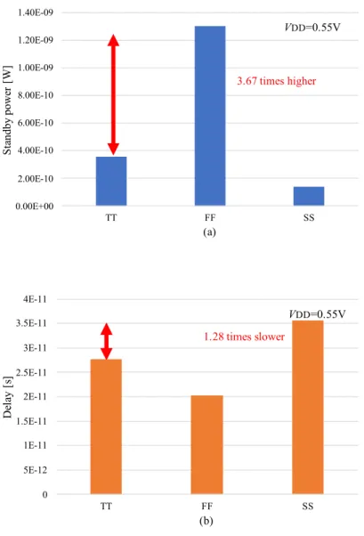
In order to show the variation problem on the FD-SOI device, Fig. 2.13 depicts the simulation results of the leakage current and gate delay on the various process variations. For this simulation, an inverter cell implemented with the SOTB 65-nm technology is used. Here, “F”, “T”, and “S” represent the slow, typical and fast transistor characteristics, re-spectively. “F” and “S” variations are given by the transistor which is the point of±3σin the normal distribution curve. As can be seen from the figures, FF condition incurs 3.67 times larger leakage current than that of TT. On the other hand, the gate delay is degraded
2.6. On chip voltage generators 23
at the SS condition. Although FD-SOI is useful for low power VLSI systems, the process variation should be efficiently handled.
The BBC is an efficient mean not only for power management but suppressing the pro-cess variation as well [17–19]. Indeed, in [17], the standard deviation of the die frequency distribution is reduced by 7 times by applying the BBC. Therefore, when controlling the body bias, process variation effect should also be taken into consideration.
We have discussed that controlling the body biases and power supply voltage can effi-ciently suppress the power consumption. Also, we have argued that process variations can be mitigated by body biasing. However, how to control these voltages? As explained in the early part of this chapter, on-chip power management units are often adopted as voltage controllers on recent SoCs. In the next section, on-chip voltage generators are reviewed.
2.6
On chip voltage generators
2.6.1 DC-DC converter for power supply
For the power supply of digital VLSI circuits, raw voltages from batteries are rarely used because it is too high for normal core transistors. The output voltage from a battery is usually down-converted to the level of standardVDDs by DC-DC converters. Three types of
DC-DC converters are often used for this purpose: Buck converter, Low drop-out regulator (LDO), and Switched capacitor.
The simplest buck converter is composed of switches, an inductor, and an output capac-itor as shown in Fig.2.14 (a). WhenS1is conducted andS2is cut-off, the power supplier charges the energy to the inductor. The diode is cut-off during this state, thus the charged energy can remain. When S1 is cut-off andS2 is on, the charged energy in the inductor is discharged to the load usingS2. Modulating the period when the switches are on and off, the output voltage (Vout) can be controlled. As shown in [49], the recent buck
con-verter allows the fine but discrete voltage control with 12.5mV of the step. Although this technique can provide the high conversion efficiency, it usually requires an off-chip induc-tor [49]. Otherwise, on-chip inducinduc-tors suffer from a large foot-print for implementation and low conversion efficiency [50].
An LDO is basically constructed with the pMOS switch, a comparator, and an output capacitor as shown in Fig.2.14 (b). Compared with the reference voltage, the output voltage is regulated to the required level. LDOs can enable fine voltage controllability such as 10mV of the voltage step [51]. However, the down-conversion of the voltage is performed with the on-resistance of the pMOS switch. This means that the conversion efficiency is linearly degraded when the output voltage is lowered. Hence, this way is clearly not suitable for near-threshold computing which requires quite low power supply voltages.
A switched capacitor converter is constructed with flying capacitors (Cfly), switches and an output capacitor as depicted in Fig.2.14 (c). The switches are periodically conducted with the complimentary oscillation signals (φandφ). By repeatedly charge and discharge the capacitor, the required voltage level can be obtained atVout. The depicted configuration
in this figure can down-convert the input voltage with the ratio of 2:1 under no output current. Indeed, whenφis “0”, the charged energy in the capacitor isCf lyVout, while it is
0.00E+00 2.00E-10 4.00E-10 6.00E-10 8.00E-10 1.00E-09 1.20E-09 1.40E-09 TT FF SS S ta ndby pow er [ W ] (a) VDD=0.55V 3.67 times higher 0 5E-12 1E-11 1.5E-11 2E-11 2.5E-11 3E-11 3.5E-11 4E-11 TT FF SS D el ay [s ] (b) VDD=0.55V 1.28 times slower
Figure 2.13: Process variation effects on a FD-SOI. The SOTB 65-nm technology is used. (nMOS/pMOS=FF,TT,SS): (a)Leakage power (b)Gate delay
2.6. On chip voltage generators 25 Logic Vin V out S1 S2 (a) Vref Vout Vin (b) + Vout (c) φ φ φ φ Vin Cfly
Figure 2.14: Various types of DCDC converters: (a) Buck converter (b) LDO (c) Switched capacitor.
output current,Cf lyVout =Cf ly(Vin−Vout)is obtained. As a result,Vout = 1/2Vincan
be obtained. The conversion ratio can be changed with the different number of switches and capacitors [52,53]. This converter can achieve both on-chip integration and high conversion efficiency at a low output voltage condition. Therefore, for a near-threshold voltage region, a switched capacitor type converter is often used and suitable for such demands. Nevertheless, the control granularity is not as high as the LDOs and buck converters. Indeed, in [35], only four voltage levels (1V, 0.9V, 0.67V and 0.5V) can be selected by users.
2.6.2 Voltage generators for BBC
Conventionally, on-chip body bias control schemes have been widely developed [14,54–58]. Kuroda et al.[14] proposed a system which can switch from strong reverse bias voltages, in the low leakage standby state, to a predefined body bias voltage in the operational state. This control is realized by monitoring the leakage current as shown in Fig. 2.15. The leakage current monitor can detect whether or not the leakage current reaches the predefined value. Based on the results, the charge pump is controlled and the body bias voltages are regulated. However, the system clock frequency needs to be decided and fixed before the chip implementation, so it cannot be changed afterward. Also, since the leakage current is sensitive to the process variation as previously discussed, this system also suffers from the variations. Therefore, it is not suitable as a body bias controller with recent process technologies.
In order to use various body bias voltages,Digital Analog Converters(DACs) are often used [54–57,59]. Fig. 2.16 shows a simplified diagram of a DAC-based body bias generator. The output voltage of the Charge Pump (CP) is compared with a reference voltage from
Leakage current monitor for Active mode
Leakage current monitor for Standby mode
Charge pump
VBN
VBP Target DCT processor
Figure 2.15: Simplified block diagram of VTCMOS.
the DAC. As a result, the body bias voltages are regulated to the same output voltages of the DAC. Note that, although a resistor ladder is depicted in this picture, another type such as a serial charge redistribution DAC can also be used [57]. Also, a resistor ladder can be inserted to the voltage feedback path, which is compared with the fixed reference voltage [59]. Recent body bias generators more or less utilize a DAC component.
It is obvious but important to mention that DAC-based body bias generators can output the voltage discretely. For example, in [55], n-well (p-well) voltage can be controlled with 58mV (72mV) of the step. Also, the body bias generator in [59] can enable 100mV of control granularity. Although the controller in [57] achieves 19mV of granularity, its power overhead is not suitable for low-power VLSI designs.
Thanks to the various level of output voltages, a DAC-based body bias generator can enable sophisticated body bias control. For example, a BBC system collaborating with a critical path monitor or/and variation monitor, which can detect a target system condition, is proposed in [54]. Fig. 2.17 depicts a simplified block diagram of it. The delay line is used as a variation monitor. The delay of the delay line is compared with the external clock signal. Then, the decoder sends the difference between these two signals. Based on this information, the body bias generator adjusts the output voltages on which a target system achieves a required performance.
The body bias control scheme in [60] also exploits a DAC-based configuration for com-plex voltage control. As previously mentioned, strong RBB conditions cause the increment of pn-junction leakage current and result in excessive power consumption. That is why the work presented in [60] adopts a current monitor circuit and can track the leakage optimal point.
From the above observations, used body bias voltages and power supply voltages should be properly decided. That is why a lot of research that tried optimizing them have been carried out in the past years. In the next section, previous works related to the optimization are reviewed.
2.7. Optimal voltage selection 27 BB Supplier VBP ={VBP1,...,VBPk} Target system VBN ={VBN1,...,VBNk} CP VBB Well sampler DAC
CHIP
BB SupplierFigure 2.16: Simplified diagram of a DAC-based body bias generator.
Delay line Decoder DAC-based BB gen. Target system VBP VBN Clock signal
Figure 2.17: Body bias tuning system using a DAC-based controller.
2.7
Optimal voltage selection
2.7.1 Energy optimization
One of the well-known ways of the optimization is to minimize the VLSI energy consump-tion [61, 62].
VLSI energy consumption at one cycle can be obtained by following equations:
Etotal=Cef fVDD2 +Wef fIsubVDDtd−cp (2.10)
whereWef f,Cef f, andtd−cprepresent a total effective gate width, a total effective parasitic
capacitor, and a total delay at the critical path. Since the dominant leakage current is usually the sub-threshold leakage current, this equation only considers it. The energy minimization is performed by solving this equation by selecting the power supply and threshold voltages properly. Calhoun et al. solved the equation (2.10) and served the optimal power supply voltage in [63].
The energy minimum point is often achieved at a sub or near threshold region. Gen-erally speaking, the maximum operational frequency is quite degraded in a sub threshold
![Figure 1.2: Minimum feature size scaling trend for Intel logic technologies [10]](https://thumb-ap.123doks.com/thumbv2/123dok/1878028.2665736/15.892.214.691.189.505/figure-minimum-feature-scaling-trend-intel-logic-technologies.webp)
![Figure 2.5: Simplified block diagram of the near threshold SoC in [37]](https://thumb-ap.123doks.com/thumbv2/123dok/1878028.2665736/24.892.143.746.163.473/figure-simplified-block-diagram-near-threshold-soc.webp)