iii
PERANCANGAN ALAT SERVICE BELL NIR-KABEL
Disusun Oleh :
Nama : Budi Hartono Ong
Nrp : 0622005
Jurusan Teknik Elektro, Fakultas Teknik, Universitas Kristen Maranatha,
Jl. Prof.Drg.Suria Sumantri, MPH no.65, Bandung, Indonesia.
Email : [email protected]
ABSTRAK
Teknologi wireless adalah teknologi yang sangat berkembang akhir-akhir ini. Hal ini dikarenakan kepraktisan yang ditawarkan oleh teknologi wireless yang tidak memerlukan kabel untuk koneksinya. Teknologi ini dapat diterapkan dalam berbagai aplikasi seperti telepon wireless, sistem central lock pada mobil, mainan remote control, dan masih banyak aplikasi lain yang digunakan untuk kepentingan pelayanan.
Pada Tugas Akhir ini, dirancang satu aplikasi teknologi wireless untuk keperluan pelayanan di tempat-tempat umum khususnya di restoran yang disebut dengan wireless service bell. Pada dasarnya sistem ini terdiri dari dua bagian utama yaitu perangkat pengirim dan penerima. Sistem yang dirancang terdiri dari banyak pengirim dan hanya satu penerima saja. Masing-masing perangkat pengirim akan mengirimkan informasi berupa alamat (yang berfungsi untuk membedakan perangkat pengirim yang satu dengan yang lain) dan data (yang berfungsi untuk membedakan pelayanan yang diminta, seperti meminta bill, menu, air, dsb.) yang dipicu melalui penekanan salah satu push button yang tersedia. Ketika push-button ditekan informasi (alamat dan data) akan dikodekan kemudian dikirimkan ke perangkat pengirim, yang selanjutnya akan ditransmisikan menggunakan gelombang radio 315MHz dengan modulasi ASK (Amplitude Shift Keying). Informasi yang dikirimkan akan diterima oleh perangkat penerima kemudian akan didekodekan untuk mendapatkan informasi sesungguhnya yang dikirimkan berupa alamat dan data. Selanjutnya informasi ini akan diolah oleh mikrokontroler Atmega16 untuk ditampilkan pada perangkat keluaran berupa LCD dan komputer.
Berdasarkan percobaan yang dilakukan, sistem wireless service bell yang dirancang berhasil direalisasikan dengan persentase keberhasilan 100% selama sistem masih berada di dalam batas jangkauan antenna. Jarak maksimum yang dapat dicapai di tempat terbuka (tidak ada halangan) adalah 30.6m dan di tempat tertutup (ada benda-benda pengahalang) adalah 15.2m.
Kata Kunci : Wireless Service Bell, ASK 315MHz, Pengontrol Mikro ATMega16
iv
THE DESIGNING OF WIRELESS SERVICE BELL
Composed by :
Name : Budi Hartono Ong
Nrp : 0622005
Electrical Engineering, Maranatha Cristian University,
Jl. Prof.Drg.Suria Sumantri, MPH no.65, Bandung, Indonesia.
Email : [email protected]
ABSTRACT
Now days, wireless technology is a highly developed technology. This is due to the practicality offered by wireless technology that does not require the use of wires. This technology can be applied in various applications such as wireless telephones, central lock system on cars, remote control for toys, and many other applications that are used for the benefit of the service.
In this final project, a wireless technology application will be designed for service in public places, especially in a restaurant which is called wireless service bell. Basically this system consists of two main parts: transmitter and receiver. The designed system consists of many transmitters and one receiver. Each transmitters will send the information in the form of address (which serves to distinguish the individual senders) and data (which serves to distinguish the requested services, such as requesting a bill, menu, water, etc..) that is triggered through suppression of one push-buttons. When the push-button is pressed, the information (address and data) will be encoded and then sent to the transmitter, which would then be transmitted using radio waves 315MHz with ASK (Amplitude Shift Keying) modulation. The information sent will be received by the receiver, then will be decoded to get the real information that is sent in the form of address and data. Further, the information will be processed by the microcontroller ATmega16 to be displayed on 2 output devices : LCD and computer.
Based on the experiments that have been conducted, the system which is designed for wireless service bell can be realized successfully with the successful percentage of 100% as long as the system is still inside the limit range of the antenna. The maximum distance that can be reached outdoors (without obstacle) is 30.6m and indoors (with multiple blocking objects) is 15.2m.
Key words : Wireless Service Bell, ASK 315MHz, ATMega16 Microcontroller
v
DAFTAR ISI
Halaman
ABSTRAK ... i
ABSTRACT ... ii
KATA PENGANTAR ... iii
DAFTAR ISI ... v
DAFTAR TABEL ... viii
DAFTAR GAMBAR ... ix
DAFTAR RUMUS ... xii
BAB I PENDAHULUAN I.1. Latar Belakang Masalah ... 1
I.2. Identifikasi Masalah ... 1
I.3. Perumusan Masalah ... 2
I.4. Tujuan ... 2
I.5. Batasan Masalah ... 2
I.6. Sistematika Penulisan ... 2
BAB II LANDASAN TEORI II.1. Frekuensi Gelombang Radio (RF/Radio Frequency) ... 4
II.1.1. Spektrum Gelombang Radio ... 4
II.2. Modulasi ... 6
II.3. Rangkaian Timer NE555 ... 7
II.3.1. Operasi Monostable IC NE555 ... 8
II.3.2. Operasi Astable IC NE555 ... 9
II.4. Gerbang Logika NOT (Inverter) ... 11
II.5. Pengkodean ... 12
II.5.1. IC HT12E ... 12
II.5.2. IC HT12D ... 16
vi
II.7. Mikrokontroler (µC) ... . 20
II.7.1. Fitur ATmega16 ... 20
II.7.2. Konfigurasi Pin ATmega16 ... 21
II.7.3. USART ... 24
II.7.3.1. IC MAX232 ... 28
II.7.4. Blok Diagram ATmega16 ... 28
BAB III PERANCANGAN DAN REALISASI III.1. Perancangan Sistem ... 30
III.2. Perancangan Hardware ... 33
III.2.1. Perancangan Hardware Untuk Transmitter ... 33
III.2.1.1. Perancangan Clock Monostable dengan IC NE555 ... 34
III.2.1.2. Perancangan Clock Astable dengan IC NE555 ... 36
III.2.1.3. Perancangan Encoder dengan IC HT12E ... 39
III.2.1.4. Perancangan Transmitter dengan Modul RF TLP-315. 41 III.2.2. Perancangan Hardware Untuk Receiver ... 41
III.2.2.1. Perancangan Receiver dengan Modul RF RLP-315 ... 42
III.2.2.2. Perancangan Decoder dengan IC HT12D ... 43
III.2.2.3. Perancangan Rangkaian Pengolahan Data dengan Mikrokontroler ATmega16 ... 45
III.3. Algoritma Pemrograman Sistem Wireless Service Bell ... 47
III.3.1. Diagram Alir Proses Pengolahan Data pada Receiver ... 47
III.3.2. Perancangan Program Interface Komputer ... 50
III.3.2.1. Diagram Alir Pengaktifan Komunikasi Serial ... 53
III.3.2.2. Diagram Alir Penerimaan dan Pengecekan Data ... 54
III.3.2.3. Diagram Alir Pengiriman Data Interrupt ke Mikrokontroler ... 55
III.3.2.4. Diagram Alir Penghentian Sistem ... 57
vii
IV.2. Pengamatan Sinyal pada Pin Output Monostable dan
Pin Output Inverter ... 60
IV.3. Pengamatan Sinyal pada Pin Output dari ClockAstable ... 61
IV.4. Pengamatan Sinyal pada Pin Output dari Encoder ... 63
IV.5. Pengamatan Sinyal Masukan Decoder pada Perangkat Receiver ... 64
IV.6. Pengamatan Sinyal pada Pin VT dan Pin Data dari IC Decoder ... 66
IV.7. Pengamatan Sinyal pada Pin Data dan Pin Output Inverter ... 67
IV.8. Output dari Sistem Wireless Service Bell ... 68
IV.8.1. Tampilan Output dari Address 1 dan Data 8 ... 69
IV.8.2. Tampilan Output dari Address 1 dan Data 9 ... 70
IV.8.3. Tampilan Output dari Address 2 dan Data 8 ... 71
IV.8.4. Tampilan Output dari Address 2 dan Data 9 ... 72
IV.8.5. Tampilan Output dari Address 3 dan Data 8 ... 73
IV.8.6. Tampilan Output dari Address 3 dan Data 9 ... 74
IV.9. Pengujian Jarak Maksimum Antara Transmitter dan Receiver di Ruang Terbuka (Outdoor) ... 76
IV.10. Pengujian Jarak Maksimum Antara Transmitter dan Receiver di Ruang Tertutup (Indoor) ... 78
IV.11. Analisis ... 80
BAB V KESIMPULAN DAN SARAN V.1. Kesimpulan ... 81
V.2. Saran ... 81
DAFTAR PUSTAKA
LAMPIRAN A FOTO WIRELESS SERVICE BELL
LAMPIRAN B SKEMATIK WIRELESS SERVICE BELL
LAMPIRAN C PROGRAM PADA PENGONTROL MIKRO ATMEGA16
LAMPIRAN D PROGRAM INTERFACING VB6
viii
DAFTAR TABEL
Halaman
Tabel 2.1 Pembagian Spektrum Gelombang Radio ... 5
Tabel 2.2 Tabel Kebenaran NOT ... 11
Tabel 2.3 Electrical characteristics IC HT12E ... 13
Tabel 2.4 Urutan pengiriman data IC HT12E ... 16
Tabel 2.5 Electrical characteristics IC HT12D ... 17
Tabel 2.6 Urutan penerimaan data IC HT12D ... ... 18
Tabel 2.7 Fungsi Khusus Port B ... 23
Tabel 2.8 Fungsi Khusus Port C ... 23
Tabel 2.9 Fungsi Khusus Port D ... 23
Tabel 2.10 Konfigurasi DB9 ... 26
Tabel 3.1 Pengaturan alamat dengan menggunakan DIP-SWITCH ... 40
Tabel 3.2 Pemberian input alamat oleh mikrokontroler ATmega16 ... 46
Tabel 3.3 Komponen dan properti ... 51
Tabel 4.1 Hasil pengujian jarak dan ketepatan data di ruang terbuka (outdoor) ... 76
ix
DAFTAR GAMBAR
Halaman
Gambar 2.1 Amplitude Shift Keying ... 7
Gambar 2.2 Susunan kaki IC timer NE555 ... 7
Gambar 2.3 Rangkaian Monostable IC NE555 ... 8
Gambar 2.4 Grafik hubungan antara R1 (RA), C ( ), dan nilai yang dihasilkan ... 9
Gambar 2.5 Rangkaian Astable IC NE555 ... 9
Gambar 2.6 Grafik hubungan antara R1 ( ), R2 ( ), C ( ), dan nilai yang dihasilkan ... 11
Gambar 2.7 Simbol gerbang logika NOT ... 11
Gambar 2.8 Konfigurasi kaki IC inverter 74LS04 ... 12
Gambar 2.9 Konfigurasi kaki IC HT12E ... 13
Gambar 2.10Grafik frekuensi osilasi vs tegangan power supply ... 15
Gambar 2.11Transmission timing IC HT12E ... 15
Gambar 2.12 Konfigurasi kaki IC HT12D ... 17
Gambar 2.13Grafik frekuensi osilasi vs tegangan power supply ... 19
Gambar 2.14 Konfigurasi modul RF TLP315 ... 19
Gambar 2.15 Konfigurasi modul RF RLP315 ... 20
Gambar 2.16 Konfigurasi Pin ATmega16 ... 22
Gambar 2.17 Contoh komunikasi asinkron ... 24
Gambar 2.18 Contoh sinyal di saluran ... 25
Gambar 2.19 Ilustrasi DCE dan DTE ... 26
Gambar 2.20 Konfigurasi kaki IC MAX-232 ... 28
Gambar 2.21 Blok Diagram ATmega16 ... 29
Gambar 3.1 Perancangan sistem perangkat transmitter ... 30
Gambar 3.2 Perancangan sistem perangkat receiver ... 30
Gambar 3.3 Output clock monostable ... 32
x
Gambar 3.5 Output inverter ... 32
Gambar 3.6 Perancagan hardware untuk transmitter ... 34
Gambar 3.7 Perancangan clock monostable ... 34
Gambar 3.8 Perancangan clock astable ... 36
Gambar 3.9 Perancangan encoder dengan IC HT12E ... 39
Gambar 3.10 Perancangan transmitter dengan modul RFTLP-315 ... 41
Gambar 3.11 Perancangan hardware untuk receiver ... 42
Gambar 3.12 Perancangan receiver dengan modul RFRLP-315 ... 43
Gambar 3.13 Perancangan decoder dengan IC HT12D ... 44
Gambar 3.14 Rangkaian pengolahan data dengan mikrokontroler ATmega16 ... 45
Gambar 3.15 Diagram alir proses pengolahan data pada receiver ... 48
Gambar 3.16 Perancangan interface komputer ... 51
Gambar 3.17 Diagram alir pengaktifan komunikasi serial ... 53
Gambar 3.18 Diagram alir penerimaan dan pengecekan data ... 54
Gambar 3.19 Diagram alir pengiriman data interrupt ke mikrokontroler .. 56
Gambar 3.20 Diagram alir penghentian sistem ... 57
Gambar 4.1 Bagian-bagian yang akan diamati pada sisi transmitter ... 58
Gambar 4.2 Bagian-bagian yang akan diamati pada sisi receiver ... 58
Gambar 4.3 Sinyal yang dihasilkan rangkaian clock monostable ... 59
Gambar 4.4 Sinyal output monostable (atas) dan sinyal output inverter (bawah) ... 60
Gambar 4.5 Sinyal keluaran yang dihasilkan rangkaian clock astable .... 62
Gambar 4.6 Hubungan antara clock monostable dan clock astable ... 62
Gambar 4.7 Sinyal keluaran dari pin output encoder ... 64
Gambar 4.8 Bentuk sinyal sesungguhnya dari pin output encoder ... 64
Gambar 4.9 Bentuk sinyal dari pin input decoder ketika belum ada data yang diterima ... 65
xi
Gambar 4.11 Bentuk sinyal data sesungguhnya yang masuk ke perangkat
Receiver ... 66 Gambar 4.12 Sinyal pada pin VT (atas) dan pin data (bawah) ... 67
Gambar 4.13 Bentuk sinyal pada pin data (atas) dan pin output inverter
(bawah) ... 68 Gambar 4.14 Tampilan awal pada media output komputer ... 69
Gambar 4.15 Tampilan awal pada media output LCD ... 69
Gambar 4.16 Tampilan permintaan bill oleh meja 1 pada media
komputer ... 70
Gambar 4.17 Tampilan permintaan bill oleh meja 1 pada media LCD ... 70
Gambar 4.18 Tampilan permintaan menu oleh meja 1 pada media
komputer ... 71
Gambar 4.19 Tampilan permintaan menu oleh meja 1 pada media LCD ... 71
Gambar 4.20 Tampilan permintaan bill oleh meja 2 pada media
komputer ... 72
Gambar 4.21 Tampilan permintaan bill oleh meja 2 pada media LCD ... 72
Gambar 4.22 Tampilan permintaan menu oleh meja 2 pada media
komputer ... 73
Gambar 4.23 Tampilan permintaan menu oleh meja 2 pada media LCD ... 73
Gambar 4.24 Tampilan permintaan bill oleh meja 3 pada media
komputer ... 74
Gambar 4.25 Tampilan permintaan bill oleh meja 3 pada media LCD ... 74
Gambar 4.26 Tampilan permintaan menu oleh meja 3 pada media
komputer ... 75
xii
DAFTAR RUMUS
Halaman
Rumus 2.1 ... 4
Rumus 2.2 ... 8
Rumus 2.3 ... 10
Rumus 2.4 ... 10
Rumus 2.5 ... 10
Rumus 2.6 ... 10
LAMPIRAN A
LAMPIRAN B
SKEMATIK WIRELESS SERVICE BELL
---
LAMPIRAN C
/***************************************************** This program was produced by the
CodeWizardAVR V1.25.3 Professional Automatic Program Generator
© Copyright 1998-2007 Pavel Haiduc, HP InfoTech s.r.l. http://www.hpinfotech.com
Project : Version : Date : 8/3/2010
Author : F4CG Company : F4CG Comments:
Chip type : ATmega16 Program type : Application Clock frequency : 11.059200 MHz Memory model : Small
External SRAM size : 0 Data Stack size : 256
*****************************************************/
#include <mega16.h> #include <delay.h>
// Alphanumeric LCD Module functions #asm
.equ __lcd_port=0x15 ;PORTC #endasm
#include <lcd.h>
#define RXB8 1 #define TXB8 0 #define UPE 2 #define OVR 3 #define FE 4 #define UDRE 5 #define RXC 7
#define FRAMING_ERROR (1<<FE) #define PARITY_ERROR (1<<UPE) #define DATA_OVERRUN (1<<OVR)
#define DATA_REGISTER_EMPTY (1<<UDRE) #define RX_COMPLETE (1<<RXC)
#if RX_BUFFER_SIZE<256
unsigned char rx_wr_index,rx_rd_index,rx_counter; #else
unsigned int rx_wr_index,rx_rd_index,rx_counter; #endif
// This flag is set on USART Receiver buffer overflow bit rx_buffer_overflow;
// USART Receiver interrupt service routine interrupt [USART_RXC] void usart_rx_isr(void) {
char status,data; status=UCSRA; data=UDR;
if ((status & (FRAMING_ERROR | PARITY_ERROR | DATA_OVERRUN))==0) {
rx_buffer[rx_wr_index]=data;
if (++rx_wr_index == RX_BUFFER_SIZE) rx_wr_index=0; if (++rx_counter == RX_BUFFER_SIZE)
{
rx_counter=0;
rx_buffer_overflow=1; };
};
if(data=='R') /*program penanganan data interrupt yang diperoleh untuk mereset LCD*/ {
lcd_clear(); }
}
#ifndef _DEBUG_TERMINAL_IO_
// Get a character from the USART Receiver buffer #define _ALTERNATE_GETCHAR_
#pragma used+ char getchar(void) {
char data;
while (rx_counter==0); data=rx_buffer[rx_rd_index];
if (++rx_rd_index == RX_BUFFER_SIZE) rx_rd_index=0; #asm("cli")
--rx_counter; #asm("sei") return data; }
#pragma used- #endif
#include <stdio.h>
// Declare your global variables here
void main(void) {
// Declare your local variables here
// Input/Output Ports initialization // Port A initialization
// Func7=In Func6=In Func5=In Func4=In Func3=In Func2=In Func1=In Func0=In // State7=T State6=T State5=T State4=T State3=T State2=T State1=T State0=T PORTA=0x00;
DDRA=0x00;
// Port B initialization
// Func7=Out Func6=Out Func5=Out Func4=Out Func3=Out Func2=Out Func1=Out Func0=Out
// State7=0 State6=0 State5=0 State4=0 State3=0 State2=0 State1=0 State0=0 PORTB=0x00;
DDRB=0xFF;
// Port C initialization
// Func7=In Func6=In Func5=In Func4=In Func3=In Func2=In Func1=In Func0=In // State7=T State6=T State5=T State4=T State3=T State2=T State1=T State0=T PORTC=0x00;
DDRC=0x00;
// Port D initialization
// Func7=In Func6=In Func5=In Func4=In Func3=In Func2=In Func1=In Func0=In // State7=T State6=T State5=T State4=T State3=T State2=T State1=T State0=T PORTD=0x00;
DDRD=0x00;
// Timer/Counter 0 initialization // Clock source: System Clock // Clock value: Timer 0 Stopped // Mode: Normal top=FFh // OC0 output: Disconnected TCCR0=0x00;
TCNT0=0x00; OCR0=0x00;
// Input Capture on Falling Edge // Timer 1 Overflow Interrupt: Off // Input Capture Interrupt: Off // Compare A Match Interrupt: Off // Compare B Match Interrupt: Off TCCR1A=0x00;
TCCR1B=0x00; TCNT1H=0x00; TCNT1L=0x00; ICR1H=0x00; ICR1L=0x00; OCR1AH=0x00; OCR1AL=0x00; OCR1BH=0x00; OCR1BL=0x00;
// Timer/Counter 2 initialization // Clock source: System Clock // Clock value: Timer 2 Stopped // Mode: Normal top=FFh // OC2 output: Disconnected ASSR=0x00;
TCCR2=0x00; TCNT2=0x00; OCR2=0x00;
// External Interrupt(s) initialization // INT0: Off
// INT1: Off // INT2: Off MCUCR=0x00; MCUCSR=0x00;
// Timer(s)/Counter(s) Interrupt(s) initialization TIMSK=0x00;
// USART initialization
// Communication Parameters: 8 Data, 1 Stop, No Parity // USART Receiver: On
// USART Transmitter: On // USART Mode: Asynchronous // USART Baud rate: 9600 UCSRA=0x00;
UCSRB=0x98; UCSRC=0x86; UBRRH=0x00; UBRRL=0x47;
// Analog Comparator Input Capture by Timer/Counter 1: Off ACSR=0x80;
SFIOR=0x00;
// LCD module initialization lcd_init(16);
// Global enable interrupts #asm("sei")
while (1) {
PORTB=0B11111110; /*program pengolah data pada receiver*/ if(PINA.4==1)
if(PINA.7==1) {
lcd_clear(); lcd_gotoxy(0,0);
lcd_putsf("MEJA 1 BILL"); printf("MEJA 1 BILL "); }
if(PINA.4==1) if(PINA.6==1) {
lcd_clear(); lcd_gotoxy(0,0);
lcd_putsf("MEJA 1 MENU"); printf("MEJA 1 MENU "); }
delay_ms(100); PORTB=0B11111101; if(PINA.4==1) if(PINA.7==1) {
lcd_clear(); lcd_gotoxy(0,0);
lcd_putsf("MEJA 2 BILL"); printf("MEJA 2 BILL "); }
if(PINA.4==1) if(PINA.6==1) {
lcd_clear(); lcd_gotoxy(0,0);
lcd_putsf("MEJA 2 MENU"); printf("MEJA 2 MENU "); }
PORTB=0B11111011; if(PINA.4==1) if(PINA.7==1) {
lcd_clear(); lcd_gotoxy(0,0);
lcd_putsf("MEJA 3 BILL"); printf("MEJA 3 BILL "); }
if(PINA.4==1) if(PINA.6==1) {
lcd_clear(); lcd_gotoxy(0,0);
lcd_putsf("MEJA 3 MENU"); printf("MEJA 3 MENU "); }
delay_ms(100);
if (PINA.5==0) {
lcd_clear(); }
LAMPIRAN D
Dim x As String /*menetukan tipe data dari variabel x sebagai string*/
Private Sub Command1_Click() /*program penghentian sistem bila button exit di klik*/ MSComm1.PortOpen = False
Unload Me End Sub
Private Sub Form_Load() /*program pengaktifan komunikasi serial*/ MSComm1.CommPort = 1
MSComm1.Settings = "9600,n,8,1" MSComm1.PortOpen = True List1.Clear
End Sub
Private Sub Image10_Click() /*program peresetan dan pengiriman interrupt ketika image10 diklik*/ Image3.Visible = False
Image2.Visible = False Image1.Visible = True Image10.Visible = False Text4.Visible = False Text5.Visible = False Timer2.Enabled = False Timer3.Enabled = False MSComm1.Output = "R" End Sub
Private Sub Image11_Click() /*program peresetan dan pengiriman interrupt ketika image11 diklik*/ Image5.Visible = False
MSComm1.Output = "R" End Sub
Private Sub Image12_Click() /*program peresetan dan pengiriman interrupt ketika image12 diklik*/ Image8.Visible = False
Image9.Visible = False Image7.Visible = True Image12.Visible = False Text8.Visible = False Text9.Visible = False Timer6.Enabled = False Timer7.Enabled = False MSComm1.Output = "R" End Sub
Private Sub Timer1_Timer() /*program penerimaan, pengecekan data, & pengaturan tampilannya*/ x = MSComm1.Input
If Len(x) > 0 Then
If Left(x, 11) = "MEJA 1 BILL" Then Image2.Visible = True
Image1.Visible = False Timer2.Enabled = True Image10.Visible = True Text4.Visible = True Text5.Visible = False End If
If Left(x, 11) = "MEJA 1 MENU" Then Image2.Visible = True
If Left(x, 11) = "MEJA 2 BILL" Then Image5.Visible = True
Image4.Visible = False Timer4.Enabled = True Image11.Visible = True Text6.Visible = True Text7.Visible = False End If
If Left(x, 11) = "MEJA 2 MENU" Then Image5.Visible = True
Image4.Visible = False Timer4.Enabled = True Image11.Visible = True Text7.Visible = True Text6.Visible = False End If
If Left(x, 11) = "MEJA 3 BILL" Then Image8.Visible = True
Image7.Visible = False Timer6.Enabled = True Image12.Visible = True Text8.Visible = True Text9.Visible = False End If
If Left(x, 11) = "MEJA 3 MENU" Then Image8.Visible = True
Image7.Visible = False Timer6.Enabled = True Image12.Visible = True Text9.Visible = True Text8.Visible = False End If
End Sub
Private Sub Timer2_Timer() /*program membuat image3 berkedip dengan selang waktu tertentu*/ Image3.Visible = True
Timer2.Enabled = False Timer3.Enabled = True End Sub
Private Sub Timer3_Timer() Image3.Visible = False Timer2.Enabled = True Timer3.Enabled = False End Sub
Private Sub Timer4_Timer() /*program membuat image6 berkedip dengan selang waktu tertentu*/ Image6.Visible = True
Timer4.Enabled = False Timer5.Enabled = True End Sub
Private Sub Timer5_Timer() Image6.Visible = False Timer5.Enabled = False Timer4.Enabled = True End Sub
Private Sub Timer6_Timer() /*program membuat image9 berkedip dengan selang waktu tertentu*/ Image9.Visible = True
Timer6.Enabled = False Timer7.Enabled = True End Sub
LAMPIRAN E
DATASHEET
---
2
12Series of Decoders
Selection Table
Function Address No.
Data
VT Oscillator Trigger Package Part No. No. Type
HT12D 8 4 L Ö RC oscillator DIN active²Hi² 18 DIP/20 SOP
HT12F 12 0 ¾ Ö RC oscillator DIN active²Hi² 18 DIP/20 SOP
Notes: Data type: L stands for latch type data output. VT can be used as a momentary data output.
1 July 12, 1999
General Description
The 212decoders are a series of CMOS LSIs for remote control system applications. They are paired with Holtek¢s 212series of encoders (re-fer to the encoder/decoder cross re(re-ference ta-b l e ) . F o r p r o p e r o p e r a t i o n , a p a i r o f encoder/decoder with the same number of ad-dresses and data format should be chosen.
The decoders receive serial addresses and data from a programmed 212series of encoders that are transmitted by a carrier using an RF or an IR transmission medium. They compare the se-rial input data three times continuously with
their local addresses. If no error or unmatched codes are found, the input data codes are de-coded and then transferred to the output pins. The VT pin also goes high to indicate a valid transmission.
The 212series of decoders are capable of decod-ing informations that consist of N bits of ad-dress and 12-N bits of data. Of this series, the HT12D is arranged to provide 8 address bits and 4 data bits, and HT12F is used to decode 12 bits of address information.
Features
· Operating voltage: 2.4V~12V
· Low power and high noise immunity CMOS technology
· Low standby current
· Capable of decoding 12 bits of information · Pair with Holtek¢s 212series of encoders · Binary address setting
· Received codes are checked 3 times
· Address/Data number combination - HT12D: 8 address bits and 4 data bits - HT12F: 12 address bits only
· Built-in oscillator needs only 5% resistor · Valid transmission indicator
· Easy interface with an RF or an infrared transmission medium
· Minimal external components
Applications
· Burglar alarm system · Smoke and fire alarm system · Garage door controllers · Car door controllers
· Car alarm system
· Security system · Cordless telephones
Block Diagram
Note: The address/data pins are available in various combinations (see the address/data table).
Pin Assignment
212Series of Decoders
2 July 12, 1999
D a t a S h i f t R e g i s t e r O s c i l l a t o r
B u f f e r
S y n c . D e t e c t o r
D i v i d e r
C o m p a r a t o r C o m p a r a t o r
B u f f e r T r a n s m i s s i o n G a t e C i r c u i t
D a t a D e t e c t o r
C o n t r o l L o g i c O S C 1
O S C 2
D I N
V D D V S S
V T D a t a L a t c h C i r c u i t
A d d r e s s
8 - A d d r e s s 4 - D a t a
1 2 - A d d r e s s 0 - D a t a
A 0 A 1 A 2 A 3 A 4 A 5 A 6 A 7 V S S
V D D V T O S C 1 O S C 2 D I N D 1 1 D 1 0 D 9 D 8 1 2 3 4 5 6 7 8 9 1 8 1 7 1 6 1 5 1 4 1 3 1 2 1 1 1 0
1 2 - A d d r e s s 0 - D a t a
A 0 A 1 A 2 A 3 A 4 A 5 A 6 A 7 V S S
V D D V T O S C 1 O S C 2 D I N A 1 1 A 1 0 A 9 A 8 1 2 3 4 5 6 7 8 9 1 8 1 7 1 6 1 5 1 4 1 3 1 2 1 1 1 0 1 2 3 4 5 6 7 8 9 1 0 2 0 1 9 1 8 1 7 1 6 1 5 1 4 1 3 1 2 1 1 N C V D D V T O S C 1 O S C 2 D I N A 1 1 A 1 0 A 9 A 8 N C A 0 A 1 A 2 A 3 A 4 A 5 A 6 A 7 V S S
8 - A d d r e s s 4 - D a t a
1 2 3 4 5 6 7 8 9 1 0 2 0 1 9 1 8 1 7 1 6 1 5 1 4 1 3 1 2 1 1 N C V D D V T O S C 1 O S C 2 D I N D 1 1 D 1 0 D 9 D 8 N C A 0 A 1 A 2 A 3 A 4 A 5 A 6 A 7 V S S
H T 1 2 F 2 0 S O P H T 1 2 F
1 8 D I P H T 1 2 D
1 8 D I P
Pin Description
Pin Name I/O Internal
Connection Description
A0~A11 I
NMOS TRANSMISSION
GATE
Input pins for address A0~A11 setting They can be externally set to VDD or VSS.
D8~D11 O CMOS OUT Output data pins
DIN I CMOS IN Serial data input pin
VT O CMOS OUT Valid transmission, active high
OSC1 I OSCILLATOR Oscillator input pin
OSC2 O OSCILLATOR Oscillator output pin
VSS I ¾ Negative power supply (GND)
VDD I ¾ Positive power supply
Approximate internal connection circuits
Absolute Maximum Ratings
Supply Voltage ...-0.3V to 13V Storage Temperature...-50°C to 125°C Input Voltage...VSS-0.3 to VDD+0.3V Operating Temperature ...-20°C to 75°C
Note: These are stress ratings only. Stresses exceeding the range specified under²Absolute Maxi-mum Ratings² may cause substantial damage to the device. Functional operation of this de-vice at other conditions beyond those listed in the specification is not implied and prolonged exposure to extreme conditions may affect device reliability.
212Series of Decoders
3 July 12, 1999
N M O S T R A N S M I S S I O N
G A T E
C M O S I N O S C I L L A T O R
O S C 1 O S C 2
C M O S O U T
Electrical Characteristics Ta=25°C
Symbol Parameter Test Conditions Min. Typ. Max. Unit
VDD Conditions
VDD Operating Voltage ¾ ¾ 2.4 5 12 V
ISTB Standby Current
5V
Oscillator stops ¾ 0.1 1 mA
12V ¾ 2 4 mA
IDD Operating Current 5V No loadf
OSC=150kHz ¾ 200 400 mA
IO
Data Output Source
Current (D8~D11) 5V VOH=4.5V -1 -1.6 ¾ mA
Data Output Sink
Current (D8~D11) 5V VOL=0.5V 1 1.6 ¾ mA
IVT
VT Output Source Current
5V VOH=4.5V -1 -1.6 ¾ mA
VT Output Sink Current VOL=0.5V 1 1.6 ¾ mA
VIH ²H²Input Voltage 5V ¾ 3.5 ¾ 5 V
VIL ²L²Input Voltage 5V ¾ 0 ¾ 1 V
fOSC Oscillator Frequency 5V ROSC=51kW ¾ 150 ¾ kHz
212Series of Decoders
212Series of Decoders
5 July 12, 1999
Functional Description
Operation
The 212series of decoders provides various com-binations of addresses and data pins in differ-ent packages so as to pair with the 212series of encoders.
The decoders receive data that are transmitted by an encoder and interpret the first N bits of code period as addresses and the last 12-N bits as data, where N is the address code number. A signal on the DIN pin activates the oscillator which in turn decodes the incoming address and data. The decoders will then check the re-ceived address three times continuously. If the received address codes all match the contents of the decoder¢s local address, the 12-N bits of data are decoded to activate the output pins and the VT pin is set high to indicate a valid transmission. This will last unless the address code is incorrect or no signal is received. The output of the VT pin is high only when the transmission is valid. Otherwise it is always low.
Output type
Of the 212series of decoders, the HT12F has no data output pin but its VT pin can be used as a momentary data output. The HT12D, on the other hand, provides 4 latch type data pins whose data remain unchanged until new data are received.
Part No.
Data Pins
Address Pins
Output Type
Operating Voltage
HT12D 4 8 Latch 2.4V~12V HT12F 0 12 ¾ 2.4V~12V
Flowchart
The oscillator is disabled in the standby state and activated when a logic²high²signal applies to the DIN pin. That is to say, the DIN should be kept low if there is no signal input.
Y e s C o d e i n ?
S t o r e d a t a N o
Y e s
N o
N o
N o
Y e s S t a n d b y m o d e
D i s a b l e V T & i g n o r e t h e r e s t o f
t h i s w o r d
Y e s
N o
Y e s A d d r e s s o r d a t a e r r o r ? L a t c h d a t a t o o u t p u t & a c t i v a t e V T A d d r e s s b i t s
m a t c h e d ?
M a t c h p r e v i o u s s t o r e d
d a t a ? P o w e r o n
Decoder timing
Encoder/Decoder cross reference table
Decoders
Part No. Data Pins Address Pins VT Pair Encoder
Package
Encoder Decoder
DIP SOP DIP SOP
HT12D 4 8 Ö HT12A 18 20 18 20
HT12E 18 20
HT12F 0 12 Ö HT12A 18 20 18 20
HT12E 18 20
Address/Data sequence
The following table provides address/data sequence for various models of the 212series of decoders. A correct device should be chosen according to the requirements of the individual addresses and data.
Part No. Address/Data Bits
0 1 2 3 4 5 6 7 8 9 10 11
HT12D A0 A1 A2 A3 A4 A5 A6 A7 D8 D9 D10 D11
HT12F A0 A1 A2 A3 A4 A5 A6 A7 A8 A9 A10 A11
212Series of Decoders
6 July 12, 1999
2 c l o c k s1 4
c h e c k
4 w o r d s 4 w o r d s
E n c o d e r D O U T
T r a n s m i t t e d C o n t i n u o u s l y < 1 w o r d
E n c o d e r T r a n s m i s s i o n E n a b l e
c h e c k D e c o d e r V T
L a t c h e d D a t a O u t
Oscillator frequency vs supply voltage
The recommended oscillator frequency is fOSCD(decoder)@50 fOSCE(HT12E encoder) @1
3fOSCE(HT12A encoder).
212Series of Decoders
7 July 12, 1999
f o s c ( S c a l e )
R o s c (W )
0 . 5 0 ( 1 0 0 k H z ) 1 . 0 0 1 . 5 0 2 . 0 0 2 . 5 0 3 . 5 0 4 . 0 0
3 . 0 0
0 . 2 5
2 3 4 5 6 7 8 9 1 0 1 1 1 2 1 3 V D D ( V D C )
6 8 k 6 2 k 5 6 k 5 1 k 4 7 k 4 3 k 3 9 k 3 6 k 3 3 k 3 0 k 2 7 k
7 5 k 8 2 k
1 0 0 k
1 2 0 k
Application Circuits
Notes: Typical infrared receiver: PIC-12043T/PIC-12043S (KODESHI CORP.) or LTM9052 (LITEON CORP.)
Typical RF receiver: JR-200 (JUWA CORP.)
RE-99 (MING MICROSYSTEM, U.S.A.)
212Series of Decoders
8 July 12, 1999
R e c e i v e r C i r c u i t
H T 1 2 D
A 0
A 1 A 2
A 3
A 4
A 5
A 6
A 7 V S S
V D D V T
O S C 1
O S C 2
D I N
D 1 1
D 1 0 D 9
D 8
1
2
3
4
5
6
7
8
9
1 8
1 7 1 6
1 5
1 4
1 3
1 2
1 1 1 0
R O S C
V D D
R e c e i v e r C i r c u i t
H T 1 2 F
A 0 A 1
A 2
A 3 A 4
A 5
A 6 A 7
V S S V D D
V T
O S C 1
O S C 2 D I N
A 1 1
A 1 0 A 9
A 8
1
2
3
4
5
6
7
8
9
1 8
1 7
1 6
1 5
1 4
1 3
1 2
1 1
1 0
R O S C
212Series of Decoders
9 July 12, 1999
Copyrightã1999 by HOLTEK SEMICONDUCTOR INC.
The information appearing in this Data Sheet is believed to be accurate at the time of publication. However, Holtek assumes no responsibility arising from the use of the specifications described. The applications mentioned herein are used solely for the purpose of illustration and Holtek makes no warranty or representation that such applications will be suitable without further modification, nor recommends the use of its products for application that may pres-ent a risk to human life due to malfunction or otherwise. Holtek reserves the right to alter its products without prior notification. For the most up-to-date information, please visit our web site at http://www.holtek.com.tw.
Holtek Semiconductor Inc. (Headquarters)
No.3 Creation Rd. II, Science-based Industrial Park, Hsinchu, Taiwan, R.O.C. Tel: 886-3-563-1999
Fax: 886-3-563-1189
Holtek Semiconductor Inc. (Taipei Office)
5F, No.576, Sec.7 Chung Hsiao E. Rd., Taipei, Taiwan, R.O.C. Tel: 886-2-2782-9635
Fax: 886-2-2782-9636
Fax: 886-2-2782-7128 (International sales hotline)
Holtek Microelectronics Enterprises Ltd.
RM.711, Tower 2, Cheung Sha Wan Plaza, 833 Cheung Sha Wan Rd., Kowloon, Hong Kong Tel: 852-2-745-8288
This datasheet has been downloaded from:
www.DatasheetCatalog.com
HT12A/HT12E
2
12Series of Encoders
Selection Table
Function Address No.
Address/ Data No.
Data
No. Oscillator Trigger Package
Carrier Output
Negative Polarity Part No.
HT12A 8 0 4 455kHz
resonator D8~D11
18 DIP
20 SOP 38kHz No
HT12E 8 4 0 RC
oscillator TE
18 DIP
20 SOP No No
Note: Address/Data represents pins that can be address or data according to the decoder require-ment.
1 April 11, 2000
General Description
The 212encoders are a series of CMOS LSIs for remote control system applications. They are capable of encoding information which consists of N address bits and 12-N data bits. Each ad-dress/data input can be set to one of the two logic states. The programmed addresses/data are transmitted together with the header bits
via an RF or an infrared transmission medium upon receipt of a trigger signal. The capability to select a TE trigger on the HT12E or a DATA trigger on the HT12A further enhances the ap-plication flexibility of the 212series of encoders. The HT12A additionally provides a 38kHz car-rier for infrared systems.
Features
· Operating voltage
- 2.4V~5V for the HT12A - 2.4V~12V for the HT12E
· Low power and high noise immunity CMOS technology
· Low standby current: 0.1mA (typ.) at VDD=5V
· HT12A with a 38kHz carrier for infrared transmission medium
· Minimum transmission word
- Four words for the HT12E - One word for the HT12A
· Built-in oscillator needs only 5% resistor
· Data code has positive polarity
· Minimal external components
· HT12A/E: 18-pin DIP/20-pin SOP package
Applications
· Burglar alarm system
· Smoke and fire alarm system
· Garage door controllers
· Car door controllers
· Car alarm system
· Security system
· Cordless telephones
Block Diagram
TE trigger
HT12E
DATA trigger
HT12A
Note: The address data pins are available in various combinations (refer to the address/data table). HT12A/HT12E
2 April 11, 2000
O s c i l l a t o r ¸3 D i v i d e r O S C 1
O S C 2
V D D V S S 1 2 T r a n s m i s s i o n
G a t e C i r c u i t
¸1 2 C o u n t e r & 1 o f 1 2 D e c o d e r
B i n a r y D e t e c t o r T E
A 0
A 7
D O U T D a t a S e l e c t
& B u f f e r
S y n c . C i r c u i t
A D 8 A D 1 1
O s c i l l a t o r ¸ 5 7 6 D i v i d e r
V D D V S S 1 2 T r a n s m i s s i o n
G a t e C i r c u i t
¸1 2 C o u n t e r & 1 o f 1 2 D e c o d e r
B i n a r y D e t e c t o r
D O U T D a t a S e l e c t
& B u f f e r
S y n c . C i r c u i t L / M B
X 2 X 1
A 0
A 7
Pin Assignment
Pin Description
Pin Name I/O Internal
Connection Description
A0~A7 I
CMOS IN Pull-high (HT12A)
Input pins for address A0~A7 setting
These pins can be externally set to VSS or left open NMOS TRANSMISSION GATE PROTECTION DIODE (HT12E) AD8~AD11 I NMOS TRANSMISSION GATE PROTECTION DIODE (HT12E)
Input pins for address/data AD8~AD11 setting These pins can be externally set to VSS or left open
D8~D11 I CMOS IN
Pull-high
Input pins for data D8~D11 setting and transmission en-able, active low
These pins should be externally set to VSS or left open (see Note)
DOUT O CMOS OUT Encoder data serial transmission output
L/MB I CMOS IN
Pull-high
Latch/Momentary transmission format selection pin: Latch: Floating or VDD
Momentary: VSS
HT12A/HT12E
3 April 11, 2000
8 - A d d r e s s 4 - D a t a
A 0 A 1 A 2 A 3 A 4 A 5 A 6 A 7 V S S
V D D D O U T X 1 X 2 L / M B D 1 1 D 1 0 D 9 D 8 1 2 3 4 5 6 7 8 9 1 8 1 7 1 6 1 5 1 4 1 3 1 2 1 1 1 0
8 - A d d r e s s 4 - D a t a
1 2 3 4 5 6 7 8 9 1 0 2 0 1 9 1 8 1 7 1 6 1 5 1 4 1 3 1 2 1 1 N C V D D D O U T X 1 X 2 L / M B D 1 1 D 1 0 D 9 D 8 N C A 0 A 1 A 2 A 3 A 4 A 5 A 6 A 7 V S S
H T 1 2 A 1 8 D I P
H T 1 2 A 2 0 S O P
8 - A d d r e s s 4 - A d d r e s s / D a t a
A 0 A 1 A 2 A 3 A 4 A 5 A 6 A 7 V S S
V D D D O U T O S C 1 O S C 2 T E A D 1 1 A D 1 0 A D 9 A D 8
1 2 3 4 5 6 7 8 9 1 8 1 7 1 6 1 5 1 4 1 3 1 2 1 1 1 0
H T 1 2 E 1 8 D I P
8 - A d d r e s s 4 - A d d r e s s / D a t a
1 2 3 4 5 6 7 8 9 1 0 2 0 1 9 1 8 1 7 1 6 1 5 1 4 1 3 1 2 1 1 N C V D D D O U T O S C 1 O S C 2 T E A D 1 1 A D 1 0 A D 9 A D 8 N C A 0 A 1 A 2 A 3 A 4 A 5 A 6 A 7 V S S
Pin Name I/O Internal
Connection Description
TE I CMOS IN
Pull-high Transmission enable, active low (see Note) OSC1 I OSCILLATOR 1 Oscillator input pin
OSC2 O OSCILLATOR 1 Oscillator output pin
X1 I OSCILLATOR 2 455kHz resonator oscillator input X2 O OSCILLATOR 2 455kHz resonator oscillator output VSS I ¾ Negative power supply, grounds
VDD I ¾ Positive power supply
Note: D8~D11 are all data input and transmission enable pins of the HT12A. TE is a transmission enable pin of the HT12E.
Approximate internal connections
Absolute Maximum Ratings
Supply Voltage (HT12A) ...-0.3V to 5.5V Supply Voltage (HT12E) ...-0.3V to 13V Input Voltage...VSS-0.3 to VDD+0.3V Storage Temperature...-50°C to 125°C Operating Temperature...-20°C to 75°C
Note: These are stress ratings only. Stresses exceeding the range specified under²Absolute Maxi-mum Ratings²may cause substantial damage to the device. Functional operation of this device at other conditions beyond those listed in the specification is not implied and prolonged expo-sure to extreme conditions may affect device reliability.
HT12A/HT12E
4 April 11, 2000
N M O S T R A N S M I S S I O N
G A T E
C M O S I N
P u l l - h i g h C M O S O U T O S C I L L A T O R 1
O S C 2 O S C 1
O S C I L L A T O R 2
X 1 X 2
E N
N M O S T R A N S M I S S I O N G A T E P R O T E C T I O N D I O D E
Electrical Characteristics
HT12A Ta=25°C
Symbol Parameter Test Conditions Min. Typ. Max. Unit VDD Conditions
VDD Operating Voltage ¾ ¾ 2.4 3 5 V
ISTB Standby Current
3V
Oscillator stops ¾ 0.1 1 mA
5V ¾ 0.1 1 mA
IDD Operating Current
3V No load fOSC=455kHz
¾ 200 400 mA
5V ¾ 400 800 mA
IDOUT Output Drive Current 5V
VOH=0.9VDD(Source) -1 -1.6 ¾ mA VOL=0.1VDD(Sink) 2 3.2 ¾ mA
VIH ²H²Input Voltage ¾ ¾ 0.8VDD ¾ VDD V
VIL ²L²Input Voltage ¾ ¾ 0 ¾ 0.2VDD V
RDATA D8~D11 Pull-highResistance 5V VDATA=0V ¾ 150 300 kW
HT12E Ta=25°C
Symbol Parameter Test Conditions Min. Typ. Max. Unit VDD Conditions
VDD Operating Voltage ¾ ¾ 2.4 5 12 V
ISTB Standby Current
3V
Oscillator stops ¾ 0.1 1 mA
12V ¾ 2 4 mA
IDD Operating Current
3V No load fOSC=3kHz
¾ 40 80 mA
12V ¾ 150 300 mA
IDOUT Output Drive Current 5V
VOH=0.9VDD(Source) -1 -1.6 ¾ mA VOL=0.1VDD(Sink) 1 1.6 ¾ mA
VIH ²H²Input Voltage ¾ ¾ 0.8VDD ¾ VDD V
VIL ²L²Input Voltage ¾ ¾ 0 ¾ 0.2VDD V
fOSC Oscillator Frequency 5V ROSC=1.1MW ¾ 3 ¾ kHz RTE TE Pull-high Resistance 5V VTE=0V ¾ 1.5 3 MW
HT12A/HT12E
Functional Description
Operation
The 212series of encoders begin a 4-word transmission cycle upon receipt of a transmission enable (TE for the HT12E or D8~D11 for the HT12A, active low). This cycle will repeat itself as long as the transmission enable (TE or D8~D11) is held low. Once the transmission enable returns high the en-coder output completes its final cycle and then stops as shown below.
HT12A/HT12E
6 April 11, 2000
4 w o r d s 4 w o r d s
E n c o d e r D O U T
T r a n s m i t t e d C o n t i n u o u s l y < 1 w o r d
T E
Transmission timing for the HT12E
E n c o d e r D O U T
T r a n s m i t t e d C o n t i n u o u s l y < 1 w o r d
D 8 ~ D 1 1 K e y - i n
1 w o r d
w i t h 3 8 k H z c a r r i e r
1 w o r d
Transmission timing for the HT12A (L/MB=Floating or VDD)
E n c o d e r D O U T
T r a n s m i t t e d C o n t i n u o u s l y D 8 ~ D 1 1
K e y - i n
1 w o r d < 1 w o r d
7 w o r d s 1 w o r d
7 w o r d s ( a l l d a t a = 1 )
( a l l d a t a = 1 )
Information word
If L/MB=1 the device is in the latch mode (for use with the latch type of data decoders). When the trans-mission enable is removed during a transtrans-mission, the DOUT pin outputs a complete word and then stops. On the other hand, if L/MB=0 the device is in the momentary mode (for use with the momentary type of data decoders). When the transmission enable is removed during a transmission, the DOUT outputs a complete word and then adds 7 words all with the²1²data code.
An information word consists of 4 periods as illustrated below.
Address/data waveform
Each programmable address/data pin can be externally set to one of the following two logic states as shown below.
HT12A/HT12E
7 April 11, 2000
1 / 3 b i t s y n c . p e r i o d
p i l o t p e r i o d ( 1 2 b i t s ) a d d r e s s c o d e p e r i o d
p e r i o d d a t a c o d e
Composition of information
" O n e "
" Z e r o " fO S C
A d d r e s s / D a t a B i t
Address/Data bit waveform for the HT12E
" O n e "
" Z e r o " fO S C
D a t a B i t D a t a B i t
" O n e "
" Z e r o "
A d d r e s s B i t A d d r e s s B i t
3 8 k H z c a r r i e r
The address/data bits of the HT12A are transmitted with a 38kHz carrier for infrared remote con-troller flexibility.
Address/data programming (preset)
The status of each address/data pin can be individually pre-set to logic²high²or²low². If a transmis-sion-enable signal is applied, the encoder scans and transmits the status of the 12 bits of ad-dress/data serially in the order A0 to AD11 for the HT12E encoder and A0 to D11 for the HT12A encoder.
During information transmission these bits are transmitted with a preceding synchronization bit. If the trigger signal is not applied, the chip enters the standby mode and consumes a reduced current of less than 1mA for a supply voltage of 5V.
Usual applications preset the address pins with individual security codes using DIP switches or PCB wiring, while the data is selected by push buttons or electronic switches.
The following figure shows an application using the HT12E:
The transmitted information is as shown:
Pilot & Sync.
A0
1
A1
0 A2
1
A3
0 A4
0
A5
0 A6
1
A7
1
AD8
1
AD9
1
AD10
1
AD11
0 HT12A/HT12E
8 April 11, 2000
T E
V D D A 0 A 1 A 2 A 3 A 4 A 5 A 6 A 7 V S S A D 8 A D 9 A D 1 0 A D 1 1 O S C 1 O S C 2
D O U T T r a n s m i s s i o nm e d i u m
V D D
Address/Data sequence
The following provides the address/data sequence table for various models of the 212 series of encoders. The correct device should be selected according to the individual address and data require-ments.
Part No. Address/Data Bits
0 1 2 3 4 5 6 7 8 9 10 11
HT12A A0 A1 A2 A3 A4 A5 A6 A7 D8 D9 D10 D11
HT12E A0 A1 A2 A3 A4 A5 A6 A7 AD8 AD9 AD10 AD11
Transmission enable
For the HT12E encoders, transmission is enabled by applying a low signal to the TE pin. For the HT12A encoders, transmission is enabled by applying a low signal to one of the data pins D8~D11.
Two erroneous HT12E application circuits
The HT12E must follow closely the application circuits provided by Holtek (see the²Application cir-cuits²).
·Error: AD8~AD11 pins input voltage > VDD+0.3V
HT12A/HT12E
9 April 11, 2000
H T 1 2 E O S C 2
O S C 1
T E
V S S
V D D
A D 1 1
A D 1 0
A D 9
A D 8
·Error: The IC¢s power source is activated by pins AD8~AD11
Flowchart
·HT12A ·HT12E
Note: D8~D11 are transmission enables of the HT12A. TE is the transmission enable of the HT12E.
HT12A/HT12E
10 April 11, 2000
H T 1 2 E O S C 2
O S C 1
V S S T E
V D D
1 2 V
A D 1 1
A D 1 0
A D 9
A D 8
S t a n d b y m o d e
D a t a e n a b l e ? N o
N o D a t a w i t h c a r r i e r
s e r i a l o u t p u t
D a t a s t i l l e n a b l e d ?
L / M B = G N D ?
S e n d t h e l a s t c o d e N o Y e s
Y e s
Y e s
S e n d ²1² 7 t i m e s f o r a l l o f t h e d a t a c o d e s P o w e r o n
S t a n d b y m o d e
T r a n s m i s s i o n e n a b l e d ? N o
N o
Y e s
Y e s 4 d a t a w o r d s
t r a n s m i t t e d
T r a n s m i s s i o n s t i l l e n a b l e d
4 d a t a w o r d s t r a n s m i t t e d c o n t i n u o u s l y
Oscillator frequency vs supply voltage
The recommended oscillator frequency is fOSCD(decoder)@50 fOSCE(HT12E encoder)
@1
3fOSCE(HT12A encoder)
HT12A/HT12E
11 April 11, 2000
2 3 4 5 6 7 8 9 1 0 1 1 1 2 1 3
1 . 0 0 2 . 0 0 ( 3 k H z ) 3 . 0 0 4 . 0 0 5 . 0 0 6 . 0 0 7 . 0 0
V D D ( V D C )
fO S C
( S c a l e )
2 . 0 M 1 . 5 M 1 . 2 M 1 . 0 M 9 1 0 k 8 2 0 k 7 5 0 k 6 8 0 k 6 2 0 k 5 6 0 k 5 1 0 k 4 7 0 k
Application Circuits
Note: Typical infrared diode: EL-1L2 (KODENSHI CORP.) Typical RF transmitter: JR-220 (JUWA CORP.)
HT12A/HT12E
12 April 11, 2000
4 5 5 kW
H T 1 2 A
1 0 M W
1 0 0 p F
1 0 0 p F 8 0 5 0 1 0 0 W
1
2
3
4
5
6
7
8
9
A 0
A 4
A 5
A 6
A 7
V S S A 1
A 2
A 3
V D D
D O U T
X 1
X 2
L / M B
D 1 1
D 1 0
D 9
D 8 1 8
1 7
1 6
1 5
1 4
1 3
1 2
1 1
1 0 1 0 kW
V D D
T r a n s m i t t e r C i r c u i t
H T 1 2 E A 0
A 1
A 2
A 3
A 4
A 5
A 6
A 7
V S S V D D
D O U T
O S C 1
O S C 2
T E
A D 1 1
A D 1 0
A D 9
A D 8
1
2
3
4
5
6
7
8
9
1 8
1 7
1 6
1 5
1 4
1 3
1 2
1 1
1 0 R O S C
HT12A/HT12E
13 April 11, 2000
CopyrightÓ2000 by HOLTEK SEMICONDUCTOR INC.
The information appearing in this Data Sheet is believed to be accurate at the time of publication. However, Holtek assumes no responsibility arising from the use of the specifications described. The applications mentioned herein are used solely for the purpose of illustration and Holtek makes no warranty or representation that such applications will be suitable without further modification, nor recommends the use of its products for application that may pres-ent a risk to human life due to malfunction or otherwise. Holtek reserves the right to alter its products without prior notification. For the most up-to-date information, please visit our web site at http://www.holtek.com.tw.
Holtek Semiconductor Inc. (Headquarters)
No.3 Creation Rd. II, Science-based Industrial Park, Hsinchu, Taiwan, R.O.C. Tel: 886-3-563-1999
Fax: 886-3-563-1189
Holtek Semiconductor Inc. (Taipei Office)
5F, No.576, Sec.7 Chung Hsiao E. Rd., Taipei, Taiwan, R.O.C. Tel: 886-2-2782-9635
Fax: 886-2-2782-9636
Fax: 886-2-2782-7128 (International sales hotline)
Holtek Semiconductor (Hong Kong) Ltd.
RM.711, Tower 2, Cheung Sha Wan Plaza, 833 Cheung Sha Wan Rd., Kowloon, Hong Kong Tel: 852-2-745-8288
TLP434A & RLP434A
RF
ASK Hybrid Modules for Radio Control ( New Version )
Laipac Technology, Inc.
105 West Beaver Creek Rd. Unit 207 Richmond Hill Ontario L4B 1C6 Canada
Tel: (905)762-1228 Fax: (905)763-1737 e-mail: [email protected]
Symbol Parameter Conditions Min Typ Max Unit
Vcc Operating supply voltage 2.0 - 12.0 V
Icc 1 Peak Current (2V) - - 1.64 mA
Icc 2 Peak Current (12V) - - 19.4 mA
Vh Input High Voltage Idata= 100uA (High) Vcc-0.5 Vcc Vcc+0.5 V Vl Input Low Voltage Idata= 0 uA (Low) - - 0.3 V FO Absolute Frequency 315Mhz module 314.8 315 315.2 MHz PO RF Output Power- 50ohm Vcc = 9V-12V - 16 - dBm
Vcc = 5V-6V - 14 - dBm
DR Data Rate External Encoding 512 4.8K 200K bps Notes : ( Case Temperature = 25°C +- 2°C , Test Load Impedance = 50 ohm )
Application Circuit :
Typical Key-chain Transmitter using HT12E-18DIP, a Binary 12 bit Encoder from Holtek Semiconductor Inc.
Application Circuit :
Typical RF Receiver using HT12D-18DIP, a Binary 12 bit Decoder with 8 bit uC HT48RXX from Holtek Semiconductor Inc.
Easy-Link
Wireless
Symbol Parameter Conditions Min Typ Max
Vcc Operating supply voltage 3.3 5.0V 6.0 V
Itot Operating Current - 4.5 mA
Idata = +200 uA ( High ) Vcc-0.5 - Vcc V Vdata Data Out
Idata = -10 uA ( Low ) - - 0.3 V Electrical Characteristics
Characteristics SYM Min Typ Max Unit
Operation Radio Frequency FC 315, 418 and 433.92 MHz
Sensitivity Pref -110 dBm
Channel Width +-500 Khz
Noise Equivalent BW 4 Khz
Receiver Turn On Time 5 ms
Operation Temperature Top -20 - 80 C
Baseboard Data Rate 4.8 KHz
TLP434A Ultra Small Transmitter
1 2 3 4 13.0mm 13.3mm
2.54mm
pin 1 : GND pin 2 : Data In pin 3 : Vcc
pin 4 : Antenna ( RF output )
Frequency 315, 418 and 433.92 Mhz Frequency 315, 418 and 433.92 Mhz Frequency 315, 418 and 433.92 Mhz Frequency 315, 418 and 433.92 Mhz
Modulation : ASK
Operation Voltage : 2 - 12 VDC
24.72mm 43.42mm
1 2 3 4 3 4
5 6 7 8 7 8 10.5mm
11.5mm
pin 1 : Gnd
pin 2 : Digital Data Output pin 3 : Linear Output /Test pin 4 : Vcc
pin 5 : Vcc pin 6 : Gnd pin 7 : Gnd pin 8 : Antenna
Frequency Frequency Frequency
Frequency 315, 418 and 433.92 Mhz315, 418 and 433.92 Mhz315, 418 and 433.92 Mhz315, 418 and 433.92 Mhz Modulation : ASK Supply Voltage : 3.3 - 6.0 VDC Output : Digital & Linear
5-1
FAST AND LS TTL DATA
HEX INVERTER
14 13 12 11 10 9
1 2 3 4 5 6
VCC
8
7
GND
GUARANTEED OPERATING RANGES
Symbol Parameter Min Typ Max Unit
VCC Supply Voltage 54
74
4.5 4.75
5.0 5.0
5.5 5.25
V
TA Operating Ambient Temperature Range 54
74
– 55 0
25 25
125 70
°C
IOH Output Current — High 54, 74 – 0.4 mA
IOL Output Current — Low 54
74
4.0 8.0
mA
SN54/74LS04
HEX INVERTER
LOW POWER SCHOTTKY
J SUFFIX
CERAMIC CASE 632-08
N SUFFIX
PLASTIC CASE 646-06
14 1
14 1
ORDERING INFORMATION
SN54LSXXJ Ceramic
SN74LSXXN Plastic
SN74LSXXD SOIC
14 1
D SUFFIX
5-2
FAST AND LS TTL DATA
SN54/74LS04
DC CHARACTERISTICS OVER OPERATING TEMPERATURE RANGE (unless otherwise specified)
Limits
Symbol Parameter Min Typ Max Unit Test Conditions
VIH Input HIGH Voltage 2.0 V Guaranteed Input HIGH Voltage for
All Inputs
VIL Input LOW Voltage
54 0.7
V Guaranteed Input LOW Voltage for
VIL Input LOW Voltage
74 0.8 V
p g
All Inputs
VIK Input Clamp Diode Voltage – 0.65 – 1.5 V VCC = MIN, IIN = – 18 mA
VOH Output HIGH Voltage
54 2.5 3.5 V VCC = MIN, IOH = MAX, VIN = VIH
VOH Output HIGH Voltage
74 2.7 3.5 V
CC , OH , IN IH
or VIL per Truth Table
VOL Output LOW Voltage
54, 74 0.25 0.4 V IOL = 4.0 mA VCC = VCC MIN,
VIN = VIL or VIH
VOL Output LOW Voltage
74 0.35 0.5 V IOL = 8.0 mA
VIN = VIL or VIH per Truth Table
IIH Input HIGH Current
20 µA VCC = MAX, VIN = 2.7 V
IIH Input HIGH Current
0.1 mA VCC = MAX, VIN = 7.0 V
IIL Input LOW Current – 0.4 mA VCC = MAX, VIN = 0.4 V
IOS Short Circuit Current (Note 1) – 20 –100 mA VCC = MAX
ICC
Power Supply Current
Total, Output HIGH 2.4 mA VCC = MAX
ICC
Total, Output LOW 6.6
mA VCC MAX
Note 1: Not more than one output should be shorted at a time, nor for more than 1 second.
AC CHARACTERISTICS (TA = 25°C)
Limits
Symbol Parameter Min Typ Max Unit Test Conditions
tPLH Turn-Off Delay, Input to Output 9.0 15 ns VCC = 5.0 V
tPHL Turn-On Delay, Input to Output 10 15 ns
July 1998
N DIP8
(Plastic Package)
D SO8
(Plastic Micropackage)
1
2
3
4 5
6 7
8 1 - GND
2 - Trigger 3 - Output 4 - Reset
5 - Control voltage 6 - Threshold 7 - Discharge 8 - VCC PIN CONNECTIONS(top view)
.
LOW TURN OFF TIME.
MAXIMUM OPERATING FREQUENCYGREATER THAN 500kHz
.
TIMING FROM MICROSECONDS TO HOURS.
OPERATES IN BOTH ASTABLE ANDMONOSTABLE MODES
.
HIGH OUTPUT CURRENT CAN SOURCE ORSINK 200mA
.
ADJUSTABLE DUTY CYCLE.
TTL COMPATIBLE.
TEMPERATURE STABILITY OF 0.005%PERoC
ORDER CODES
Part Number
Temperature Range
Package
N D
NE555 0oC, 70oC • •
SA555 –40oC, 105oC • • SE555 –55oC, 125oC • •
DESCRIPTION
The NE555 monolithic timing circuit is a highly stable controller capableof producing accuratetime delays or oscillation. In the time delay mode of operation, the time is precisely controlled by one external re-sistor and capacitor.For a stableoperation as an os-cillator, the free running frequency and the duty cy-cle are both accurately controlled with two external resistors and one capacitor. The circuit may be trig-gered and reset on falling waveforms, and the out-put structure can source or sink up to 200mA. The NE555 is available in plastic and ceramic minidip package and in a 8-lead micropackage and in metal can package version.
NE555
SA555 - SE555
GENERAL PURPOSE SINGLE BIPOLAR TIMERS
THRESHOLD
COMP 5kΩ
5kΩ
5kΩ
TRIGGER
R FLIP-FLOP
S Q
DISCHARGE
OUT
INHIBIT/
RESET
RESET COMP
S - 808 6 S +
CONTROL VOLTAGE VCC
BLOCK DIAGRAM
OUTPUT CONTROL
VOLTAGE THRES HOLD
COMPARATOR
VC C
R1
4.7kΩ 830R2Ω
Q5 Q6 Q7 Q8 Q9 R3
4.7kΩ 1kR 4Ω5kR8Ω
Q1
Q2 Q3 Q4
Q10
Q11 Q12
Q13 THRES HOLD
TRIGGER
RES ET DISC HARGE
G N D 2
4 7
1 Q14
Q15
R5
10kΩ 100kR6Ω 100kR7Ω R 105kΩ
Q17
Q16 Q18
R 9 5kΩ D2
R 16 100Ω 4.7kR15Ω
R 14 220Ω
Q24 Q23
R17 4.7kΩ
3 Q22
Ρ13
D1 Q19
Q20 Q21
R1 2 6.8kΩ
5
TRIGGER COMPARATOR F LIP F LOP R11
5kΩ
3.9kΩ
SCHEMATIC DIAGRAM
ABSOLUTE MAXIMUM RATINGS
Symbol Parameter Value Unit
Vcc Supply Voltage 18 V
Toper Operating Free Air Temperature Range for NE555 for SA555 for SE555
0 to 70 –40 to 105 –55 to 125
oC
Tj Junction Temperature 150 oC
Tstg Storage Temperature Range –65 to 150 oC
NE555/SA555/SE555
ELECTRICAL CHARACTERISTICS
Tamb= +25oC, VCC= +5V to +15V (unless otherwise specified)
Symbol Parameter SE555 NE555 - SA555 Unit
Min. Typ. Max. Min. Typ. Max.
ICC Supply Current (RL∞) (- note 1) Low State VCC= +5V
VCC= +15V High State VCC= 5V
3 10 2 5 12 3 10 2 6 15 mA
Timing Error (monostable) (RA =2k to 100kΩ, C = 0.1µF) Initial Accuracy - (note 2) Drift with Temperature Drift with Supply Voltage
0.5 30 0.05 2 100 0.2 1 50 0.1 3 0.5 % ppm/°C
%/V
Timing Error (astable)
(RA, RB= 1kΩto 100kΩ, C = 0.1µF, VCC= +15V)
Initial Accuracy - (note 2) Drift with Temperature Drift with Supply Voltage
1.5 90 0.15 2.25 150 0.3 % ppm/°C
%/V
VCL Control Voltage level VCC= +15V VCC= +5V
9.6 2.9 10 3.33 10.4 3.8 9 2.6 10 3.33 11 4 V
Vth Threshold Voltage VCC= +15V VCC= +5V
9.4 2.7 10 3.33 10.6 4 8.8 2.4 10 3.33 11.2 4.2 V
Ith Threshold Current - (note 3) 0.1 0.25 0.1 0.25 µA
Vtrig Trigger Voltage
VCC= +15V VCC= +5V
4.8 1.45 5 1.67 5.2 1.9 4.5 1.1 5 1.67 5.6 2.2 V
Itrig Trigger Current (Vtrig= 0V) 0.5 0.9 0.5 2.0 µA Vreset Reset Voltage - (note 4) 0.4 0.7 1 0.4 0.7 1 V
Ireset Reset Current
Vreset= +0.4V Vreset= 0V
0.1 0.4 0.4 1 0.1 0.4 0.4 1.5 mA
VOL Low Level Output Voltage VCC= +15V, IO(sink)= 10mA
IO(sink)= 50mA IO(sink)= 100mA IO(sink)= 200mA VCC= +5V, IO(sink)= 8mA
IO(sink)= 5mA
0.1 0.4 2 2.5 0.1 0.05 0.15 0.5 2.2 0.25 0.2 0.1 0.4 2 2.5 0.3 0.25 0.25 0.75 2.5 0.4 0.35 V
VOH High Level Output Voltage VCC= +15V, IO(source)= 200mA
IO(source)= 100mA VCC= +5V, IO(source)= 100mA
13 3 12.5 13.3 3.3 12.75 2.75 12.5 13.3 3.3 V
Notes : 1. Supply current when output is high is typically 1mA less. 2. Tested at VCC= +5V and VCC= +15V.
3. This will determine the maximum value of RA+ RBfor +15V operation the max total is R = 20MΩand for 5V operation the max total R = 3.5MΩ.
OPERATING CONDITIONS
Symbol Parameter SE555 NE555 - SA555 Unit
VCC Supply Voltage 4.5 to 18 4.5 to 18 V
Vth, Vtrig, Vcl, Vreset Maximum Input Voltage VCC VCC V
NE555/SA555/SE555
ELECTRICAL CHARACTERISTICS (continued)
Symbol Parameter SE555 NE555 - SA555 Unit
Min. Typ. Max. Min. Typ. Max.
Idis (off) Discharge Pin Leakage Current (output high) (Vdis= 10V)
20 100 20 100 nA
Vdis(sat) Discharge pin Saturation Voltage (output low) - (note 5)
VCC= +15V, Idis= 15mA VCC= +5V, Idis= 4.5mA
180 80
480 200
180 80
480 200
mV
tr tf
Output Rise Time Output Fall Time
100 100
200 200
100 100
300 300
ns
toff Turn off Time - (note 6) (Vreset= VCC) 0.5 0.5 µs Notes : 5. No protection against excessive Pin 7 current is necessary, providing the package dissipation rating will not be exceeded. 6. Time mesaured from a positive going input pulse from 0 to 0.8x VCCinto the threshold to the drop from high to low of the
output trigger is tied to treshold.
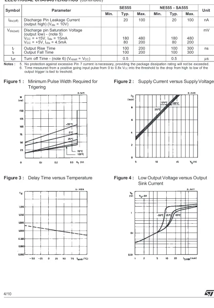
[image:58.612.82.521.105.737.2]Figure 1 : Minimum Pulse Width Required for Trigering
Figure 2 : Supply Current versus Supply Voltage
Figure 3 : Delay Time versus Temperature Figure 4 : Low Output Voltage versus Output Sink Current
NE555/SA555/SE555
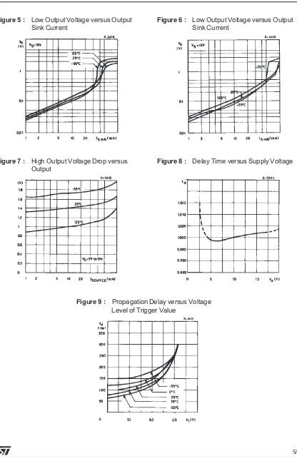
[image:58.612.346.491.295.442.2]Figure 5 : Low Output Voltage versus Output Sink Current
Figure 6 : Low Output Voltage versus Output Sink Current
[image:59.612.96.512.75.728.2]Figure 7 : High Output Voltage Drop versus Output
Figure 8 : Delay Time versus Supply Voltage
Figure 9 : Propagation Delay versus Voltage Level of Trigger Value
NE555/SA555/SE555
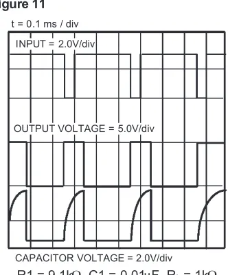
CAPACITOR VOLTAGE = 2.0V/div t = 0.1 ms / div
INPUT = 2.0V/div
OUTPUT VOLTAGE = 5.0V/div
[image:60.612.323.489.100.300.2]R1 = 9.1kΩ, C1 = 0.01µF, R = 1kL Ω Figure 11
Reset
Trigger
Output
R1
C1
Control Voltage
0.01µF
NE555
= 5 to 15V VCC
4 2
3 1
5 6 7 8 Figure 10
C (µF)
10
1.0
0.1
0.01
0.001
10µs 100µs 1.0 10 100 10 (t )d
ms ms ms s
10M
Ω
1MΩ
100k
Ω
10k
Ω
R1=
1kΩ
Figure 12 APPLICATION INFORMATION
MONOSTABLE OPERATION
In the monostable mode, the timer functions as a one-shot. Referring to figure 10 the external capaci-tor is initially held discharged by a transiscapaci-tor inside the timer.
The circuit triggers on a negative-going input signal when the level reaches 1/3 Vcc. Once triggered, the circuit remains in this state until the set time has elapsed, even if it is triggered again during this in-terval.The duration of the output HIGH stateis given by t = 1.1 R1C1and is easily determined by figure 12.
Notice that since the charge rate and the threshold level of the comparator are both directly proportional to supply voltage, the timing interval is independent of supply. Applying a negativepulse simultaneously to the reset terminal (pin 4) and the trigger terminal (pin 2) during the timing cycle discharges the exter-nal capacitor and causes the cycle to start over. The timing cycle now starts on the positive edge of the reset pulse. During the time the reset pulse in ap-plied, the output is driven to its LOW state. When a negativetrigger pulse is applied to pin 2, the flip-flop is set, releasing the short circuit across the external capacitor and driving the output HIGH. The voltage across the capacitor increases exponen-tially with the time constantτ= R1C1. When the volt-age across the capacitor equals 2/3 Vcc, the compa-rator resets the flip-flop which then discharge the ca-pacitor rapidly and drivers the output to its LOW state.
Figure 11 shows the actual waveforms generatedin this mode of operation.
When Reset is not used, it should be tied high to avoid any possibly or false triggering.
ASTABLE OPERATION
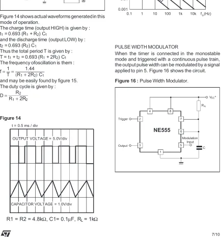
When the circuit is connected as shown in figure 13 (pin 2 and 6 connected)it triggers itself and free runs as a multivibrator. The external capacitor charges through R1and R2and discharges through R2only. Thus the duty cycle may be precisely set by the ratio of these two resistors.
In the astable mode of operation, C1charges and discharges between 1/3 Vccand 2/3 Vcc. As in the triggeredmode, the charge and discharge times and therefore frequency are independent of the supply voltage.
NE555/SA555/SE555