Dopant-induced random telegraph signal in nanoscale lateral silicon pn
diodes at low temperatures
Sri Purwiyanti, Roland Nowak, Daniel Moraru, Takeshi Mizuno, Djoko Hartanto et al.
Citation: Appl. Phys. Lett. 103, 243102 (2013); doi: 10.1063/1.4841735 View online: http://dx.doi.org/10.1063/1.4841735
View Table of Contents: http://apl.aip.org/resource/1/APPLAB/v103/i24
Published by the AIP Publishing LLC.
Additional information on Appl. Phys. Lett.
Journal Homepage: http://apl.aip.org/
Journal Information: http://apl.aip.org/about/about_the_journal
Top downloads: http://apl.aip.org/features/most_downloaded
Dopant-induced random telegraph signal in nanoscale lateral silicon
pn
diodes at low temperatures
Sri Purwiyanti,1,2Roland Nowak,1,3Daniel Moraru,1Takeshi Mizuno,1Djoko Hartanto,2 Ryszard Jablonski,3and Michiharu Tabe1,a)
1
Research Institute of Electronics, Shizuoka University, 3-5-1 Johoku, Naka-ku, Hamamatsu 432-8011, Japan 2
Department of Electrical Engineering, University of Indonesia, Depok, 16424 Jakarta, Indonesia 3
Division of Sensors and Measuring Systems, Warsaw University of Technology, Sw. A. Boboli 8, 02-525 Warsaw, Poland
(Received 21 September 2013; accepted 20 November 2013; published online 9 December 2013)
We studied current-voltage characteristics of nanoscalepndiodes having the junction formed in a laterally patterned ultrathin silicon-on-insulator layer. At temperatures below 30 K, we observed random telegraph signal (RTS) in a range of forward bias. Since RTS is observed only forpn
diodes, but not forpin diodes, one dopant among phosphorus donors or boron acceptors facing across the junction is likely responsible for potential changes affecting the current. Based also on potential measurements by low-temperature Kelvin probe force microscope, RTS is ascribed to trapping/detrapping of carriers by/from a single dopant near the farther edge of the depletion region.VC 2013 AIP Publishing LLC. [http://dx.doi.org/10.1063/1.4841735]
Nanoscale pn diodes have significant advantages over conventional diodes because of their low-dimensional poten-tial profiles and unique structural properties. Recently, a va-riety of topics related to downsized pn diodes have been extensively studied, i.e., interband tunneling in vertical and lateral Si nanodiodes,1,2 nanoscale avalanche photodiodes,3 radialpnjunction nanorods for solar cell applications,4and fundamental properties of two-dimensional pn junctions.5,6 However, there is another important aspect in doped nano-scale devices. With miniaturization of Si devices, the number of dopants is also reduced, and one or a few dopants may strongly affect the electrical characteristics of the devices. In fact, it is reported that in metal-oxide-semiconductor field-effect transistors (MOSFETs), single dopant atoms (donor or acceptor) in the channel determine the device characteristics.7–9 In contrast, effects of discrete dopants have not been reported inpndiodes, except for a report on photo-induced fluctuations of diode current.10
By further reduction in size ofpndiodes, however, the dis-creteness of dopants will undoubtedly gain an even more signif-icant role in the diode characteristics. In this work, our purpose is to identify signatures of individual dopants in the current-voltage (I-V) characteristics of nanoscale Sipnandpindiodes at different temperatures, in the dark condition. As a result, we observe random telegraph signal (RTS) at low temperatures, only for pndiodes. Based on this fact and supporting results obtained by Kelvin probe force microscopy (KFM), the RTS is ascribed to trapping/detrapping of a charge carrier by/from a single dopant atom in the depletion region of thepnjunction.
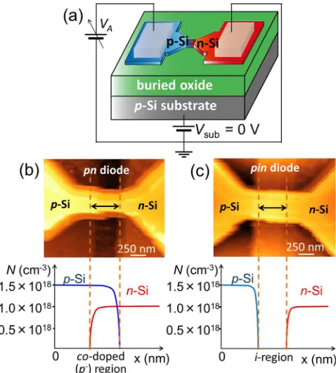
We fabricated, on a silicon-on-insulator (SOI) wafer, lateralpndiodes consisting of apnjunction, defined in a nar-row and thin Si region, coupled to fan-shaped leads (p- and
n-Si) and square-shaped pads, with Al contact electrodes, as shown in Fig.1(a). As reference devices, we also fabricated on the same sample pin diodes containing a nominally
intrinsic (i) layer between then- andp-pads. Electrical char-acteristics of thepnandpindiodes were measured by apply-ing a variable voltage to thep-region, with then-region and
p-Si substrate usually grounded. Figures1(b)and1(c)show atomic force microscope (AFM) images of pn and pin
diodes, respectively, including the junctions. For both types of diodes, the Si layer thickness is only5 nm, the length of the straight-patterned central region is about 1000 nm, and the width is 200 nm. The buried oxide layer is 150-nm-thick, and a 10-nm-thick SiO2layer was thermally grown for passivation, before defining Al contacts for thepandnleads.
FIG. 1. (a) Device structure of apndiode and measurement setup. (b), (c) AFM images and doping concentration profiles forpnjunctions (containing a co-doped region) andpinjunctions (containing an intrinsic region). a)Author to whom correspondence should be addressed. Electronic mail:
romtabe@rie.shizuoka.ac.jp
A conventional doping technique, based on thermal diffu-sion from a spin-coated silicate glass as a dopant source, was used to create phosphorus (P)-doped and boron (B)-doped regions. The lower panels in Figs. 1(b) and 1(c) show expected dopant concentration profiles across thepnandpin
diodes, respectively. P and B concentrations away from the junction are ND11018cm3 and NA1.51018cm3, respectively, as estimated from secondary ion mass spectrom-etry (SIMS) for thicker (50 nm) reference samples. All of the
pn diodes contain a co-doped region, doped both with P donors and with B acceptors. Due to the higher concentration of B compared to that of P, the co-doped region is effectively
p-type, and, therefore, the location of thepnjunction is at the boundary between the co-doped region and then-Si region. In thepindiodes, thei-region (nominally undoped) is not ideally intrinsic because the commercial SOI wafers have a native low doping with B (NA11015cm3). However, since the estimated number of B atoms in thei-region is one or less, it is reasonable to assume this region as intrinsic.
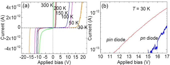
First, we measured the I-V characteristics of pndiodes to confirm their general behavior at different temperatures. Figure2(a)shows that, even in these ultrathin-Si diodes, rec-tifying behavior is observed in a wide temperature (T) range, between 300 and 30 K. With decreasing temperature, it is also seen that the voltage for the onset of forward current increases. This is caused by a reduction of the effective car-rier concentration due to dopant freeze-out effect,11,12which leads to an increase in the parasitic resistance of the leads. Therefore, at lower temperatures, because a significant amount of the externally applied voltage is consumed in the lead regions, the voltage drop across the pn junction is far below the applied voltage. A larger shift of onset-voltages between 150 and 100 K, as seen in Fig. 2(a), is consistent with the fact that the dopant freeze-out effect becomes prom-inent in this temperature range.11
In Fig. 2(b), we compare I-V curves measured at low temperatures (T¼30 K) for pn and pin diodes with nomi-nally same designed dimensions. However, due to enhanced oxidation rate of the co-doped region for thepndiodes, their cross-sectional area is significantly smaller than for thepin
diodes. Consequently, current is higher for thepindiodes. In the present experiment, 9pn diodes and 9pin diodes were measured in the low-temperature range (T¼6–30 K). Discrete current fluctuations can be found only for the pn
diodes (for 3 different devices), but for none of the pin
diodes. In thepindiodes, electron flux flowing from then-Si region to the i-Si region recombines within the i-region
with the hole flux flowing from the opposite direction. This is the major component of the total current, and the electron flux cannot usually reach the boundary of thep-type region without recombination inside the long i-region. In such pin diode structure, dopants are practically absent in the i-region and, therefore, potential barriers for electrons and holes are not expected to fluctuate in time. This different behavior of pn and pin diodes suggests that dopants, mixed inside the depletion region of apndiode, are most likely the origin of the current fluctuations. This will be further confirmed by KFM, as shown in the latter part of this paper.
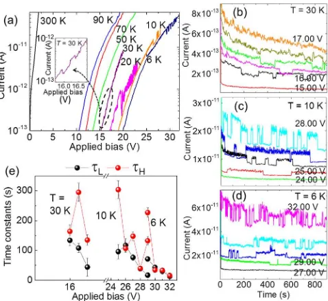
Since the effect of individual dopants is expected to become more prominent at low temperatures, we studied the
I-Vcurves mainly forT<100 K, as shown in Fig.3(a). It is found that noise becomes visible in theI-Vcharacteristics in a limited bias range, indeed only for low temperatures, below 30 K (as shown in the inset). In Figs.3(b)–3(d),I-time traces are shown for different temperatures, 30, 10, and 6 K, respec-tively. Applied bias was used as a parameter. For larger applied biases, a drift of the current in time is ascribed to the slow inversion of thep-Si layer, due to the low rate of minor-ity carrier generation at these low temperatures. It can be seen that, depending on bias, different behaviors can be found for the current noise. For low biases, the current can be treated as noise-free because the fluctuations have small amplitude (comparable with the noise level, 10 fA). In a certain bias range, RTS with two discrete current levels is clearly observed. RTS is, in general, associated with charge-state fluctuation of an oxide trap, as reported in a number of important papers on RTS in MOSFETs.13–16In these studies, it is usual to extract the properties of the trap from the gate voltage dependence of the RTS. However, in pn diodes, a gate is not available. An analysis of the RTS as a function of temperature and bias applied across thepnjunction is shown next.
Time constants for low (sL) and high (sH) current levels, extracted from the I-time data, are shown in Fig.3(e) as a function of applied forward bias. It can be seen that bothsL andsHdepend on applied bias, despite the larger scattering for the sHdata. According to the fundamental theory of the Shockley-Read-Hall (SRH) statistics,17 applied to noise in
pn junctions,18 such dependencies indicate that the RTS is due to a generation-recombination center. At the low temper-atures of our measurements, due to the strong freeze-out effect, such a center responsible for RTS is likely a dopant located in the depletion region. In fact, the values of the time
FIG. 2. (a) Temperature dependence of
I-Vcharacteristics for apndiode under reverse and forward bias. (b)I-V char-acteristics of a pn diode and a pin
diode at low temperature (T¼30 K) under forward bias.
constants are consistent with the carrier dwell time in typical shallow dopant atoms, such as P or B, in Si (longer than 10 s at T<30 K).12 The lack of observation of the noise for
T>30 K may be due to the fact that the dwell time in dop-ants becomes shorter than the time resolution of our meas-urements and the charge state switching cannot be detected. For higher biases, the current starts to fluctuate between three or more levels, with a significantly more complex behavior, suggesting that not only one, but several charge traps are involved.
As indicated above, RTS is likely due to trapping/detrap-ping of a charge carrier (electron or hole) by/from a single dopant atom. Figures4(a) and4(b) illustrate the band dia-grams for a forward-biaspndiode. For nanoscalepndiodes, we combined the theory for bulkpnjunctions with individual dopant potentials in the depletion region, as schematically illustrated in the diagrams. For simplicity, we consider only electron diffusion current under forward bias condition (It is noted that a symmetrical argument holds for hole current). Although there are a number of dopants in the entire deple-tion region, the most critical dopant that affects the electron current is only one B atom located near the farther edge (on thep-Si side) of the depletion region. This edge of the deple-tion region is defined as a “sensitive region,” as explained in more details later, because the potential here works as a bar-rier for electrons and limits electron flux entering into thep -Si region. While the B dopant remains neutral, B0 (with a hole captured), a high electron current can flow [Fig.4(a)]. However, when the B dopant is ionized, B
(by capturing an electron), the local electronic potential is raised, and the elec-tron current is suppressed to the lower level [Fig.4(b)].
Next, we evaluate the number of dopants located in this “sensitive region,” critically affecting the current. First, the depletion region width (Wd) is calculated based on
conventionalpnjunction theory, forT¼30 K.11This is plot-ted in Fig. 4(d) as a function of the potential difference between the p and n regions (DVpn). In the absence of applied bias (VA¼0 V), as marked on the right, Wd is approximately 50 nm. Then, we quantitatively define a “sensitive region” considering the effect of individual dop-ants inside the depletion region. The sensitive region extends from the left boundary of the depletion region to the right, covering a potential difference of 45 meV. This value basi-cally corresponds to the charging energy of a B acceptor in Si.19The width of this sensitive region (Ws) is also plotted in Fig.4(d). This allows us to evaluate the number of B dopants present inside Ws, as shown in Fig.4(e). The dopant concen-tration at the depletion region’s boundary is assumed to lie in the range of 0.51018–1.51018cm3
since the exact value of dopant concentration cannot be directly measured for such an ultrathin Si film. The lowest B concentration (0.51018cm3
) is, basically, consistent with our experi-mental data. As indicated on the graph, depending on the number of B dopants found inWs, three distinct regimes can be identified for this lowest concentration of B. In regime I, no B dopants are included in Ws; accordingly, RTS is not expected. In regime II, the number of B dopants in Ws is around one. This corresponds to the bias range for the obser-vation of the two-level RTS. For regime III, two or more B dopants are incorporated inWs, resulting in a multiple-level RTS. Thus, this evaluation of the number of critical dopants confirms that the RTS characteristics can be reasonably ascribed to B dopants located nearby the boundary of the depletion region.
For directly observing the potential landscape in nano-scale pn junctions, we carried out KFM measurements, as FIG. 3. (a)I-Vcharacteristics for apndiode in forward bias atT<100 K
(data for 300 K is shown as reference). At low temperatures,I-V measure-ments were stopped at biases not far beyond the bias for noise observation. Inset shows RTS-like features in the data forT¼30 K. (b), (d)I-time traces as a function of applied bias for 30 K (0.25 V step), 10 K (1.0 V step), and, respectively, 6 K (1.0 V step). (e) Time constants, extracted from theI-time data for low (sL) and high (sH) current levels, as a function of applied bias.
FIG. 4. (a) and (b) Band diagrams of pndiodes under forward bias. The band diagrams are drawn based on bulkpnjunction theory, combined with individual dopant potentials in the depletion region. One B acceptor in dif-ferent charge states, neutral (B0) and, respectively, ionized (B), affects the
described in more details in Ref.20. Here, in Fig. 5(a), we show a result measured at low temperature (T¼15 K) for a
pndiode, at zero applied bias. A region containing prominent potential fluctuations can be observed between flat-potential areas. We previously demonstrated, based on the applied bias dependence,20that this region corresponds to the deple-tion region of thepndiode. Figure5(b)shows a line profile across the depletion region, in order to illustrate the potential fluctuations localized to the depletion region. Since KFM is a scanning-probe technique, the measurement can be charac-terized not only as a function of distance but also as a func-tion of time. In Fig.5(b), scan distance was converted into scan time by knowing the measurement time per point. In this line profile, time-dependent potential fluctuations can be seen as random fluctuations between several levels. Such time-dependent fluctuations can be ascribed to the fluctua-tions of the charge states of dopants under the electric field formed in the depletion region. Since a number of dopants contribute to this potential, the fluctuations do not occur only between two distinct levels. However, undulations on a scale of 10 nm are observed at the boundary of the depletion region. These features are consistent with individual dopant potentials (some B acceptors are illustrated in Fig. 5(a)), strongly affecting the boundary of the depletion region.
The KFM results presented here suggest the significant impact of individual dopants in the depletion region, in par-ticular at its boundaries, on the potential landscape of nano-scalepndiodes. These findings are basically consistent with
our model of a dopant in the depletion region being responsi-ble for the observation of RTS in theI-Vcharacteristics.
In conclusion, we fabricated nanoscale ultrathin lateral
pnjunctions and studied their behavior by electrical charac-terization and potential measurements. We observed currents fluctuations as RTS under forward bias at low temperatures. The RTS is due to potential fluctuations caused by trapping and detrapping of charge carriers by/from individual dopants in the depletion region. KFM images, exhibiting time-dependent potential fluctuations in the depletion region, as well as local modulations of the junction’s boundaries, sup-port our model. These results provide further evidence about the enhanced importance of discrete, individual dopants in the transport mechanism of nanoscalepndiodes.
We thank S. Miki and M. Kobayashi for their support in device fabrication and A. Udhiarto for useful discussions. This work was partially supported by Grants-in-Aid for sci-entific research (MEXT/JSPS KAKENHI 23226009, 25630144, and 22310085).
1
H. Schmid, C. Bessire, M. T. Bjork, A. Schenk, and H. Riel,Nano Lett. 12, 699 (2012).
2C. Aydin, A. Zaslavsky, S. Luryi, S. Cristoloveanu, D. Mariolle,
D. Fraboulet, and S. Deleonibus,Appl. Phys. Lett.84, 1780 (2004). 3
O. Hayden, R. Agarwal, and C. M. Lieber,Nature5, 352 (2006).
4
B. M. Kayes, H. A. Atwater, and N. S. Lewis,J. Appl. Phys.97, 114302
(2005).
5S. Petrosyan, A. Yesayan, D. Reuter, and A. D. Wieck,Appl. Phys. Lett.
84, 3313 (2004).
6
D. Reuter, C. Werner, A. D. Wieck, and S. Petrosyan,Appl. Phys. Lett. 86, 162110 (2005).
7H. Sellier, G. P. Lansbergen, J. Caro, N. Collaert, I. Ferain, M. Jurczak, S.
Biesemans, and S. Rogge,Phys. Rev. Lett.97, 206805 (2006).
8
M. Tabe, D. Moraru, M. Ligowski, M. Anwar, R. Jablonski, Y. Ono, and T. Mizuno,Phys. Rev. Lett.105, 016803 (2010).
9Y. Ono, K. Nishiguchi, A. Fujiwara, H. Inokawa, and Y. Takahashi,Appl.
Phys. Lett.90, 102106 (2007).
10
A. Udhiarto, D. Moraru, S. Purwiyanti, T. Mizuno, and M. Tabe, Appl. Phys. Express5, 112201 (2012).
11S. M. Sze,Physics of Semiconductor Devices, 3rd ed. (Wiley, New Jersey, 2007).
12
D. Foty,Cryogenics30, 1056 (1990).
13R. K. Ralls, W. J. Skocpol, L. D. Jackel, R. E. Howard, L. A. Fetter, R. W.
Epworth, and D. M. Tennant,Phys. Rev. Lett.52, 228 (1984). 14
N. V. Amarasinghe, Z. Celik-Butler, and A. Keshavarz,J. Appl. Phys.89,
5526 (2001).
15J.-W. Lee, H. Shin, and J.-H. Lee,Appl. Phys. Lett.96, 043502 (2010). 16Y. Mori, H. Yoshimata, K. Takeda, and R. Yamada,J. Appl. Phys.111,
104513 (2012). 17
W. Shockley and W. T. Read, Jr.,Phys. Rev.87, 835 (1952).
18S. T. Hsu, R. J. Whittier, and C. A. Mead,Solid-State Electron.13, 1055
(1970). 19
A. K. Ramdas and S. Rodriguez,Rep. Prog. Phys.44, 1297 (1981).
20
R. Nowak, D. Moraru, T. Mizuno, R. Jablonski, and M. Tabe,Appl. Phys. Lett.102, 083109 (2013).
FIG. 5. (a) Electronic potential landscape measured by low-temperature (T¼15 K) KFM across a pn junction’s depletion region. The depletion region is delineated by white dashed boundaries. B dopants are schemati-cally shown at the boundary. (b) Line profile illustrating potential fluctua-tions as a function of both scan distance and scan time.