DENOISING ALGORITHM FOR THE PIXEL-RESPONSE NON-UNIFORMITY
CORRECTION OF A SCIENTIFIC CMOS UNDER LOW LIGHT CONDITIONS
Changmiao Hu a, Yang Bai a, *, Ping Tang a a
Institute of Remote Sensing and Digital Earth, Chinese Academy of Sciences, Beijing 100101, P. R. China (hucm, baiyang, tangping)@radi.ac.cn
Commission III, WG III/5
KEY WORDS: CMOS, Denoising algorithm, Pixel-response non-uniformity
ABSTRACT:
We present a denoising algorithm for the pixel-response non-uniformity correction of a scientific complementary metal–oxide– semiconductor (CMOS) image sensor, which captures images under extremely low-light conditions. By analyzing the integrating sphere experimental data, we present a pixel-by-pixel flat-field denoising algorithm to remove this fixed pattern noise, which occur in low-light conditions and high pixel response readouts. The response of the CMOS image sensor imaging system to the uniform radiance field shows a high level of spatial uniformity after the denoising algorithm has been applied.
* Corresponding author
1. INTRODUCTION
Complementary metal–oxide–semiconductor (CMOS) image sensors are the most extensively used sensor devices in generic digital cameras because of their high resolution, acceptable linearity, small size, cheap price, rapid response, and durability (Fowler, 2009). In spite of these characteristics, CMOS image sensors are imperfect detectors when they are used as instruments for generic scientific imaging. For CMOS, obtaining accurate radiometric measurements is difficult and the signal-to-noise ratio (SNR) is always unstable. Several noise sources, such as dark current noise, amplifier noise, read noise, and fixed pattern noise, which are inherent in the performance of a camera, alter the digital number (DN) value of each pixel and degrade real image quality (Kawai, 2004; Kim, 2009; Zhang, 2011). The noise sources of charge-coupled device (CCD) cameras and their nature have been extensively investigated and analyzed (Eastman, 2001; Haralabidis, 2005). In this study, we focus on CMOS image denoising under extremely low-light conditions. We use an integrating sphere to obtain experimental data and generic CCD camera noise analysis techniques to remove noise. We detect fixed pattern noise, which is inherent in the performance of CMOS and occurs in low-light conditions and high pixel response readouts. We present a pixel-by-pixel flat-field denoising algorithm to remove this fixed pattern noise.
2. MATERIAL AND METHOD 2.1 Scientific CMOS Image Sensor
We use the Fairchild Imaging CIS2521F scientific CMOS (sCMOS) image sensor in this study. The CIS2521F has high frames per second (fps) imaging rates and high sensitivity, which are important for Unmanned Vehicle Systems (UVS) imaging under extremely low-light conditions in remote sensing mapping applications.
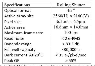
The Fairchild Imaging CIS2521F is a large-format, low-noise sCMOS image sensor intended for applications requiring high-quality imaging under extremely low-light conditions (Fairchild Imaging, 2015). The device features an array of five-transistor pixels on a 6.5 µm pitch with an active imaging area of 2,560 (H) × 2,160 (V) pixels. The CIS2521F delivers extreme low-light sensitivity with read noise less than 2e-RMS in rolling shutter, read noise less than 5e-RMS in global shutter, and quantum efficiency greater than 55%. The sensor runs in rolling and global shutter readout modes. The sensor has two analog-to-digital converter channels per column, with one optimized for low light levels and the other optimized for high light levels, enabling high dynamic range data collection in a single image. These features, combined with 5.5 megapixel resolution and 100 fps imaging rates, make the CIS2521F an imaging device ideally suited for a variety of low-light-level camera applications (see Table 1 and Figure 1).
2.2 Experimental Procedures
For aerial remote sensing, including the UVS platform, the CMOS image has two distinct pixel-response non-uniformity characteristics under extremely low-light conditions compared with images under normal ambient light conditions. First, the CMOS pixel response noise level increases with the increase in sensitivity. Similarly, the noise of the CMOS image captured by a general digital camera increases with the increase in the ISO value to a high level. Second, several local regions are overexposed, which is caused by several bright light sources in low-light conditions. The local overexposed area not only affects the entire gray-scale uniformity of the remote sensing image but also easily induces amplified noise. Figure 2 is a partial CIS2521F CMOS image, which is captured in a 10 lux low-light environment. In this image, the noise is obvious and the overexposed regions are observed between the street light (point A) and bright windows (point B).
In this study, we combine traditional non-uniformity correction based on the integrating sphere experimental data and NL-Bayes image denoising algorithm to improve the CMOS image quality under extremely low-light conditions.
Specifications Rolling Shutter
Optical format 4/3”
Active array size 2560(H) × 2160(V)
Pixel size 6.5μm × 6.5μm
Active area 16.6mm × 14.0mm
Maximum frame rate 100 fps
Read noise < 2 e-RMS
Dynamic range > 83.5 dB
Full well capacity > 30,000
e-Dark current At 20°C < 35 e-/pixel/sec
Peak QE > 55%
Table 1. CIS2521F Specifications (Fairchild Imaging, 2015)
Figure 1. Block diagram of CIS2521F (Fairchild Imaging, 2015)
Figure 2. CMOS imaging under extremely low light conditions, 10 lux, 500 × 500 pixels
Different from the traditional absolute radiometric calibration based on the integrating sphere experimental data, we use an integrating sphere not to determine the quantitative relationship of each pixel between incoming radiance and final output DN value. We analyze the output DN value only and focus on the factors that lead to pixel non-uniformity. Pixel non-uniformity mainly accounts for the lower quantitative level of CMOS than CCD, and the noise is always obvious under extremely low-light conditions.
The laboratory equipment includes an integrating sphere, the computer includes an image collection card, and the camera includes CIS2521F CMOS, as shown in Figure 3.
integrating sphere
camera CMOS:CIS2521F
computer Image collection card
Figure 3. Process of different flat-field image collection using integrating sphere
Based on the experimental results of the studies of Ren and Ralf (Ren, 2007; Ralf, 2010), the response function of each pixel can be expressed in Eq. (1):
N
NDN
A
A
L
A
L
A
L
V
2
2 1
0 (1)
where VDN = CMOS pixels output DN value A0= dark current noise
A1,A2,…,AN= radiation correction coefficients
L = radiance of band at center wavelength of
The radiometric calibration procedure is employed to select ngroup incoming radiance, which is composed of n groups measured by using Eq. (1). VDN-i (i=1, 2, …, n) denotes the
known image output DN value, Li (i=1, 2, …, n) denotes the
incoming radiance, and A0 denotes the dark current noise. When
n > N, the radiation correction coefficient Ai (i=1, 2, …, n) can be solved (Wang, 2010). We do not consider the absolute radiometric calibration and only focus on the noise analysis of
A0 and VDN−A0. Thus, we only focus on the final CMOS output DN value and do not consider the absolute incoming radiance value of the integrating sphere. The illuminometer is not used, and the mean values of VDN-i (i=1, 2, …, n) are only counted.
Dark current noise is a main factor that leads to pixel response non-uniformity for CCD, but has no effect on the input radiance. Therefore, dark current noise can be detected under no light conditions and can be isolated from other noise factors by VDN
− A0.
By non-uniformity detection and analysis of VDN −A0 at the same gain setting and the same integration time, we derive 10 group output DN values at 10 different group radiances using an integrating sphere and subtract the corresponding dark current noise.
The quality of the pixel-response non-uniformity correction performance was quantified by using Eq. (2) (Marta, 2007), and we refer to it as the non-uniformity percentage (NU):
where VNU= non-uniformity percentage of a image
VAvg= average value of all the M x N image’s pixels Vij = the pixel DN value at (i, j)
We obtain two images under the same imaging conditions to analyze the CMOS noise situation and detect system noise at the same gain setting, the same integration time, and the same integrating sphere illumination. For these two images, we calculate the correlation coefficient by using Eq. (3):
= correlation coefficient between image X and Y Cov(X, Y) = covariance of image X and Y
D(X), D(Y) = image X’s variance, image Y’s variance An intuitive way evaluate the correlation of the two images is overlay display in a remote sensing software window. We use the ENVI software to open two images in two display windows and link the displays (ENVI 4.7, 2009). In the zoom window, the strength of the correlation can be intuitively observed by clicking the mouse interactive display on the same zoomed area of the two images. Figure 4 is a correlation analysis example using the zoom window of ENVI. A, B, C, and D are four parts of four flat-field data collected by the integrating sphere at different imaging conditions, and the correlation coefficients are
AB
= 0.402867 and CD = 0.9269770. In Figure 4, we observed certain similarities between C and D, but hardly recognized a connection between A and B.
Figure 4. Correlation analysis, A, B, C, and D are a part of four flat-field images, displayed in ENVI’s zoom window, 20 × 20 pixels, AB = 0.402867,
CD
= 0.9269770
We assume that a fixed pattern noise may exist if several correlations are observed in two images in an imaging condition. We obtain 10 images in this imaging condition and calculate the
mean image of the 10 images to separate the fixed pattern noise from the flat-field images. The mean image can be used as denoising reference image in this imaging condition. V(φ) is the mean image and φ is the integrating sphere illumination. We
matrix can be used to correct the pixel non-uniformity imaging around the illumination φ.
Eq. (3) can only be used to correct the images under one approximate imaging condition. We used the pixel-by-pixel linear correction method based on the research of Bellia (Bellia, 2003) to expand the scope of pixel non-uniformity correction. At the same gain setting and integration time, for 10 different levels of illumination imaging, if fixed pattern noise was observed in the two adjacent illuminations φ1 and φ2, then we repeat the previous experiment, obtain 10 images in the corresponding integrating sphere illumination, and calculate the corresponding mean images V(φ1) and V(φ2). As a result, we
By using Eqs. (7) and (8) for each CMOS pixel, we can derive the gain and offset matrices. These matrices can be used to correct the pixel non-uniformity imaging between the illuminations φ1 and φ2. This correction process is conducted pixel by pixel.
By repeating the integrating sphere experiment, we obtain the gain and offset matrices at different imaging conditions and establish the non-uniformity correction for specific fixed pattern noise of CMOS.
For the actual acquired image, which was captured under extremely low-light conditions by CIS2521F CMOS as the
payload of a UVS, we generated a lookup table (LUT) to derive the corresponding gain and offset matrices. Notably, remote sensing images under low-light conditions may have several local highlighted areas, which affect the determination of the LUT baseline. We use histogram statistics and automatic threshold to divide different illumination areas simply.
3. RESULTS
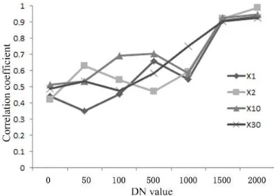
In this study, the CMOS has four gain settings (×1, ×2, ×10, ×30). We set six group integration times for the integrating sphere experiment (1, 100, 200, 600, 1250, 2400, in microseconds). We do not consider the absolute calibration, only the relative denoising. The sphere experiment does not consider the radiation illuminance and lens aperture settings. We use the output average DN value of flat-field images at four gain settings and different integration times as a grouped foundation and analyze the noise correlation of each image group, as shown in Figure 5. We determined that, at the average DN values of 1,500 and 2,000, all the correlation coefficients of the four gain settings of flat-field images are more than 0.9. As such, fixed pattern system noise may exist.
Figure 5. Correlation coefficient with the DN value
Taking the flat-field images with 1,500 average DN value, ×10 gain, and 1 and 2,500 ms integration times as an example, the correlation analysis showed that the correlation coefficients of images at two integration times are more than 0.9. This finding shows that the integration time will not affect the noise situation. By conducting pixel response non-uniformity correction using Eq. (4), the average UN value decreases from 4.4% to 2.4%, as shown in Table 2. This finding indicates the presence of fixed pattern system noise that can be effectively removed. The same treatment is effective for flat-field images with 2,000 average DN value and ×10 gain. The pixel response non-uniformity correction model at ×10 gain can be obtained by determining the mean value of the images at 1,500 and 2,000 DN using Eqs. (5) and (6). Similarly, we calculate the correction model at ×1, ×2, and ×30 gains to achieve the removal of this kind of system noise.
The correction effect analysis of the fixed pattern system noise is shown in Figure 6. Figure 6A is a partial 400 × 400 pixel image before correction, and Figure 6B is a partial image after correction. The pixel-response non-uniformity situation before and after correction is shown in Figures 6C and 6D. The results show that the non-uniformity has been significantly improved. Figure 6A shows that the existence of apparent vertical stripe noise. Figure 6B shows that the vertical stripe no longer exist
after correction. We determine that this vertical stripe noise is mainly composed of fixed pattern system noise. Based on the CMOS device imaging process shown in Figure 1, we infer that this noise may be generated by the column amplifiers as the vertical output. Noise in Figure 6B is mainly composed of random noise and dark current horizontal stripes. The noise intensity shown in Figure 6B corresponds to that shown in Figure 6D. After correction, the noise level is still high, which may cause high noise in the actual image.
Number Gain_Time_No
DN value
UN
before after
×10_T1_01 1496.99 4.45597% 2.50655%
×10_T1_02 1499.08 4.43398% 2.39437%
×10_T1_03 1498.16 4.3828% 2.3167%
×10_T1_04 1498.86 4.41573% 2.3583% ×10_T1_05 1493.25 4.45282% 2.54576%
×10_T1_06 1496.03 4.46271% 2.5561%
×10_T1_07 1494.15 4.43751% 2.54736%
×10_T1_08 1492.9 4.45987% 2.56833%
×10_T2500_01 1495.34 4.4157% 2.48597%
×10_T2500_02 1497 4.40326% 2.42657%
×10_T2500_03 1498.73 4.3679% 2.27021% ×10_T2500_04 1500.43 4.4266% 2.34869% ×10_T2500_05 1497.79 4.3824% 2.35423% Table 2: Non-uniformity measure of CMOS imaging in the various integrating sphere output radiance conditions
A
B
C
D
Figure 6. Pixel-response non-uniformity correction for fixed pattern system noise, A: Original image, 400 × 400 pixels, average DN value 1496; B: Correction result image; C&D: corresponds to A&B’s 3D display
4. CONCLUSIONS
In this study, we presented a denoising algorithm for the pixel-response non-uniformity correction of the CIS2521F sCMOS image sensor utilized under extremely low-light conditions and the experimental method designed for its implementation. After the output pixel response exceeds a certain value, the CMOS exhibits a fixed pattern noise, which is expressed as regular vertical stripes, and has a strong correlation under the same imaging conditions. We estimate that this system noise is
mainly caused by the CMOS column amplifiers. Our pixel-by-pixel non-uniformity correction can effectively eliminate this noise. The denoising effect is good for the local highlighted region of the aerial remote sensing image imaging under low-light conditions.
ACKNOWLEDGEMENTS
This work was supported by the National High Technology Research and Development Program (863) under Grant 2013AA12A301.
REFERENCES
Fowler B. et al., 2009. Wide dynamic range low light level CMOS image sensor, in Proc. Int. Image Sensor Workshop, Bergen, Norway, Jun. pp. 1–4.
Kawai N. and Kawahito S., 2004. Noise analysis of high-gain, low-noise column readout circuits for CMOS image sensors, IEEE Trans. Electron Devices, vol. 51, no. 2, pp. 185–194, Feb. Kim B C, Jeon J, Shin H. 2009. Temporal Noise Analysis and Reduction Method in CMOS Image Sensor Readout Circuit. IEEE Transactions on Electron Devices. 56(11):2489-2495. Zhang Y. 2011. A Novel on-Chip Denoising Method for Temporal Noise of CMOS Image Sensor. Chinese Journal of Sensors & Actuators. 24(6):859-863.
Eastman Kodak Company. 2001. CCD Image Sensor Noise Sources, Application Note, Image Sensor Solutions. http://www.kodak.com/go/imagers.
Haralabidis P. E. and Pilinis C., 2005. Linear color camera model for a skylight colorimeter with emphasis on the imaging pipeline noise performance. J. Electron. Imaging 14, 043005 Fairchild Imaging, CIS2521, 2015, Megapixel Ultra Low Noise sCMOS Image Sensor, Fairchild Imaging,
http://www.fairchildimaging.com/catalog/focal-plane-arrays/scmos/cis2521
Ren Jianwei, Wan zhi, Li Xiansheng et al.., 2007. Radiarion transfer characteristic and calibrating method for space optical remote sensor. Optics and Precision Engineering. 15(8): 1186-1190
Ralf Widenhorn, Justin C. Dunlap, Erik Bodegom.2010. Exposure time dependence of dark current in CCD imagers. IEEE Trans. Electron Devices. 57(3): 581-587
Wang Wenhua, He Bin, Han Shuangli. 2010. Correction of nonuniformity in CCD imaging for remote sensing. 18(6): 1420-1428
Ralf Windenhorn, lnes Hartwig, Justin C. Dunlap et al.., 2009. Influence of illumination on dark current in charge-coupled device imagers. 18(3):033015
Marta D L, Jaume P, Montserrat A, et al. 2007. Optimized algorithm for the spatial nonuniformity correction of an imaging system based on a charge-coupled device color camera. Applied Optics, 46(2):167-174.
ENVI version 4.7, 2009. August, Edition Copyright © ITT Visual Information Solutions All Rights Reserved ENVI Reference Guide 20REF47DOC.
Bellia L., Cesarano A., Minichiello F., Sibilio S., and Spada G., 2003. Calibration procedures of a CCD camera for photometric Measurements. presented at IMTC 2003-Instrumentation and Measurement Technology Conference, Vail, Colo., 20–22