LM1577, LM2577
www.ti.com SNOS658D – JUNE 1999 – REVISED APRIL 2013
LM1577/LM2577 SIMPLE SWITCHER
®
Step-Up Voltage Regulator
Check for Samples: LM1577, LM2577
FEATURES DESCRIPTION
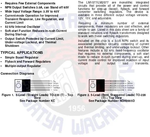
• Requires Few External Components• NPN Output Switches 3.0A, can Stand off 65V
The LM1577/LM2577 are monolithic integrated circuits that provide all of the power and control functions for step-up (boost), flyback, and forward • Wide Input Voltage Range: 3.5V to 40V converter switching regulators. The device is • Current-mode Operation for Improved
Transient Response, Line Regulation, and
available in three different output voltage versions: 12V, 15V, and adjustable.
Current Limit Requiring a minimum number of external
• 52 kHz Internal Oscillator
• Soft-start Function Reduces In-rush Current During Start-up
• Output Switch Protected by Current Limit, Under-voltage Lockout, and Thermal Shutdown
TYPICAL APPLICATIONS
• Simple Boost Regulator• Flyback and Forward Regulators
• Multiple-output Regulator
Connection Diagrams
components, these regulators are cost effective, and simple to use. Listed in this data sheet are a family of standard inductors and flyback transformers designed to work with these switching regulators.
Included on the chip is a 3.0A NPN switch and its associated protection circuitry, consisting of current and thermal limiting, and undervoltage lockout. Other features include a 52 kHz fixed-frequency oscillator that requires no external components, a soft start mode to reduce in-rush current during start-up, and current mode control for improved rejection of input voltage and output load transients.
Figure 1. 5-Lead (Straight Leads) TO-220 (T) – Top Figure 2. 5-Lead (Bent, Staggered Leads) TO-220 View (T) – Top View
LM1577, LM2577
LM1577, LM2577
SNOS658D – JUNE 1999 – REVISED APRIL 2013 www.ti.com
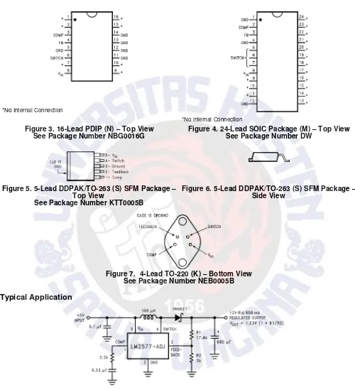
*No Internal Connection *No internal Connection
Figure 3. 16-Lead PDIP (N) – Top View Figure 4. 24-Lead SOIC Package (M) – Top View See Package Number NBG0016G See Package Number DW
Figure 5. 5-Lead DDPAK/TO-263 (S) SFM Package – Figure 6. 5-Lead DDPAK/TO-263 (S) SFM Package – Top View Side View
See Package Number KTT0005B
Figure 7. 4-Lead TO-220 (K) – Bottom View See Package Number NEB0005B
Typical Application
Note: Pin numbers shown are for TO-220 (T) package.
LM1577, LM2577
LM1577, LM2577
www.ti.com SNOS658D – JUNE 1999 – REVISED APRIL 2013
Absolute Maximum Ratings
(1) (2)Supply Voltage 45V
Output Switch Voltage 65V
Output Switch Current (3) 6.0A
Power Dissipation Internally Limited
Storage Temperature Range −65°C to +150°C
Lead Temperature Soldering, 10 sec. 260°C
Maximum Junction Temperature 150°C
Minimum ESD Rating C = 100 pF, R = 1.5 kΩ 2 kV
(1) Absolute Maximum Ratings indicate limits beyond which damage to the device may occur. Operating ratings indicate conditions the device is intended to be functional, but device parameter specifications may not be ensured under these conditions. For ensured specifications and test conditions, see the Electrical Characteristics.
(2) If Military/Aerospace specified devices are required, please contact the Texas Instruments Sales Office/ Distributors for availability and specifications.
(3) Due to timing considerations of the LM1577/LM2577 current limit circuit, output current cannot be internally limited when the LM1577/LM2577 is used as a step-up regulator. To prevent damage to the switch, its current must be externally limited to 6.0A. However, output current is internally limited when the LM1577/LM2577 is used as a flyback or forward converter regulator in accordance to the Application Hints.
Operating Ratings
Supply Voltage 3.5V ≤ VIN ≤ 40V
Output Switch Voltage 0V ≤ VSWITCH ≤ 60V
Output Switch Current ISWITCH ≤ 3.0A
Junction Temperature Range LM1577 −55°C ≤ TJ ≤ +150°C
LM1577, LM2577
LM1577, LM2577
www.ti.com SNOS658D – JUNE 1999 – REVISED APRIL 2013
Electrical Characteristics
—
LM1577-ADJ, LM2577-ADJ
Specifications with standard type face are for TJ = 25°C, and those in bold type face apply over full Operating Temperature
Range. Unless otherwise specified, VIN = 5V, VFEEDBACK = VREF, and ISWITCH = 0.
Symbol Parameter Conditions Typical LM1577-ADJ
Limit (1) (2) LM2577-ADJ Limit (3) (Limits)Units
SYSTEM PARAMETERS Circuit of Figure 31 (4)
VOUT Output Voltage VIN = 5V to 10V
ILOAD = 100 mA to 800 mA (1) 12.0 V
11.60/11.40 11.60/11.40 V(min) 12.40/12.60 12.40/12.60 V(max)
ΔVOUT/ΔVIN Line Regulation VIN = 3.5V to 10V ILOAD = 300 mA
20 mV
50/100 50/100 mV(max)
ΔVOUT/ΔILOA D
Load Regulation VIN = 5V
ILOAD = 100 mA to 800 mA
20 mV
50/100 50/100 mV(max)
Efficiency VIN = 5V, ILOAD = 800 mA 80 %
DEVICE PARAMETERS
IS Input Supply Current VFEEDBACK = 1.5V (Switch Off) 7.5 mA 10.0/14.0 10.0/14.0 mA(max)
ISWITCH = 2.0A
VCOMP = 2.0V (Max Duty Cycle)
25 mA
50/85 50/85 mA(max) VUV Input Supply
Undervoltage Lockout
ISWITCH = 100 mA 2.90 V
2.70/2.65 2.70/2.65 V(min) 3.10/3.15 3.10/3.15 V(max) fO Oscillator Frequency Measured at Switch Pin
ISWITCH = 100 mA
52 kHz
48/42 48/42 kHz(min) 56/62 56/62 kHz(max) VREF Reference
Voltage
Measured at Feedback Pin VIN = 3.5V to 40V VCOMP = 1.0V
V 1.230 1.214/1.206 1.214/1.206 V(min)
1.246/1.254 1.246/1.254 V(max)
ΔVREF/ΔVIN Reference Voltage Line Regulation
VIN = 3.5V to 40V 0.5 mV
IB Error Amp Input Bias Current
VCOMP = 1.0V 100 nA
300/800 300/800 nA(max) GM Error Amp
Transconductance
ICOMP = −30 μA to +30 μA VCOMP = 1.0V
3700 μmho
2400/1600 2400/1600 μmho(min)
4800/5800 4800/5800 μmho(max)
AVOL Error Amp Voltage Gain VCOMP = 1.1V to 1.9V RCOMP = 1.0 MΩ(5)
800 V/V
500/250 500/250 V/V(min) Error Amplifier
Output Swing
Upper Limit VFEEDBACK = 1.0V
2.4 V
2.2/2.0 2.2/2.0 V(min) Lower Limit
VFEEDBACK = 1.5V
0.3 V
0.40/0.55 0.40/0.55 V(max)
(1) All limits ensured at room temperature (standard type face) and at temperature extremes (boldface type). All limits are used to calculate Outgoing Quality Level, and are 100% production tested.
(2) A military RETS electrical test specification is available on request. At the time of printing, the LM1577K-12/883, LM1577K-15/883, and LM1577K-ADJ/883 RETS specifications complied fully with the boldface limits in these columns. The LM1577K-12/883, LM1577K- 15/883, and LM1577K-ADJ/883 may also be procured to Standard Military Drawing specifications.
(3) All limits ensured at room temperature (standard type face) and at temperature extremes (boldface type). All room temperature limits are 100% production tested. All limits at temperature extremes are ensured via correlation using standard Statistical Quality Control (SQC) methods.
LM1577, LM2577
LM1577, LM2577
LM1577, LM2577
LM1577, LM2577
SNOS658D – JUNE 1999 – REVISED APRIL 2013 www.ti.com
Electrical Characteristics
—
LM1577-ADJ, LM2577-ADJ (continued)
Specifications with standard type face are for TJ = 25°C, and those in bold type face apply over full Operating Temperature
Range. Unless otherwise specified, VIN = 5V, VFEEDBACK = VREF, and ISWITCH = 0.
Symbol Parameter Conditions Typical LM1577-ADJ
Limit (1) (2) LM2577-ADJ Limit (3) (Limits)Units Error Amp
Output Current
VFEEDBACK = 1.0V to 1.5V VCOMP = 1.0V
±200 μA
±130/±90 ±130/±90 μA(min)
±300/±400 ±300/±400 μA(max)
ISS Soft Start Current VFEEDBACK = 1.0V VCOMP = 0V
5.0 μA
2.5/1.5 2.5/1.5 μA(min)
7.5/9.5 7.5/9.5 μA(max)
D Maximum Duty Cycle VCOMP = 1.5V ISWITCH = 100 mA
95 %
93/90 93/90 %(min)
ΔISWITCH/ΔVC OMP
Switch
Transconductance
12.5 A/V
IL Switch Leakage Current
VSWITCH = 65V
VFEEDBACK = 1.5V (Switch Off)
10 μA
300/600 300/600 μA(max)
VSAT Switch Saturation Voltage
ISWITCH = 2.0A
VCOMP = 2.0V (Max Duty Cycle)
0.5 V
0.7/0.9 0.7/0.9 V(max) NPN Switch
Current Limit
VCOMP = 2.0V 4.3 A
3.7/3.0 3.7/3.0 A(min) 5.3/6.0 5.3/6.0 A(max)
THERMAL PARAMETERS (All Versions)
JA JC
Thermal Resistance K Package, Junction to Ambient K Package, Junction to Case
35 1.5
°C/W JA
JC
T Package, Junction to Ambient T Package, Junction to Case
65 2
JA N Package, Junction to Ambient (6) 85
JA M Package, Junction to Ambient (6) 100
JA S Package, Junction to Ambient (7) 37
(6) Junction to ambient thermal resistance with approximately 1 square inch of pc board copper surrounding the leads. Additional copper area will lower thermal resistance further. See thermal model in ―Switchers Made Simple‖ software.
LM1577, LM2577
LM1577, LM2577
www.ti.com SNOS658D – JUNE 1999 – REVISED APRIL 2013
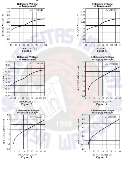
Typical Performance Characteristics
Reference Voltage Reference Voltage vs Temperature vs Temperature
Figure 8. Figure 9.
Reference Voltage Δ Reference Voltage vs Temperature vs Supply Voltage
Figure 10. Figure 11.
Δ Reference Voltage Δ Reference Voltage vs Supply Voltage vs Supply Voltage
LM1577, LM2577
LM1577, LM2577
SNOS658D – JUNE 1999 – REVISED APRIL 2013 www.ti.com
Typical Performance Characteristics (continued)
Error Amp Transconductance Error Amp Transconductance vs Temperature vs Temperature
Figure 14. Figure 15.
Error Amp Voltage Gain Error Amp Transconductance vs
vs Temperature Temperature
Figure 16. Figure 17. Error
Amp Voltage Error Amp Voltage Gain Gain
vs vs Temperature Temperature
LM1577, LM2577
LM1577, LM2577
www.ti.com SNOS658D – JUNE 1999 – REVISED APRIL 2013
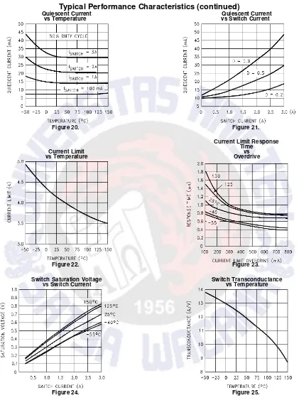
Typical Performance Characteristics (continued)
Quiescent Current Quiescent Current vs Temperature vs Switch Current
Figure 20. Figure 21.
Current Limit Response Time
Current Limit vs vs Temperature Overdrive
Figure 22. Figure 23.
Switch Saturation Voltage Switch Transconductance vs Switch Current vs Temperature
LM1577, LM2577
LM1577, LM2577
SNOS658D – JUNE 1999 – REVISED APRIL 2013 www.ti.com
Typical Performance Characteristics (continued)
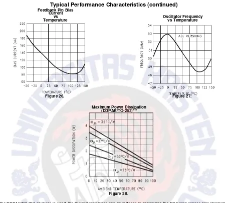
Feedback Pin Bias Current
vs Oscillator Frequency Temperature vs Temperature
Figure 26. Figure 27.
Maximum Power Dissipation (DDPAK/TO-263) (1)
Figure 28.
LM1577, LM2577
LM1577, LM2577
SNOS658D – JUNE 1999 – REVISED APRIL 2013 www.ti.com
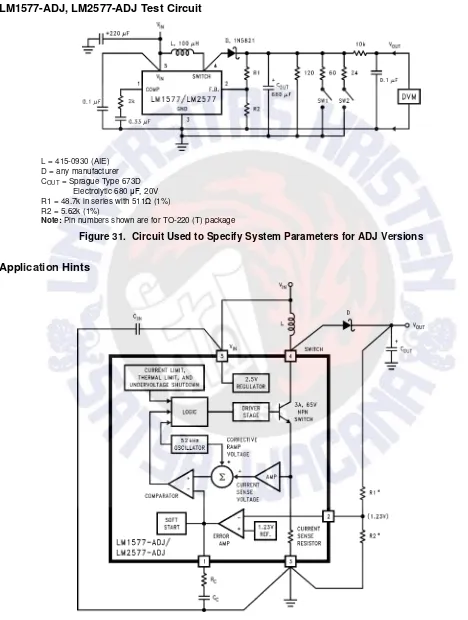
LM1577-ADJ, LM2577-ADJ Test Circuit
L = 415-0930 (AIE) D = any manufacturer COUT = Sprague Type 673D
Electrolytic 680 μF, 20V R1 = 48.7k in series with 511Ω (1%) R2 = 5.62k (1%)
Note: Pin numbers shown are for TO-220 (T) package
Figure 31. Circuit Used to Specify System Parameters for ADJ Versions
LM1577, LM2577
LM1577, LM2577
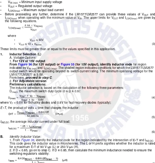
Note: Pin numbers shown are for TO-220 (T) package
*Resistors are internal to LM1577/LM2577 for 12V and 15V versions.
LM1577, LM2577
www.ti.com SNOS658D – JUNE 1999 – REVISED APRIL 2013
LM1577, LM2577
SNOS658D – JUNE 1999 – REVISED APRIL 2013 www.ti.com
STEP-UP (BOOST) REGULATOR
Figure 32 shows the LM1577-ADJ/LM2577-ADJ used as a Step-Up Regulator. This is a switching regulator used
for producing an output voltage greater than the input supply voltage. The LM1577-12/LM2577-12 and LM1577- 15/LM2577-15 can also be used for step-up regulators with 12V or 15V outputs (respectively), by tying the feedback pin directly to the regulator output.
A basic explanation of how it works is as follows. The LM1577/LM2577 turns its output switch on and off at a frequency of 52 kHz, and this creates energy in the inductor (L). When the NPN switch turns on, the inductor current charges up at a rate of VIN/L, storing current in the inductor. When the switch turns off, the lower end of the inductor flies above VIN, discharging its current through diode (D) into the output capacitor (COUT) at a rate of
(VOUT − VIN)/L. Thus, energy stored in the inductor during the switch on time is transferred to the output during the switch off time. The output voltage is controlled by the amount of energy transferred which, in turn, is controlled by modulating the peak inductor current. This is done by feeding back a portion of the output voltage to the error amp, which amplifies the difference between the feedback voltage and a 1.230V reference. The error amp output voltage is compared to a voltage proportional to the switch current (i.e., inductor current during the switch on time).
The comparator terminates the switch on time when the two voltages are equal, thereby controlling the peak switch current to maintain a constant output voltage.
Voltage and current waveforms for this circuit are shown in Figure 33, and formulas for calculating them are given in Table 1.
Figure 33. Step-Up Regulator Waveforms
Table 1. Step-Up Regulator Formulas (1)
Duty Cycle D
Average Inductor Current I IND(AVE)
Inductor Current Ripple Δ IIND
Peak Inductor Current
IIND(PK)
Peak Switch Current I
SW(PK)
Switch Voltage When Off VSW(OFF) VOUT + VF
Diode Reverse Voltage VR VOUT − VSAT
Average Diode Current ID(AVE) ILOAD
Peak Diode Current
LM1577, LM2577
www.ti.com SNOS658D – JUNE 1999 – REVISED APRIL 2013
LM1577, LM2577
SNOS658D – JUNE 1999 – REVISED APRIL 2013 www.ti.com
STEP-UP REGULATOR DESIGN PROCEDURE
The following design procedure can be used to select the appropriate external components for the circuit in
Figure 32, based on these system requirements.
Given:
• VIN (min) = Minimum input supply voltage
• VOUT = Regulated output voltage
• ILOAD(max) = Maximum output load current
• Before proceeding any further, determine if the LM1577/LM2577 can provide these values of VOUT and ILOAD(max) when operating with the minimum value of VIN. The upper limits for VOUT and ILOAD(max) are given by
the following equations.
where
• VOUT ≤ 60V
• VOUT ≤ 10 × VIN(min) (3) These limits must be greater than or equal to the values specified in this application.
1. Inductor Selection (L)
A. Voltage Options: 1. For 12V or 15V output
From Figure 34 (for 12V output) or Figure 35 (for 15V output), identify inductor code for region indicated by VIN (min) and ILOAD (max). The shaded region indicates conditions for which the LM1577/LM2577
output switch would be operating beyond its switch current rating. The minimum operating voltage for the LM1577/LM2577 is 3.5V.
From here, proceed to step C. 2. For Adjustable version Preliminary calculations:
The inductor selection is based on the calculation of the following three parameters: D(max), the maximum switch duty cycle (0 ≤ D ≤ 0.9):
where VF = 0.5V for Schottky diodes and 0.8V for fast recovery diodes (typically);
E •T, the product of volts × time that charges the inductor:
IIND,DC, the average inductor current under full load;
B. Identify Inductor Value:
(4)
(5)
(6)
1. From Figure 36, identify the inductor code for the region indicated by the intersection of E•T and IIND,DC. This code gives the inductor value in microhenries. The L or H prefix signifies whether the inductor is rated for a maximum E•T of 90 V•μs (L) or 250 V•μs (H).
2. If D < 0.85, go on to step C. If D ≥ 0.85, then calculate the minimum inductance needed to ensure the switching regulator's stability:
(7)
If LMIN is smaller than the inductor value found in step B1, go on to step C. Otherwise, the inductor value found in
step B1 is too low; an appropriate inductor code should be obtained from the graph as follows:
LM1577, LM2577
www.ti.com SNOS658D – JUNE 1999 – REVISED APRIL 2013
LM1577, LM2577
SNOS658D – JUNE 1999 – REVISED APRIL 2013 www.ti.com
2. Find where E•T intersects this inductor value to determine if it has an L or H prefix. If E•T intersects both the L and H regions, select the inductor with an H prefix.
Figure 34. LM2577-12 Inductor Selection Guide
LM1577, LM2577
www.ti.com SNOS658D – JUNE 1999 – REVISED APRIL 2013
LM1577, LM2577
SNOS658D – JUNE 1999 – REVISED APRIL 2013 www.ti.com
Note: These charts assume that the inductor ripple current is approximately 20% to 30% of the average inductor current (when the regulator is under full load). Greater ripple current causes higher peak switch currents and greater output ripple voltage; lower ripple current is achieved with larger-value inductors. The factor of 20 to 30% is chosen as a convenient balance between the two extremes.
Figure 36. LM1577-ADJ/LM2577-ADJ Inductor Selection Graph
C. Select an inductor from Table 2 which cross-references the inductor codes to the part numbers of three different manufacturers. Complete specifications for these inductors are available from the respective manufacturers. The inductors listed in this table have the following characteristics:
• AIE: ferrite, pot-core inductors; Benefits of this type are low electro-magnetic interference (EMI), small physical size, and very low power dissipation (core loss). Be careful not to operate these inductors too far beyond their maximum ratings for E•T and peak current, as this will saturate the core.
• Pulse: powdered iron, toroid core inductors; Benefits are low EMI and ability to withstand E•T and peak current above rated value better than ferrite cores.
• Renco: ferrite, bobbin-core inductors; Benefits are low cost and best ability to withstand E•T and peak current above rated value. Be aware that these inductors generate more EMI than the other types, and
LM1577, LM2577
www.ti.com SNOS658D – JUNE 1999 – REVISED APRIL 2013
LM1577, LM2577
SNOS658D – JUNE 1999 – REVISED APRIL 2013 www.ti.com
Table 2. Table of Standardized Inductors and Manufacturer's Part Numbers (1)
Inductor Manufacturer's Part Number
Code Schott Pulse Renco
L47 67126980 PE - 53112 RL2442
L68 67126990 PE - 92114 RL2443
L100 67127000 PE - 92108 RL2444
L150 67127010 PE - 53113 RL1954
L220 67127020 PE - 52626 RL1953
L330 67127030 PE - 52627 RL1952
L470 67127040 PE - 53114 RL1951
L680 67127050 PE - 52629 RL1950
H150 67127060 PE - 53115 RL2445
H220 67127070 PE - 53116 RL2446
H330 67127080 PE - 53117 RL2447
H470 67127090 PE - 53118 RL1961
H680 67127100 PE - 53119 RL1960
H1000 67127110 PE - 53120 RL1959
H1500 67127120 PE - 53121 RL1958
H2200 67127130 PE - 53122 RL2448
(1) Schott Corp., (612) 475-1173
1000 Parkers Lake Rd., Wayzata, MN 55391
Pulse Engineering, (619) 268-2400 P.O. Box 12235, San Diego, CA 92112
Renco Electronics Inc., (516) 586-5566 60 Jeffryn Blvd. East, Deer Park, NY 11729
2. Compensation Network (RC, CC) and Output Capacitor (COUT) Selection
RC and CC form a pole-zero compensation network that stabilizes the regulator. The values of RC and CC are mainly dependant on the regulator voltage gain, ILOAD(max), L and COUT. The following procedure calculates values
for RC, CC, and COUT that ensure regulator stability. Be aware that this procedure doesn't necessarily result in RC
and CC that provide optimum compensation. In order to ensure optimum compensation, one of the standard
procedures for testing loop stability must be used, such as measuring VOUT transient response when pulsing
ILOAD (see Figure 39).
A. First, calculate the maximum value for RC.
Select a resistor less than or equal to this value, and it should also be no greater than 3 kΩ.
B. Calculate the minimum value for COUT using the following two equations.
The larger of these two values is the minimum value that ensures stability.
C. Calculate the minimum value of C .
(8)
LM1577, LM2577
www.ti.com SNOS658D – JUNE 1999 – REVISED APRIL 2013
LM1577, LM2577
SNOS658D – JUNE 1999 – REVISED APRIL 2013 www.ti.com
The compensation capacitor is also part of the soft start circuitry. When power to the regulator is turned on, the switch duty cycle is allowed to rise at a rate controlled by this capacitor (with no control on the duty cycle, it would immediately rise to 90%, drawing huge currents from the input power supply). In order to operate properly, the soft start circuit requires CC ≥ 0.22 μF.
The value of the output filter capacitor is normally large enough to require the use of aluminum electrolytic capacitors. Table 3 lists several different types that are recommended for switching regulators, and the following parameters are used to select the proper capacitor.
Working Voltage (WVDC): Choose a capacitor with a working voltage at least 20% higher than the regulator output voltage.
Ripple Current: This is the maximum RMS value of current that charges the capacitor during each switching cycle. For step-up and flyback regulators, the formula for ripple current is
Choose a capacitor that is rated at least 50% higher than this value at 52 kHz.
(11)
Equivalent Series Resistance (ESR) : This is the primary cause of output ripple voltage, and it also affects the values of RC and CC needed to stabilize the regulator. As a result, the preceding calculations for CC and RC are
only valid if ESR doesn't exceed the maximum value specified by the following equations.
(12)
Select a capacitor with ESR, at 52 kHz, that is less than or equal to the lower value calculated. Most electrolytic capacitors specify ESR at 120 Hz which is 15% to 30% higher than at 52 kHz. Also, be aware that ESR increases by a factor of 2 when operating at −20°C.
In general, low values of ESR are achieved by using large value capacitors (C ≥ 470 μF), and capacitors with high WVDC, or by paralleling smaller-value capacitors.
3. Output Voltage Selection (R1 and R2)
This section is for applications using the LM1577-ADJ/LM2577-ADJ. Skip this section if the LM1577-12/LM2577- 12 or LM1577-15/LM2577-15 is being used.
With the LM1577-ADJ/LM2577-ADJ, the output voltage is given by
VOUT = 1.23V (1 + R1/R2) (13)
Resistors R1 and R2 divide the output down so it can be compared with the LM1577-ADJ/LM2577-ADJ internal 1.23V reference. For a given desired output voltage VOUT, select R1 and R2 so that
4. Input Capacitor Selection (CIN)
(14)
Table 3. Aluminum Electrolytic Capacitors Recommended for Switching Regulators
Cornell Dublier —Types 239, 250, 251, UFT, 300, or 350 P.O. Box 128, Pickens, SC 29671 (803) 878-6311
Nichicon —Types PF, PX, or PZ 927 East Parkway, Schaumburg, IL 60173 (708) 843-7500
Sprague —Types 672D, 673D, or 674D Box 1, Sprague Road, Lansing, NC 28643 (919) 384-2551
United Chemi-Con —Types LX, SXF, or SXJ 9801 West Higgins Road, Rosemont, IL 60018 (708) 696-2000
If the LM1577 is located far from the supply source filter capacitors, an additional large electrolytic capacitor (e.g. 47 μF) is often required.
5. Diode Selection (D)
The switching diode used in the boost regulator must withstand a reverse voltage equal to the circuit output voltage, and must conduct the peak output current of the LM2577. A suitable diode must have a minimum reverse breakdown voltage greater than the circuit output voltage, and should be rated for average and peak current greater than ILOAD(max) and ID(PK). Schottky barrier diodes are often favored for use in switching regulators.
Their low forward voltage drop allows higher regulator efficiency than if a (less expensive) fast recovery diode was used. See Table 4 for recommended part numbers and voltage ratings of 1A and 3A diodes.
Table 4. Diode Selection Chart
VOUT Schottky Fast Recovery
(max) 1A 3A 1A 3A
20V 1N5817 1N5820
MBR120P MBR320P
1N5818 1N5821
30V MBR130P MBR330P
11DQ03 31DQ03
1N5819 1N5822
40V MBR140P MBR340P
11DQ04 31DQ04
MBR150 MBR350 1N4933
50V 11DQ05 31DQ05 MUR105
1N4934 MR851
100V HER102 30DL1
MUR110 MR831