Quartus II Introduction Using Schematic Design
This tutorial presents an introduction to the QuartusR II CAD system. It gives a general overview of a typi-cal CAD flow for designing circuits that are implemented by using FPGA devices, and shows how this flow is realized in the Quartus II software. The design process is illustrated by giving step-by-step instructions for using the Quartus II software to implement a very simple circuit in an Altera FPGA device.
The Quartus II system includes full support for all of the popular methods of entering a description of the desired circuit into a CAD system. This tutorial makes use of the schematic design entry method, in which the user draws a graphical diagram of the circuit. Two other versions of this tutorial are also available, which use the Verilog and VHDL hardware description languages, respectively.
The last step in the design process involves configuring the designed circuit in an actual FPGA device. To show how this is done, it is assumed that the user has access to the Altera DE2 Development and Education board connected to a computer that has Quartus II software installed. A reader who does not have access to the DE2 board will still find the tutorial useful to learn how the FPGA programming and configuration task is performed.
The screen captures in the tutorial were obtained using the Quartus II version 8.0; if other versions of the software are used, some of the images may be slightly different.
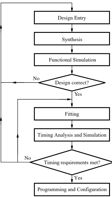
Computer Aided Design (CAD) software makes it easy to implement a desired logic circuit by using a pro-grammable logic device, such as a field-propro-grammable gate array (FPGA) chip. A typical FPGA CAD flow is illustrated in Figure 1.
• Design Entry – the desired circuit is specified either by means of a schematic diagram, or by using a hardware description language, such as Verilog or VHDL
• Synthesis– the entered design is synthesized into a circuit that consists of the logic elements (LEs) provided in the FPGA chip
• Fitting– the CAD Fitter tool determines the placement of the LEs defined in the netlist into the LEs in an actual FPGA chip; it also chooses routing wires in the chip to make the required connections between specific LEs
• Timing Analysis– propagation delays along the various paths in the fitted circuit are analyzed to provide an indication of the expected performance of the circuit
• Timing Simulation– the fitted circuit is tested to verify both its functional correctness and timing
• Programming and Configuration– the designed circuit is implemented in a physical FPGA chip by pro-gramming the configuration switches that configure the LEs and establish the required wiring connections
This tutorial introduces the basic features of the Quartus II software. It shows how the software can be used to design and implement a circuit specified by means of a schematic diagram. It makes use of the graphical user interface to invoke the Quartus II commands. Doing this tutorial, the reader will learn about:
• Creating a project
• Entering a schematic diagram
• Synthesizing a circuit from the schematic diagram
• Fitting a synthesized circuit into an Altera FPGA
• Assigning the circuit inputs and outputs to specific pins on the FPGA
• Simulating the designed circuit
• Programming and configuring the FPGA chip on Altera’s DE2 board
1
Getting Started
Each logic circuit, or subcircuit, being designed with Quartus II software is called aproject. The software works on one project at a time and keeps all information for that project in a single directory (folder) in the file system. To begin a new logic circuit design, the first step is to create a directory to hold its files. To hold the design files for this tutorial, we will use a directoryintrotutorial. The running example for this tutorial is a simple circuit for two-way light control.
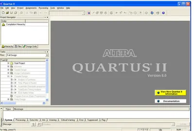
Start the Quartus II software. You should see a display similar to the one in Figure 2. This display consists of several windows that provide access to all the features of Quartus II software, which the user selects with the computer mouse. Most of the commands provided by Quartus II software can be accessed by using a set of menus that are located below the title bar. For example, in Figure 2 clicking the left mouse button on the menu named
For some commands it is necessary to access two or more menus in sequence. We use the conventionMenu1
>Menu2>Itemto indicate that to select the desired command the user should first click the left mouse button onMenu1, then within this menu click onMenu2, and then withinMenu2click onItem. For example,File>
Exituses the mouse to exit from the system. Many commands can be invoked by clicking on an icon displayed in one of the toolbars. To see the command associated with an icon, position the mouse over the icon and a tooltip will appear that displays the command name.
1.1
Quartus II Online Help
Quartus II software provides comprehensive online documentation that answers many of the questions that may arise when using the software. The documentation is accessed from theHelpmenu. To get some idea of the extent of documentation provided, it is worthwhile for the reader to browse through theHelpmenu. For instance, selectingHelp>How to Use Helpgives an indication of what type of help is provided.
The user can quickly search through the Help topics by selectingHelp>Search, which opens a dialog box into which keywords can be entered. Another method, context-sensitive help, is provided for quickly finding documentation for specific topics. While using most applications, pressing theF1function key on the keyboard opens a Help display that shows the commands available for the application.
2
Starting a New Project
To start working on a new design we first have to define a newdesign project. Quartus II software makes the designer’s task easy by providing support in the form of awizard. Create a new project as follows:
1. SelectFile>New Project Wizardto reach the window in Figure 4, which asks for the name and directory of the project.
2. Set the working directory to be introtutorial; of course, you can use some other directory name of your choice if you prefer. The project must have a name, which is usually the same as the top-level design entity that will be included in the project. Chooselightas the name for both the project and the top-level entity, as shown in Figure 4. PressNext. Since we have not yet created the directoryintrotutorial, Quartus II software displays the pop-up box in Figure 5 asking if it should create the desired directory. ClickYes, which leads to the window in Figure 6.
Figure 5. Quartus II software can create a new directory for the project.
Figure 6. The wizard can include user-specified design files.
Figure 7. Choose the device family and a specific device.
Figure 8. Other EDA tools can be specified.
5. The user can specify any third-party tools that should be used. A commonly used term for CAD software for electronic circuits isEDA tools, where the acronym stands for Electronic Design Automation. This term is used in Quartus II messages that refer to third-party tools, which are the tools developed and marketed by companies other than Altera. Since we will rely solely on Quartus II tools, we will not choose any other tools. PressNext.
Figure 9. Summary of the project settings.
3
Design Entry Using the Graphic Editor
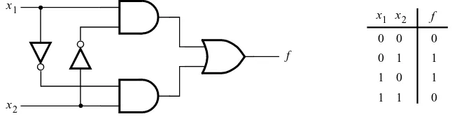
As a design example, we will use the two-way light controller circuit shown in Figure 11. The circuit can be used to control a single light from either of the two switches,x1andx2, where a closed switch corresponds to the logic value 1. The truth table for the circuit is also given in the figure. Note that this is just the Exclusive-OR function of the inputsx1andx2, but we will implement it using the gates shown.
f
The Quartus II Graphic Editor can be used to specify a circuit in the form of a block diagram. SelectFile
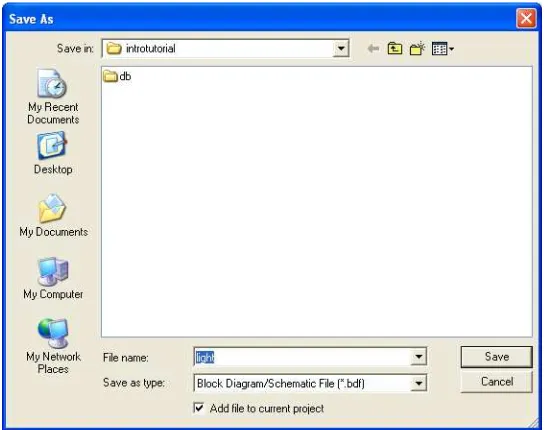
>Newto get the window in Figure 12, chooseBlock Diagram/Schematic File, and clickOK. This opens the Graphic Editor window. The first step is to specify a name for the file that will be created. SelectFile>Save Asto open the pop-up box depicted in Figure 13. In the box labeledSave as typechooseBlock Diagram/Schematic File (*.bdf). In the box labeledFile nametypelight, to match the name given in Figure 4, which was specified when the project was created. Put a checkmark in the boxAdd file to current project. ClickSave, which puts the file into the directoryintrotutorialand leads to the Graphic Editor window displayed in Figure 14.
Figure 13. Name the file.
Figure 14. Graphic Editor window.
3.1
Importing Logic-Gate Symbols
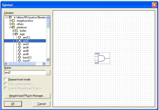
gate symbol will appear in the Graphic Editor window. Using the mouse, move the symbol to a desirable location and click to place it there. Import the second AND gate, which can be done simply by positioning the mouse pointer over the existing AND-gate symbol, right-clicking, and dragging to make a copy of the symbol. A symbol in the Graphic Editor window can be moved by clicking on it and dragging it to a new location with the mouse button pressed. Next, selector2from the library and import the OR gate into the diagram. Then, selectnotand import two instances of the NOT gate. Rotate the NOT gates into proper position by using the “Rotate left 90" icon . Arrange the gates as shown in Figure 16.
Figure 15. Choose a symbol from the library.
3.2
Importing Input and Output Symbols
Having entered the logic-gate symbols, it is now necessary to enter the symbols that represent the input and output ports of the circuit. Use the same procedure as for importing the gates, but choose the port symbols from the libraryprimitives/pin. Import two instances of the input port and one instance of the output port, to obtain the image in Figure 17.
Figure 17. Import the input and output pins.
Assign names to the input and output symbols as follows. Make sure nothing is selected by clicking on an empty spot in the Graphic Editor window. Point to the wordpin_nameon the top input symbol and double-click the mouse. The dialog box in Figure 18 will appear. Type the pin name,x1, and clickOK. Similarly, assign the namex2to the other input andf to the output. Alternatively, it is possible to change the name of an element by selecting it first, and then double-clicking on the name and typing a new one directly.
3.3
Connecting Nodes with Wires
The symbols in the diagram have to be connected by drawing lines (wires). Click on the icon in the toolbar to activate the Orthogonal Node Tool. Position the mouse pointer over the right edge of thex1input pin. Click and hold the mouse button and drag the mouse to the right until the drawn line reaches the pinstub on the top input of the AND gate. Release the mouse button, which leaves the line connecting the two pinstubs. Next, draw a wire from the input pinstub of the leftmost NOT gate to touch the wire that was drawn above it. Note that a dot will appear indicating a connection between the two wires.
Use the same procedure to draw the remaining wires in the circuit. If a mistake is made, a wire can be selected by clicking on it, and removed by pressing the Delete key on the keyboard. Upon completing the diagram, click on the icon , to activate the Selection Tool. Now, changes in the appearance of the diagram can be made by selecting a particular symbol or wire and either moving it to a different location or deleting it. The final diagram is shown in Figure 19; save it.
Figure 19. The completed schematic diagram.
4
Compiling the Designed Circuit
The entered schematic diagram file,light.bdf, is processed by several Quartus II tools that analyze the file, syn-thesize the circuit, and generate an implementation of it for the target chip. These tools are controlled by the application program called theCompiler.
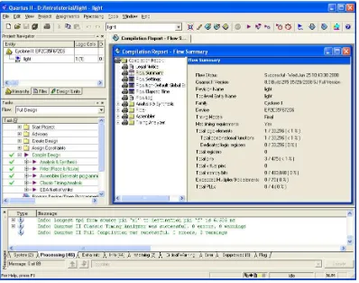
Run the Compiler by selectingProcessing>Start Compilation, or by clicking on the toolbar icon that looks like a purple triangle. As the compilation moves through various stages, its progress is reported in a window on the left side of the Quartus II display. Successful (or unsuccessful) compilation is indicated in a pop-up box. Acknowledge it by clickingOK, which leads to the Quartus II display in Figure 20. In the message window, at the bottom of the figure, various messages are displayed. In case of errors, there will be appropriate messages given.
4.1
Errors
Quartus II software displays messages produced during compilation in the Messages window. If the block diagram design file is correct, one of the messages will state that the compilation was successful and that there are no errors. If the Compiler does not report zero errors, then there is at least one mistake in the schematic entry. In this case a message corresponding to each error found will be displayed in the Messages window. Double-clicking on an error message will highlight the offending part of the circuit in the Graphic Editor window. Similarly, the Compiler may display some warning messages. Their details can be explored in the same way as in the case of error messages. The user can obtain more information about a specific error or warning message by selecting the message and pressing theF1function key.
To see the effect of an error, open the filelight.bdf. Remove the wire connecting the output of the top AND gate to the OR gate. To do this, click on the icon, click the mouse on the wire to be removed (to select it) and press Delete. Compile the erroneous design by clicking on the icon. A pop-up box will ask if the changes made to thelight.bdffile should be saved; clickYes. After trying to compile the circuit, Quartus II software will display a pop-up box indicating that the compilation was not successful. Acknowledge it by clickingOK. The compilation report summary, given in Figure 21, now confirms the failed result. Expand theAnalysis & Synthesispart of the report and then selectMessagesto have the messages displayed as shown in Figure 22. Double-click on the first error message, which states that one of the nodes is missing a source. Quartus II software responds by displaying thelight.bdfschematic and highlighting the OR gate which is affected by the error, as shown in Figure 23. Correct the error and recompile the design.
Figure 22. Error messages.
Figure 23. Identifying the location of the error.
5
Pin Assignment
During the compilation above, the Quartus II Compiler was free to choose any pins on the selected FPGA to serve as inputs and outputs. However, the DE2 board has hardwired connections between the FPGA pins and the other components on the board. We will use two toggle switches, labeledSW0andSW1, to provide the external inputs,
Figure 24. The Assignment Editor window.
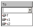
Pin assignments are made by using the Assignment Editor. SelectAssignments>Assignment Editor to reach the window in Figure 24. UnderCategoryselectPin. Double-click on the entry<<new>>which is highlighted in blue in the column labeled To. The drop-down menu in Figure 25 will appear. Click onx1as the first pin to be assigned; this will enterx1in the displayed table. Follow this by double-clicking on the box to the right of this newx1entry, in the column labeled Location. Now, the drop-down menu in Figure 26 appears. Scroll down and selectPIN_N25. Instead of scrolling down the menu to find the desired pin, you can just type the name of the pin (N25) in the Location box. Use the same procedure to assign inputx2to pin N26 and outputf to pin AE22, which results in the image in Figure 27. To save the assignments made, chooseFile>Save. You can also simply close the Assignment Editor window, in which case a pop-up box will ask if you want to save the changes to assignments; clickYes. Recompile the circuit, so that it will be compiled with the correct pin assignments.
Figure 27. The complete assignment.
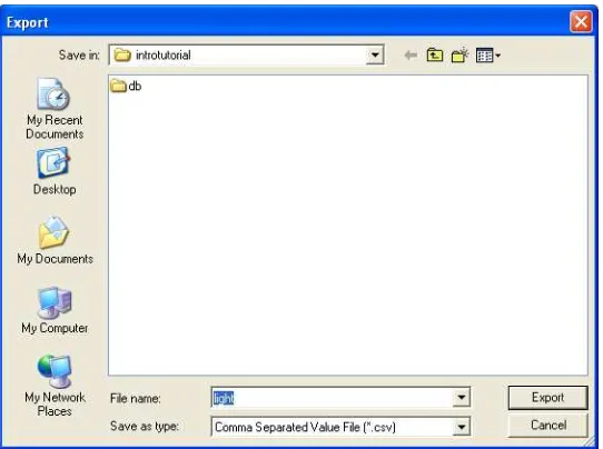
The DE2 board has fixed pin assignments. Having finished one design, the user will want to use the same pin assignment for subsequent designs. Going through the procedure described above becomes tedious if there are many pins used in the design. A useful Quartus II feature allows the user to both export and import the pin assignments from a special file format, rather than creating them manually using the Assignment Editor. A simple file format that can be used for this purpose is thecomma separated value (CSV)format, which is a common text file format that contains comma-delimited values. This file format is often used in conjunction with the Microsoft Excel spreadsheet program, but the file can also be created by hand using any plain ASCII text editor. The format for the file for our simple project is
To, Location x1, PIN_N25 x2, PIN_N26 f, PIN_AE22
By adding lines to the file, any number of pin assignments can be created. Suchcsvfiles can be imported into any design project.
If you created a pin assignment for a particular project, you can export it for use in a different project. To see how this is done, open again the Assignment Editor to reach the window in Figure 27. Now, selectFile>Export
Figure 28. Exporting the pin assignment.
You can import a pin assignment by choosingAssignments>Import Assignments. This opens the dia-logue in Figure 29 to select the file to import. Type the name of the file, including thecsvextension and the full path to the directory that holds the file, in the File Name box and pressOK. Of course, you can also browse to find the desired file.
Figure 29. Importing the pin assignment.
6
Simulating the Designed Circuit
Before implementing the designed circuit in the FPGA chip on the DE2 board, it is prudent to simulate it to ascertain its correctness. Quartus II software includes a simulation tool that can be used to simulate the behavior of a designed circuit. Before the circuit can be simulated, it is necessary to create the desired waveforms, called test vectors, to represent the input signals. It is also necessary to specify which outputs, as well as possible internal points in the circuit, the designer wishes to observe. The simulator applies the test vectors to a model of the implemented circuit and determines the expected response. We will use the Quartus II Waveform Editor to draw the test vectors, as follows:
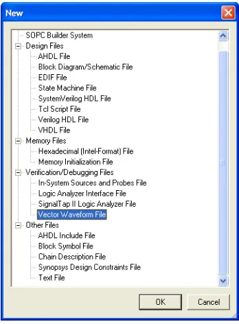
1. Open the Waveform Editor window by selectingFile>New, which gives the window shown in Figure 30. ChooseVector Waveform Fileand clickOK.
Figure 30. Need to prepare a new file.
2. The Waveform Editor window is depicted in Figure 31. Save the file under the namelight.vwf; note that this changes the name in the displayed window. Set the desired simulation to run from 0 to 200 ns by selecting
Edit>End Timeand entering 200 ns in the dialog box that pops up. SelectingView>Fit in Window
Figure 31. The Waveform Editor window.
Figure 32. The augmented Waveform Editor window.
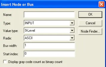
3. Next, we want to include the input and output nodes of the circuit to be simulated. ClickEdit>Insert>
Figure 34. Selecting nodes to insert into the Waveform Editor.
Click on thex1signal in the Nodes Found box in Figure 34, and then click the>sign to add it to the Selected Nodes box on the right side of the figure. Do the same forx2andf. ClickOKto close the Node Finder window, and then clickOKin the window of Figure 33. This leaves a fully displayed Waveform Editor window, as shown in Figure 35. If you did not select the nodes in the same order as displayed in Figure 35, it is possible to rearrange them. To move a waveform up or down in the Waveform Editor window, click on the node name (in the Name column) and release the mouse button. The waveform is now highlighted to show the selection. Click again on the waveform and drag it up or down in the Waveform Editor.
Figure 35. The nodes needed for simulation.
To simulate the behavior of a large circuit, it is necessary to apply a sufficient number of input valuations and observe the expected values of the outputs. In a large circuit the number of possible input valuations may be huge, so in practice we choose a relatively small (but representative) sample of these input valuations. However, for our tiny circuit we can simulate all four input valuations given in Figure 11. We will use four 50-ns time intervals to apply the four test vectors.
We can generate the desired input waveforms as follows. Click on the waveform name for thex1node. Once a waveform is selected, the editing commands in the Waveform Editor can be used to draw the desired waveforms. Commands are available for setting a selected signal to 0, 1, unknown (X), high impedance (Z), don’t care (DC), inverting its existing value (INV), or defining a clock waveform. Each command can be activated by using theEdit>Valuecommand, or via the toolbar for the Waveform Editor. The Edit menu can also be opened by right-clicking on a waveform name.
Setx1to 0 in the time interval 0 to 100 ns, which is probably already set by default. Next, setx1to 1 in the time interval 100 to 200 ns. Do this by pressing the mouse at the start of the interval and dragging it to its end, which highlights the selected interval, and choosing the logic value 1 in the toolbar. Makex2= 1 from 50 to 100 ns and also from 150 to 200 ns, which corresponds to the truth table in Figure 11. This should produce the image in Figure 36. Observe that the outputf is displayed as having an unknown value at this time, which is indicated by a hashed pattern; its value will be determined during simulation. Save the file.
Figure 36. Setting of test values.
6.1
Performing the Simulation
A designed circuit can be simulated in two ways. The simplest way is to assume that logic elements and intercon-nection wires in the FPGA are perfect, thus causing no delay in propagation of signals through the circuit. This is calledfunctional simulation. A more complex alternative is to take all propagation delays into account, which leads totiming simulation. Typically, functional simulation is used to verify the functional correctness of a circuit as it is being designed. This takes much less time, because the simulation can be performed simply by using the logic expressions that define the circuit.
6.1.1 Functional Simulation
by selectingProcessing>Generate Functional Simulation Netlist. A simulation run is started by Process-ing>Start Simulation, or by using the icon . At the end of the simulation, Quartus II software indicates its successful completion and displays a Simulation Report illustrated in Figure 38. If your report window does not show the entire simulation time range, click on the report window to select it and chooseView>Fit in Window. Observe that the outputf is as specified in the truth table of Figure 11.
Figure 37. Specifying the simulation mode.
Figure 38. The result of functional simulation.
6.1.2 Timing Simulation
Settings>Simulator Settingsto get to the window in Figure 37, chooseTimingas the simulation mode, and clickOK. Run the simulator, which should produce the waveforms in Figure 39. Observe that there is a delay of about 6 ns in producing a change in the signalf from the time when the input signals,x1andx2, change their values. This delay is due to the propagation delays in the logic element and the wires in the FPGA device.
Figure 39. The result of timing simulation.
7
Programming and Configuring the FPGA Device
The FPGA device must be programmed and configured to implement the designed circuit. The required configura-tion file is generated by the Quartus II Compiler’s Assembler module. Altera’s DE2 board allows the configuraconfigura-tion to be done in two different ways, known as JTAG and AS modes. The configuration data is transferred from the host computer (which runs the Quartus II software) to the board by means of a cable that connects a USB port on the host computer to the leftmost USB connector on the board. To use this connection, it is necessary to have the USB-Blaster driver installed. If this driver is not already installed, consult the tutorialGetting Started with Altera’s DE2 Boardfor information about installing the driver. Before using the board, make sure that the USB cable is properly connected and turn on the power supply switch on the board.
In the JTAG mode, the configuration data is loaded directly into the FPGA device. The acronym JTAG stands for Joint Test Action Group. This group defined a simple way for testing digital circuits and loading data into them, which became an IEEE standard. If the FPGA is configured in this manner, it will retain its configuration as long as the power remains turned on. The configuration information is lost when the power is turned off. The second possibility is to use the Active Serial (AS) mode. In this case, a configuration device that includes some flash memory is used to store the configuration data. Quartus II software places the configuration data into the configuration device on the DE2 board. Then, this data is loaded into the FPGA upon power-up or reconfiguration. Thus, the FPGA need not be configured by the Quartus II software if the power is turned off and on. The choice between the two modes is made by the RUN/PROG switch on the DE2 board. The RUN position selects the JTAG mode, while the PROG position selects the AS mode.
7.1
JTAG Programming
Figure 40. The Programmer window.
Observe that the configuration filelight.sofis listed in the window in Figure 40. If the file is not already listed, then clickAdd Fileand select it. This is a binary file produced by the Compiler’s Assembler module, which contains the data needed to configure the FPGA device. The extension.sofstands for SRAM Object File. Note also that the device selected is EP2C35F672, which is the FPGA device used on the DE2 board. Click on the
Program/Configurecheck box, as shown in Figure 42.
Figure 41. The Hardware Setup window.
Now, pressStartin the window in Figure 42. An LED on the board will light up when the configuration data has been downloaded successfully. If you see an error reported by Quartus II software indicating that programming failed, then check to ensure that the board is properly powered on.
7.2
Active Serial Mode Programming
In this case, the configuration data has to be loaded into the configuration device on the DE2 board, which is identified by the name EPCS16. To specify the required configuration device selectAssignments>Device, which leads to the window in Figure 43. Click on theDevice and Pin Optionsbutton to reach the window in Figure 44. Now, click on theConfigurationtab to obtain the window in Figure 45. In the Configuration device box (which may be set to Auto) choose EPCS16 and clickOK. Upon returning to the window in Figure 43, click
OK. Recompile the designed circuit.
Figure 44. The Options window.
Figure 45. Specifying the configuration device.
Hardware Setup indicates the USB-Blaster. If the configuration file is not already listed in the window, pressAdd File. The pop-up box in Figure 48 will appear. Select the filelight.pofin the directoryintrotutorial and click
Open. As a result, the configuration filelight.pofwill be listed in the window. This is a binary file produced by the Compiler’s Assembler module, which contains the data to be loaded into the EPCS16 configuration device. The extension.pofstands for Programmer Object File. Upon returning to the Programmer window, click on the
Program/Configurecheck box, as shown in Figure 49.
Figure 46. Clear the previously selected devices.
Figure 49. The updated Programmer window.
Flip the RUN/PROG switch on the DE2 board to the PROG position. PressStartin the window in Figure 49. An LED on the board will light up when the configuration data has been downloaded successfully. Also, the Progress box in Figure 49 will indicate when the configuration and programming process is completed, as shown in Figure 50.
Figure 50. The Programmer window upon completion of programming.
8
Testing the Designed Circuit
Having downloaded the configuration data into the FPGA device, you can now test the implemented circuit. Flip the RUN/PROG switch to RUN position. Try all four valuations of the input variablesx1andx2, by setting the corresponding states of the switchesSW1andSW0. Verify that the circuit implements the truth table in Figure 11.
Copyright c2008 Altera Corporation. All rights reserved. Altera, The Programmable Solutions Company, the stylized Altera logo, specific device designations, and all other words and logos that are identified as trademarks and/or service marks are, unless noted otherwise, the trademarks and service marks of Altera Corporation in the U.S. and other countries. All other product or service names are the property of their respective holders. Altera products are protected under numerous U.S. and foreign patents and pending applications, mask work rights, and copyrights. Altera warrants performance of its semiconductor products to current specifications in accordance with Altera’s standard warranty, but reserves the right to make changes to any products and services at any time without notice. Altera assumes no responsibility or liability arising out of the application or use of any information, product, or service described herein except as expressly agreed to in writing by Altera Corporation. Altera customers are advised to obtain the latest version of device specifications before relying on any published information and before placing orders for products or services.