Introduction
Renewable energy
Solar cells
Transparent solar cells
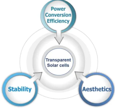
- Important factor to consider for development of transparent solar cells
- Analysis of transparent solar cells
- Performance analysis
- Aesthetics factor evaluation
- Types of the transparent solar cells
- Thin film type
- Selective light-transmission type
- Luminescent solar concentrator type
Transparent solar cells are intended to replace a glass building window or car solar roof. By obtaining CIELAB values, the color of transparent solar cells can be checked.
Transparent crystalline silicon substrates
Introduction
Ultra-thin crystalline silicon substrates
30 wt% potassium hydroxide solution at 90 ℃ for the production of ultra-thin crystalline silicon substrates from a thickness of 100 μm to 20 μm. As shown in Figure 2.1 A, even if we reduce the thickness of crystalline silicon substrate to 10 μm, only a small amount of visible light can penetrate.

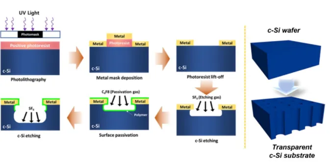
Fabrication of microwire arrays to develop transparent crystalline silicon substrates
- Fabrication of the microwire arrays on glass substrates
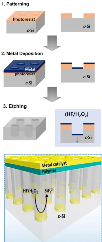
- Fabrication of etching mask (Photolithography process)
- Etching process via deep reactive ion etching
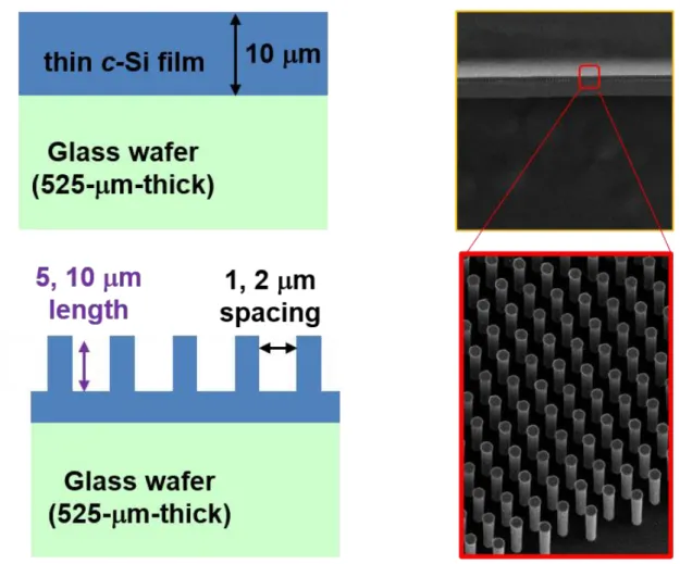
- Crystalline silicon microwires on glass substrates
First, when the crystalline silicon microwire arrays with 2 μm diameter and 2 μm spacing were fabricated on a 10 μm thick crystalline silicon wafer with lengths of 5 μm or 10 μm. In the case of the 5-μm-long crystalline silicon microwire arrays with 5-μm thick crystalline silicon bottom substrate, it was confirmed that the average visible transmission was about 12%.

Fabrication of microhole arrays to develop transparent crystalline silicon substrates
- Design of the transparent crystalline silicon substrate
- Design of the light transmission window diameter
- Design of the spacing between the light transmission windows
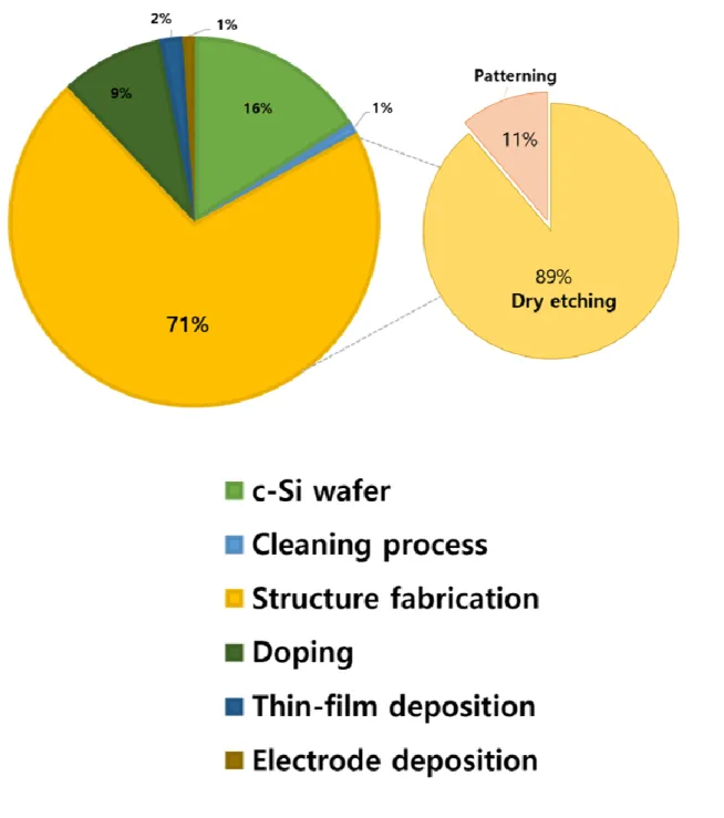
- Fabrication of the transparent crystalline silicon substrate via dry etching process -33
- Fabrication of transparent crystalline silicon via deep reactive ion etching
- Fabrication of the transparent crystalline silicon substrate via wet etching process -38
- Transmittance control of transparent crystalline silicon substrates
- Design of filling fraction of the crystalline silicon substrate
- Design of filling fraction of the crystalline silicon substrate
The crystalline silicon substrate with light transmission windows is gray colored square at the bottom. In this equation, the distance between the human eyes and the transparent crystalline silicon substrate is L, and the spacing between the light transmission windows is s. Therefore, we are trying to fabricate transparent crystalline silicon substrates via a wet etching process called metal-assisted chemical etching.
On the other hand, the developed transparent crystalline silicon substrate shows full transparency like glass (Figure 2.26). The transparent crystalline silicon substrate also ensures that things behind it are clearly visible without cloudiness. The results clearly show that the haze ratio of the crystalline silicon transparent substrate is 0.95%, just like that of glass.
Thus, the permeability of the transparent crystalline silicon substrate can be changed by adjusting the filling ratio of the crystalline silicon substrate. To fabricate a transparent crystalline silicon substrate with transmittance from 20% transmittance to 50% transmittance, the filling fraction was controlled by adjusting the diameter of the light transmittance windows and the spacing between the light transmittance windows and the number of holes. Thus, the possible values of the number of light transmission windows (n) are 1 and 7 when the filling fraction values are 70% and 80% for the development of transparent crystalline silicon substrates with transmittance of 20% and 30%.
A transparent crystalline silicon substrate can be fabricated even if the light transmission windows are arranged in shapes other than the hexagonal pattern. Transparent crystalline silicon substrates were fabricated by forming pinhole windows for light transmission on a 200 μm thick conventional crystalline silicon wafer.
Transparent crystalline silicon solar cells
Fabrication of transparent crystalline silicon solar cells
Optical properties of transparent crystalline silicon solar cells
The current density of transparent crystalline silicon solar cells was again verified by external quantum efficiency (Figure 3.9). The efficiency of solar cells made of transparent crystalline silicon is much higher than that of other transparent solar cells of neutral colors.7,. Therefore, the basic open circuit voltage limits of transparent crystalline silicon solar cells are around 770-780 mV.
Overall, the power conversion efficiency of the transparent crystalline silicon solar cells was lower than the fundamental limit. In addition, the transparent crystalline silicon solar cells are also expected to be commercialized quickly. The first step is to improve the power conversion efficiency of 1 cm x 1 cm transparent crystalline silicon solar cells.
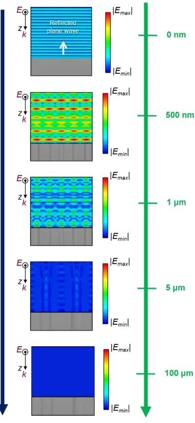
We applied the light-harvesting film (polydimethylsiloxane film with inverted pyramid structure) on transparent crystalline silicon solar cells to improve energy conversion efficiency. In this study, we develop the new manufacturing process for transparent crystalline silicon solar cells with polydimethylsiloxane film. Then finally, we can fabricate a light-collecting film with micro-hole pattern on the transparent crystalline silicon solar cells.
As a result, as shown in Figure 3.30, the transparent crystalline silicon solar cells with films retain transparency. The photovoltaic performance of the transparent crystalline silicon solar cells is higher than the photovoltaic performance of other colorless transparent solar cells reported so far.

Photovoltaic performance of transparent crystalline silicon solar cells
Commercialization possibilities of the transparent crystalline silicon solar cells
In the case of the transparent crystalline silicon solar cells, they not only have a high power conversion efficiency, but also the transparent crystalline silicon solar cells have the potential to be highly stable the same as commercial crystalline silicon solar cells because the structure of the solar cells is very similar. The manufacturing step of a transparent crystalline silicon solar cells is highly compatible with the current commercially available crystalline silicon solar cells. Therefore, the developed transparent solar cell is expected to be commercialized very quickly compared to other types of solar cells.
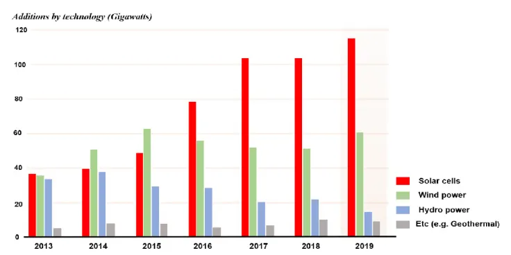
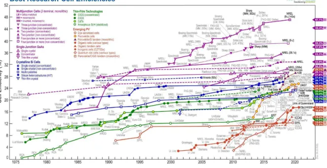
Furthermore, since the process steps are similar, it is a very big advantage that commercial silicon solar cell manufacturing facilities can be used as they are during commercialization. In addition, since the crystalline silicon solar cell already meets the conditions of high efficiency, high stability and reasonable price, it occupies more than 90% of the current solar cell market, as can be seen in Figure 3.12.60 Therefore, the case of the transparent crystalline silicon solar cells, it is expected to occupy a large share of the solar cell market. Then the development of large transparent solar cells with a size of at least 5 cm x 5 cm (25 cm2).
Moreover, the world's first transparent solar window based on transparent crystalline silicon solar cells will be developed through the modularization of transparent solar cells. In the process steps of the transparent crystalline silicon solar cells, steps 1 and 2 can be interchanged, just like in the commercial process steps.

Efficiency enhancement of the transparent solar cells with surface treatment
A more detailed mechanism of HNA etching has been reported by Robbins and Schwartz.64-67 Since the HNA solution has isotropic etching properties, etching occurs in all directions equally, regardless of the crystal direction of crystalline silicon. Due to this characteristic, conformal etching is possible in the defective light transmission area in the areas of transparent crystalline silicon substrates. We conducted a study to remove the surface damage of the light transmission regions of the rates of transparent crystalline silicon substance using RSE-100 (a ratio of HF:HNO3:CH3COOH = 2:7:1), which is a representative HN solution A.
First, to control the etching rate, a transparent crystalline silicon substrate was immersed in the HNA solution (Figure 3.16A). It was also confirmed that the entire sidewall surface of the light transmission windows was smooth, as shown in Figure 3.17. This wet chemical surface treatment not only has the advantage of removing damage to the wall surface as well as the microhole area, but also allows control of the microhole diameter (Figure 3.19).
Finally, the transparent crystalline silicon solar cells fabricated with the transparent crystalline silicon substrate with surface treatment exhibited an open circuit voltage increase of 20 mV compared to that of the transparent crystalline silicon solar cell without surface treatment. Especially when the size of the transparent crystalline silicon solar cells is scaled up as the surface area increases, then the effect of surface treatment becomes more critical. On the other hand, when the transparent crystalline silicon solar cell was produced after surface treatment, the open-circuit voltage increases 100 mV than that of the transparent crystalline silicon solar cell without surface treatment.

Efficiency enhancement of the transparent solar cells with light-harvesting film
This is because the inverted pyramid structure polydimethylsiloxane film with a high haze ratio of over 97% covers the light transmission area of the transparent crystalline silicon solar cells. Therefore, in order to apply the inverted pyramid structured polydimethylsiloxane film to the transparent crystalline silicon solar cells, the inverted pyramid structured polydimethylsiloxane film should only be placed in the light absorption region of the transparent crystalline silicon solar cells. Therefore, to apply the film to transparent crystalline silicon solar cells, the light-harvesting film should only be placed in the light absorption region of transparent crystalline silicon solar cells.
However, to apply microhole patterned textured polydimethylsiloxane film to transparent crystalline silicon solar cells, stretching process is required. In addition, when we check the haze ratio of transparent crystalline silicon solar cells with textured film, it is 1.2% which is almost no transmission haze ratio. In the case of glass and transparent crystalline silicon substrate, the haze ratio is 0.89% and 0.95%, respectively (Figure 3.32).
We checked whether the energy conversion efficiency of the transparent crystalline silicon solar cells is improved by attaching the light collecting film due to the improvement of the current density (Figure 3.33-3.34). As shown in Table 3.6, the transparent crystalline silicon solar cells with a light collecting film exhibit an energy conversion efficiency of 14.6% at a short-circuit current of 30.9 mA/cm2, the open-circuit voltage of 618 mV and a fill current of 618 mV. factor of 76.3%. In the case of the transparent crystalline silicon solar cells without light-collecting film, the device exhibits an energy conversion efficiency of 13.5 with a short-circuit current density of 28.3 mA/cm2, an open-circuit voltage of 618 mV, and a fill factor. of 77.0%.

Conclusion
J.; Seo, K., Cold isostatically printed silver nanowire electrodes for flexible organic solar cells via room temperature processes. Yang, R.; Lee, C.-H.; Cui, B.; Sazonov, A., Flexible semi-transparent a-Si: H-pin solar cells for functional energy harvesting applications. Matsuo, Y., Dual interface modifications enable high performance semitransparent perovskite solar cells with large open circuit voltage and fill factor.
Cho, A.; Yoo, J.-S., Development of semitransparent CIGS thin-film solar cells modified with a sulfide-AgGa layer for construction applications. Horng, S.-F.; Zan, H.-W., Efficient semitransparent organic solar cells with good color perception and good color rendering from blade coating. Li, F.; Xu, Y.; Chen, W.; Xie, S.; Li, J., Enhanced carbon nanotube networks as top electrodes for fully printable mesoscopic semitransparent perovskite solar cells.
H.; Seo, K., Dopant-free all-back-contact Si nanohole solar cells using MoO x and LiF films. Seo* "Dopant-free All-back-contact Si Nanohole Solar Cells using MoOx and LiF Films" Nano Lett. Seo* "Cold isostatic printed silver nanowire electrodes for flexible organic solar cells via room temperature processes" Adv Mater.