Wireless power transfer technology is the technology that has made remarkable progress, primarily in wireless charging for personal portable devices and electric vehicles. Convergence of wireless power transfer technology (WPT) and rechargeable battery can extend the life of BIMD and reduce the suffering and cost of battery replacements.
As the population ages and interest in health grows, research into body implantable medical devices (BIMDs) continues actively. An implantable system such as a pacemaker uses a primary battery for power.
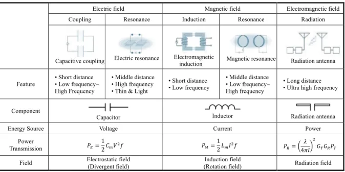
Principle
The induced magnetic field around the closed loop is proportional to the current density plus the time varying current. The time varying current in the primary coil induces a magnetic field and the time varying magnetic field induces current which turns into electromotive force in the secondary coil.
Parameters
- Quality factor
- Coupling coefficient and mutual inductance
The coupling coefficient is described from '0' to '1', where '0' is the magnetic field of the primary coil that has no effect on the secondary coil. Coupling coefficient '1' shows that the magnetic field of the primary coil is fully coupled to the secondary coil.
Types of magnetically coupled WPT
- Magnetic inductive
- Magnetic resonance
Circuit description
- Overall system architecture of wireless power transfer
- Transmitting coil driver
- Rectifier
- DC-DC converter
- Regulator
The waveform of the output voltage, which has voltage drop, is shown in fig. 2.9 (d) with black dotted line. As shown in the last column of fig. 2.13 (d), the input current, IIN, flows only during the charging phase.
Technical challenges in WPT
- Efficiency degradation by coil geometry variation
- Voltage gain variation with coil geometry
- Power loss in receiver circuits
The power loss in the switches can be described as a combination of the switching loss (PSW) and the conduction loss of the MOSFET (PCOND). Similarly, the total power loss in a low MOSFET can be calculated using the same method as a high MOSFET.
Challenges for body implantable medical devices
- Space limitation
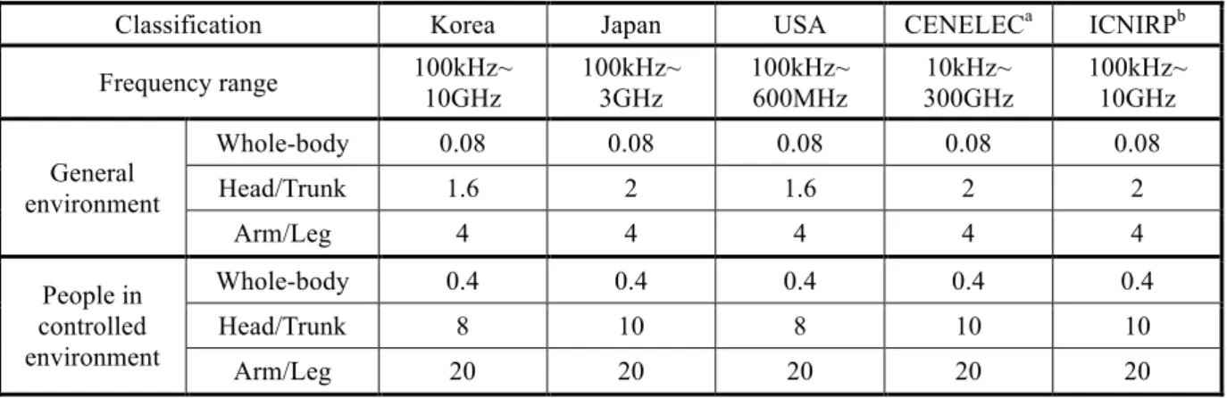
- Human health hazard
- Safe operation
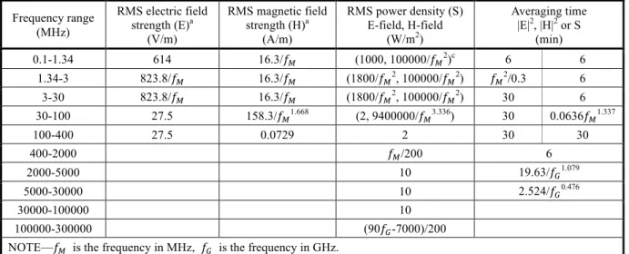
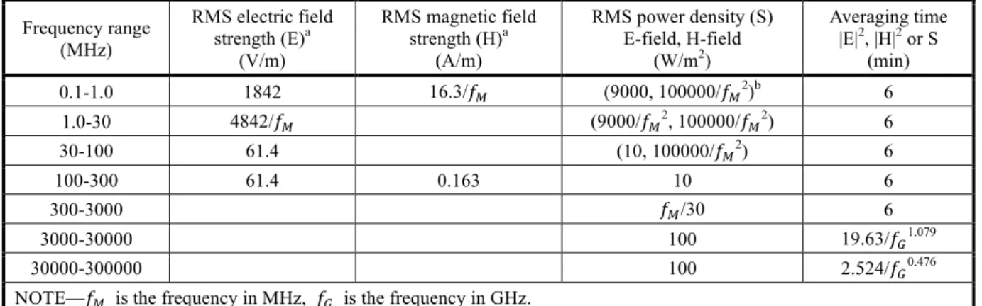
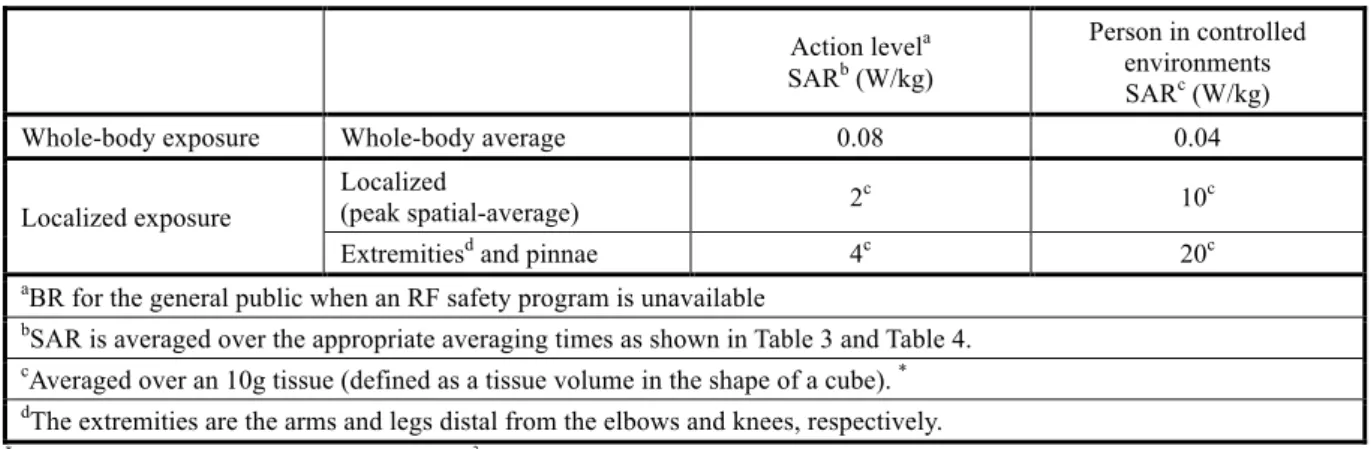
For non-uniform exposures, the mean values of the exposure fields are obtained by spatially averaging the squares of the field strength or averaging the power density over an area equivalent to the vertical cross-section of the human body (the projected area) or a smaller area depending on the frequency (see NOTES to Table 3 and Table 4 below), we compare it with the NDP in the table. For non-uniform exposures, the mean values of the exposure fields are obtained by spatially averaging the squares of the field strength or averaging the power density over an area equal to the vertical cross-section of the human body (projected area) or a smaller area, depending on the frequency (see NOTES to Table 3 and Table 4 below), are compared with the NDP in the table.
Efficiency enhancement in coil geometric variation
- Background
- MR-WPT model analysis
- Power transfer characteristics, and analysis on geometric variation
- Maximum power transfer conditions
- Simulation results
- Performance verification
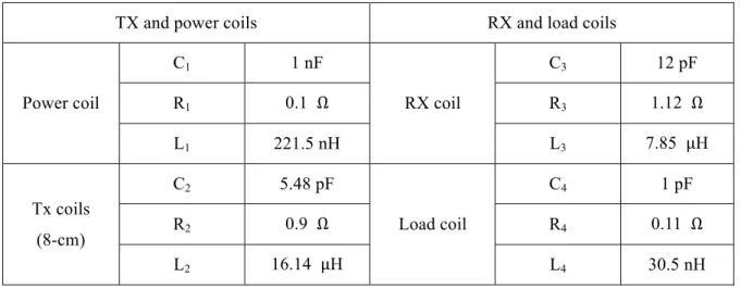
- Coil characteristics
- Experimental settings
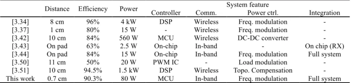
- Experimental results
- Safety check
- Experimental results of effect on real tissue
- Verification on SAR
- Conclusion
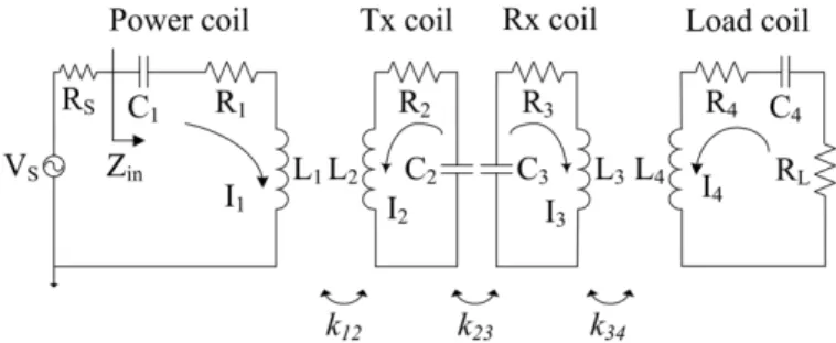
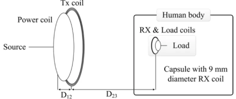
However, a conventional MR-WPT system still suffers from efficiency loss due to changes in receiver position. The circuit analysis focuses on the parameters that influence the coupling coefficient of the MR-WPT system. The proposed model of the MR-WPT A strongly coupled MR-WPT system consists of four coils.
The proposed MR-WPT system model for capsule endoscopy as shown in Figure R6XZLXìîXXJîJX 6Ñ6]ZLXì]êXJ]Jê Z6R6ÑLXìX]XJXJ]0H. 3.4) The efficiency of the WPT system can be expressed by the following equation:. where ñ is the efficiency of the MR-WPT system, and +st and +ùûB are the source power from the supply coil and the transmitted power on the load coil, respectively. When the relative positions of the TX and RX coils change, the changed P1h causes a deterioration of úiI, resulting in reduced power transfer efficiency for the MR-WPT system.
With the circuit model of the MR-WPT system, it is possible to calculate the optimal value of PI1 for a given P1h. Thus, the safety of the proposed MR-WPT system in the human body was confirmed. This confirmed the safety of the proposed MR-WPT system for use in the human body.
Step-charging technique for Li-ion battery charger
- Background
- Frequency modulation for CC and CV modes
- Step-charging technique
- Li-ion battery characteristics
- Step-charging algorithm
- System description
- Transmitter and receiver
- Coil characteristics
- Communication circuits and analysis
- Performance verification
- Experimental settings
- Experimental results
- Conclusion
To implement CC/CV mode, fundamental characteristic of the battery known as voltage hysteresis is used. To implement this technique, the operation of the primary and secondary sides must be synchronized by the algorithm through one-way communication from the secondary to primary side. The battery exhibits hysteresis, shown as a drop in battery voltage proportional to the charging current.
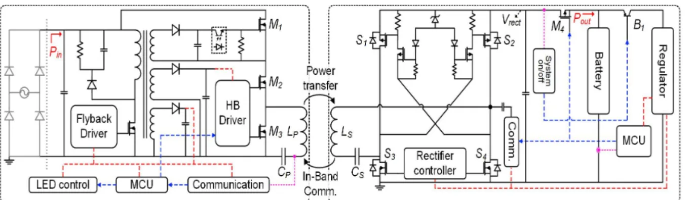
The MCU (AT90PWM) is mainly used to control the power transfer operation between the coils. Figure 3.28(a) shows the primary and secondary side communication circuit where unidirectional in-band communication is used. When T1 and T2 are on, the primary side also senses the change in secondary side impedance.
The loop impedance for the primary side is the same as (3.13), but the secondary side is expressed as Fig.3.32 shows the battery charging waveforms of the proposed wireless battery charger in the time domain. Fig.3.33(b) shows the charging efficiency of the system under CV mode with the battery voltage of 20.75 V.
Instantaneous power consuming level shifter for body implantable buck converter
- Background
- Conventional switching converter drivers
- Bootstrapping
- High-side ground method
- Standalone level shifter driver
- Driver for body implantable converter
- Measurement results
- Conclusion
Fig.3.35(b) shows the block diagram of a controller for the proposed level shifter for a switching converter. The edge detector and delay cell are used to operate the level shifter during the transition period of the input signal. Hence, the level shifter operates in a wide input range using a combination of the output voltage detector and delay cell.
Monte Carlo simulation of the proposed level shift was performed with 600 samples resulting in output voltage error of 0.1%. The power distribution of buck converter with conventional and proposed level shift driver is shown in Fig.3.37. A buck converter with the proposed instantaneous power-consuming level-shift driver was implemented by the TSMC 0.18-µm BCD process.
The simulated and measured values of the PCE converter with the proposed level shifter driver are shown in Figure 3.42. In this section, a level shifter driver was proposed to reduce the size of the inverter by removing the start capacitor while reducing the power consumption of the driver stage. Therefore, the level shifter with current energy consumption is suitable for use in an implantable device.
Motivation
Proposed approaches
Optimal resonant load transformation for efficiency enhancement
- Model and analysis
- Proposed load transformation technique
- Simulation results
- Coil characteristics, and measurement results
The Q-factor of the receiver can be considered to be equal to the magnitude of the reflected impedance. Therefore, a series-compensated receiver has large reflected impedance in low load resistance, which implies high power transfer efficiency. With and (4.9), high Q-factor, which is equal to high reflected impedance, induces high efficiency in the transmitter but low efficiency in the receiver.
In contrast, a low Q factor, which is equivalent to a low reflected impedance, induces low efficiency in the transmitter but high efficiency in the receiver. Fig.4.4 shows two types of L-section techniques used for impedance matching in RF microelectronics. To investigate the efficiency changes due to displacement in the WPT environment, the simulation was run while varying the coupling coefficient.
When using the L section, however, the drop in voltage gain is not proportional to the drop in coupling coefficient. The additional effect of reducing the change in voltage gain will provide simplification of the receiver circuit design. Measurement results between SP and SP with L-section (SPT): (a) power transfer efficiency and (b) voltage gain.
Sampling-based delay compensated active rectifier
- Background
- Previous approaches
- Proposed sampling-based delay compensation technique
- Simulation and measurement results
Parasitic resistors and capacitors, and the speed limit of the comparator cause a delay in the switch transition. Compensating for delay by applying offset to the input of the comparator eliminates the need for high-speed performance. Unlike [4.5] and [4.6], the offset is only applied after the low-side switch is turned on to avoid increasing turn-on delay.
Fig. 4.16 shows the timing diagram and control logic used to control the switching of the adaptive delay compensation block when VAC1 is used as input. The storage capacitor, which holds the output DC voltage from the active rectifier, is a single external component. Fig. 4.17 shows simulation results of the input AC waveform, delay-compensated low-side switch-gate signal, and output current waveform when the load requires 6 mW as output power.
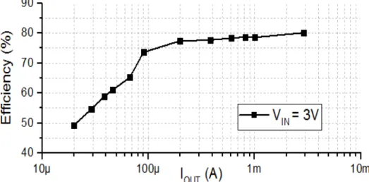
Figure 4.18 shows the VCR and PCE of the active rectifier with the proposed technique without the adaptive delay compensation technique while the input voltage changes from 3V to 12V. The minimum VCR value of the delay-compensated active rectifier is about 0.88 at Vin = 3V, and the maximum VCR value is above 0.96 at Vin = 12V. The VCR and PCE of an active delay-compensated rectifier when the load resistance is varied are shown in Figure 4.19.
Bootstrap-capacitor-less DCM-VOT buck converter
- Background
- Over architecture
- Building blocks
- Proposed high-side driver (MPC level shifter)
- Proposed low-side compensator (DOCC)
- Variable-on-time generator
- High voltage bandgap reference
- Linear regulator
- Measurement results
Before the Vinit_supply reaches the desired voltage, the initialization circuit limits the operation of the converter control circuit. A comparison of the power consumption of MPC level shifters at 10% and 5% duty cycle is shown in Fig.4.27. The conduction loss of the low-side diode in the converter is a factor that reduces the PCE.
The on-time of VOT is determined by f (Vin-Vout), where Vin is the converter input voltage, Vout is the converter output voltage. A voltage reference circuit for the linear regulator and the converter control circuit operates before the other circuits, using the converter input voltage as the power source. The end of 1. bandgap reference circuit is used as voltage supply of 2nd bandgap reference circuit.
When the output of the converter is stabilized and the output of the converter becomes equal to the output voltage of the linear regulator, the linear regulator is disabled. Fig. 4.41 is a WPT configuration measurement setup to verify the operation of the converter in a noisy environment. Measured steady-state waveforms for the converter when VDDH is 3V: (a) IOUT = 660uA, and (b) IOUT=3mA.
Je, "A CMOS rectifier with a cross-coupled latched comparator for wireless power transfer in biomedical applications," IEEE Transactions on Circuits and Systems II," vol. McDannold, "Intermediate range wireless power transfer with segmented coil transmitters for implantable heart pumps", IEEE Trans Bien, “Tracking optimal efficiency of magnetic resonance wireless power transfer system for biomedical capsule endoscopy”, IEEE Trans.
Liang, “An inductive power transfer system with high-Q resonant tank for mobile device charging,” IEEE Trans. Ki, “Wireless Power Transfer System Using Primary Equalizer for Coupling- and Load-Range Extension in Bio-Implant Application”, IEEE Int. Bien, “Tracking optimal efficiency of wireless magnetic resonance energy transfer system for biomedical capsule endoscopy,” IEEE Trans.
Je, “High-efficiency wireless power transfer for biomedical implants by optimal resonant charge transformation,” IEEE Trans. Je, "A CMOS Rectifier with a Cross-Coupled Latched Comparator for Wireless Power Transfer in Biomedical Applications", IEEE Transactions on Circuits and Systems II, Vol. Bien, “Tracking optimal efficiency of wireless magnetic resonance energy transfer system for biomedical capsule endoscopy,” IEEE Transactions on Microwave Theory and Techniques, vol.