I declare that this report entitled “DESIGN OF DIRECT MEMORY ACCESS MODULE FOR 32-BIT RISC32 PROCESSOR” is my own work, except those mentioned in the references. Mok Kai Ming and Dr Chang Jing Jing for his constant supervision, suggestions for the project, and all the encouragement and life lessons he had given me during my years of study. I would also like to thank my loving family for giving me the support and financial help I need during my years of study.
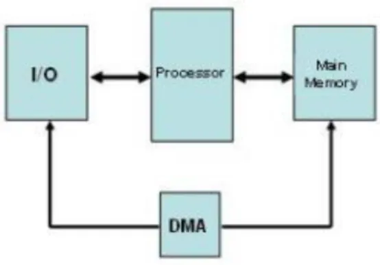
The project is about the design and implementation of a direct memory access (DMA) specifically for the Reduced Instruction Set Computer (RISC-32) processor. A partition level diagram is drawn to help users understand what is inside the DMA controller.
Introduction
- Background Information
- Direct Memory Access (DMA)
- MIPS
- Bus
- Motivation
- Problem Statement
- Project Scope
- Project Objectives
- Impact, Significance, and Contribution
Additionally, an interrupt service routine (ISR) for handling all interrupt requests generated by the DMA controller will be developed and then integrated into the existing exception handler of the RISC32 pipeline processor. Some MIPS test programs will also be written to test the functions of the DMA controller after integration, as well as to verify the correctness of the ISR execution. This includes micro-architecture modeling and verification of the DMA controller using the Verilog language.
This includes the development of an interface between the DMA controller and the RISC32 based on the I/O memory mapping technique. When the project is implemented in the RISC32 MIPS environment, it can significantly increase the research speeds of future research work due to the functionality of the DMA controller.
Literature Review
Overview of Direct memory access (designed by Ahmed, 2019)
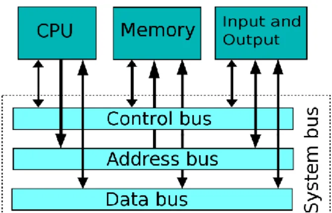
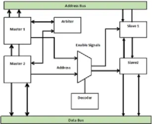
- Advanced Microcontroller Bus Architecture (AMBA)
- Pin description of DMA (designed by Ahmed, 2019)
- Block diagrams of Direct memory access (designed by Ahmed, 2019)
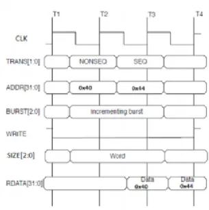
- Timing Diagram of DMAC
It will be synchronous once it is connected to the control unit from several masters, so that they can be accessed in one control unit. It is a low-performance bus designed only to connect the peripherals on the System on chip (SoCs). This bus is the AHB master to address one of the slaves of APB system when the APB and AHB are connected.
This bus only connects the master and slave and is thus placed on the edge side. To build and deploy this AMBA design so that it works as intended, the Verilog hardware descriptive language (HDL) is used.
Overview of Direct memory access (designed by Jagtap, 2017)
Multichannel DMA controller
Block diagrams of the DMAC
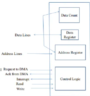
A series of commands will be sent from the processor when a huge amount of data needs to be transferred. The buses will be taken over by the DMA once the procedure has started and can only be stopped when an acknowledgment signal is sent from the DMA to the processor indicating the completion of the process. In this current design, efficient communication is the main focus between the memory and the processor with various commands from the controller, which gives more flexibility and versatility to the design.
As mentioned above, an interrupt will occur as soon as it senses any data to be transferred from the processor or memory or vice versa. It stops its current task in hand so that it can give DMAC permission to control all buses after all the requirements are met: handshake, recognition, opcode data, etc.
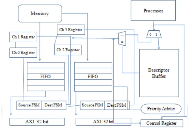
Datapath of proposed DMA
With this, the DMAC is implemented in the computer architecture and is shown in the figure below. This design consists of 4 channels, arbitration module, channel registers, 3 AXI masters, one AXI slave, asynchronous FIFO buffers. Again the DMAC consists of 4 channels and each one does a specific type of data transfer, for example the first channel has to transfer a type of data which can be addresses and the second channel is for normal data transfer, then they will do as told and must not overlap , which would cause confusion at the receiving end.
Although four AXI masters are mentioned, there is only one associated with the AXI protocol. The two other AXI masters can be connected to the external memory or to the Double Data Rate (DDR). There are two modes that this DMA controller can run in: the first is data transfer mode and the second is descriptor transfer mode.
The first is when the DMA controller transfers a huge load of data and then a different priority channel is selected. While in the second mode, tasks are sent to the channel descriptor by the processor ahead of schedule. After this happened, the arbitration scheme would select the highest priority channel, meaning that the transfer that occurs first (data transfer) in the data description will load the work registers and execution of related data transfer will be started.
Thus the data is transferred to the DMA controller without the intervention and involvement of the processor.
Proposed Method/ Approach
- Methodologies and General Work Procedures
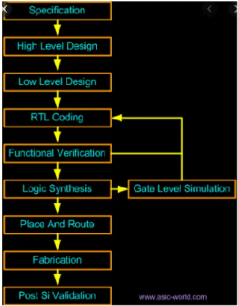
- RTL Design Flow
- Micro-architecture Specification
- RTL Modelling and Verification
- Logic synthesis for FPGA
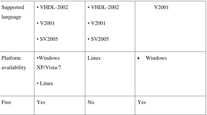
- Design Tools
- ModelSim Student edition-x64 10.5
- Xilinx Vivado Design Suite
- PCSpim
- Implementation Issues and Challenges
- Timeline
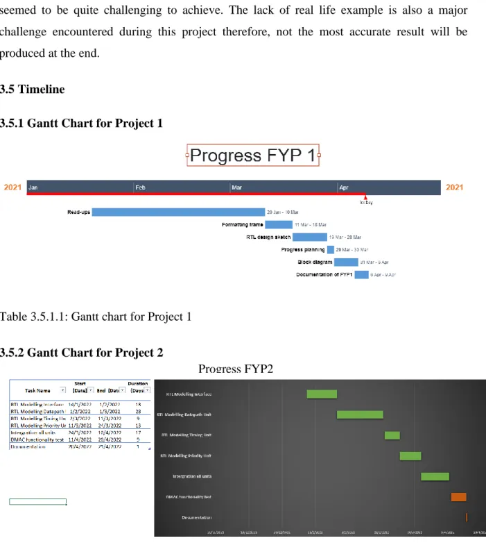
- Gantt Chart for Project 1
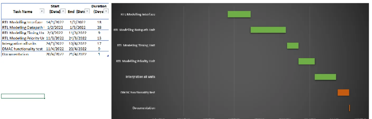
- Gantt Chart for Project 2
This part of the project will give a detailed description of the internal design of the DMA controller. The internal design of the DMA controller will be described in detail and also design-specific technical information will be provided so that the design is as accurate as possible. After the microarchitecture specification is figured out, the RTL coding of the DMA controller can begin.
During the project development process, the design does not meet the requirements of the DMA controller; the design flow would have to be repeated until everything is done right. After the DMA controller unit has been fully verified for its functionality, the model would be ready for logic synthesis that requires translation of RTL code to gate-level representation. Based on the result, the port level unit should be re-verified for its functional correctness.
Each of the steps mentioned above, from building the design to the physical model, would require both software and hardware tools. Although it only offers a free license for the student version only instead of the full version, it is already sufficient as we do not need the full functionality of the software for this current project. We only needed the Verilog language and VHDL, which is available in the student version of the aforementioned simulator.
Configuration of the device is also available which makes it easier for users to complete the tasks. Therefore, this tool will be extremely useful in developing MIPS test program to verify the correctness of the interrupt service routine (ISR). With just the logic analysis, the implementation of the DMA in RISC32 is feasible, with the introduction of clock signals and edge positive sensitive data, a more detailed testing needs to be done.
System Specification
System Overview of Risc32 Pipeline Processor
- RISC32 Pipeline Processor Architecture
- Functionality of RISC32 Pipeline Processor
- Memory Map of the RISC32 Pipeline Processor
Two different modes are applied in the RISC32 pipeline processor, they are called physical and virtual addresses each with its own purposes. Physical address is used to divide physical memory into different things like flash memory, ROM and RAM. 16k bytes User program code Used to store user program codes 128k bytes Table 4.1.3.1: Description of RISC32 pipeline processor memory map.
Chip Interface of the RISC32 Pipeline Processor
- Input Description of the Chip Interface of the RISC32 Pipeline Processor
Pin Function: Input control when used by the CPU to read control registers and output signal used to access data from peripherals during DMA write transfers. Pin Function: Input control when used by the CPU to load information into DMAC and output used to load data to peripherals during DMA read transfer.
Micro-Architecture Specification
- DMA Controller Unit
- Functionality/ Feature of the DMA Controller Unit
- Operating Procedure (External Operation)
- Unit Interface of the DMA controller
- Input Pin Description of the DMA Controller Unit
- Output Pin Description of the DMA Controller Unit
- Input Output Pin Description of the DMA Controller Unit
- Finite State Machine of DMA controller operations
- Design Partitioning of the DMA Controller unit
- Micro-Architecture of the DMA Controller Unit (Block Level)
- DMAC Datapath Unit
- Functionality/Feature of the Datapath Unit
- Block Interface of the DMAC Datapath Unit
- Input Pin Description of the DMAC Datapath Unit
- Output Pin Description of the DMA Controller Unit
- Input Output Pin Description of the DMA Controller Unit
- DMAC Timing and Control Unit
- Functionality/Feature of the Timing and Control Unit
- Block Interface of the DMAC Timing and Control Unit
- Input Pin Description of the Timing and Control Unit
- Output Pin Description of the Timing and Control Unit
- Input Output Pin Description of the Timing and Control Unit
- DMAC Priority Unit
- Functionality/Feature of the Priority Unit
- Block Interface of the DMAC Priority Unit
- Input Pin Description of the DMAC Priority Unit
- Output Pin Description of the DMAC Priority Unit
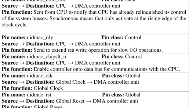
Pin Name: uidmac_clk Pin Class: Global Source → Destination: Global Clock → DMA Controller Device Pin Function: Global Clock. Pin Name: uidmac_rst Pin Class: Global Source → Destination: Global Reset → DMA Controller Device Pin Function: Global Reset. Pin Name: uidmac_aen Pin Class: Control Source → Destination: DMA Controller Device → Address Bit Lock.
Pin Name: uidmac_memw_n Pin Class: Control Source → Destination: DMA Controller Unit → Memory Storage Unit. Pin Name: uidmac_eop_n Pin Class: Control Source → Destination: DMA Controller Unit ↔ On-Chip Transistor. Pin Name: bidmac_ctrl_time_hold_ack Pin Class: Control Source → Destination: CPU → bidmac_ctrl_time.
Pin Name: bidmac_ctrl_time_chipslt_n Pin Class: Control Source → Destination: CPU → bidmac_ctrl_time. Pin Name: bidmac_ctrl_time _clk Pin Class: Global Source → Destination: Global Reset → bidmac_ctrl_time. Pin Name: bidmac_ctrl_time _aen Pin Class: Control Source → Destination: bidmac_ctrl_time → address bitlock.
Pin Name: bidmac_ctrl_time _memr_n Pin Class: Control Source → Destination: bidmac_ctrl_time → Memory Storage Unit. Pin Name: bidmac_ctrl_time _memw_n Pin Class: Control Source → Destination: bidmac_ctrl_time → Memory Storage Unit. Pin Name: bidmac_ctrl_time _iord_n Pin Class: Control Source → Destination: bidmac_ctrl_time → bidmac_dp.
Pin name: bidmac_ pr _dack[3:0] Pin class: data source → Destination: bidmac_ctrl_time → address bit lock. Pin name: bidmac_ pr _holdrq Pin class: data source → Destination: bidmac_ctrl_time → Memory storage unit.
VERIFICATION SPECIFICATION AND STMULATION RESULT 63
SYNTHESIS AND IMPLEMENTATION
DMA Interface With RISC32 Processor
Timing Waveforms of the DMA Processes
Conclusion and Future Work
Conclusion
Future Work
Li, "VLSI implementation of a high-performance 32-bit RISC microprocessor," in Communications, Circuits and Systems and West Sino Exhibitions, IEEE International Conference 2002, 2002. Faculty of Information and Communication Technology (Kampar Campus), UTAR . input CS_N, input DB, input ADDR_L, output ADDR_U. Faculty of Information and Communication Technology (Kampar Campus), UTAR .. input RESET, . input VALID_DREQ0, input VALID_DREQ1, input VALID_DREQ2, input VALID_DREQ3, output hrq, . exit ldCurrAddrTemp, exit ldCurrWordTemp, exit enCurrAddr, exit ldTempCurrAddr, exit ldTempCurrWord, Exit Program, . exit validDACK );. input CLK, input RESET, input hrq, . valid inputDACK, output VALID_DREQ0, output VALID_DREQ1, output VALID_DREQ2, output VALID_DREQ3.
Completed DMA interface outsourcing study, started designing RTL model for DMA interface using modelsim SE. RTL modeling for Datapath unit, Block interface, pin description and functionality, diagram of some register commands and FSM. RTL modeling to describe the pinouts and functionality of the control unit, some register command diagrams and the FSM.
RTL modeling to describe priority unit pins and functionality, diagram of some register commands and FSM. Form Title: Supervisor Comments on Originality Report Generated by Turnitin for Final Year Project Report Submission (for Undergraduate Programs). Final Year Title Direct Memory Access Module Project Design for 32-bit RISC32 Processor.