This book lists the problems at the end of the chapter for each of the tutorials in the book "CMOS Integrated Circuit Simulation with LTspice" (3rd Edition, 2020, also published by Bookboon) and provides solutions to the problems. The exercises are taken from 'CMOS Integrated Circuit Simulation with LTspice' and the references to figures in the exercises are to figures from this book. You can also download the model files from the webpage of 'CMOS Integrated Circuit Simulation with LTspice'.
The model files that include the speed parameters are included in the transistor models file, which can be downloaded from the 'CMOS Integrated Circuit Simulation with LTspice' website.
Resistive Circuits
For the circuit shown above, determine the value of the voltages v1 and v2 and the current ix. For the circuit shown above, find the value of gain Avoc that gives an output power inRL of 1 W when the signal voltage vs is 50 mV. The value of one of the resistors and the conductance value of the voltage-controlled current source are unknown.
In the LTspice schematic shown below, we define Rx as a parameter and the conductance of the voltage controlled current source is '{1/(3*Rx)}'.
Circuits with Capacitors and Inductors
What initial value of the input voltage fin will result in an average value of 0 V for the output voltage vo. From the plot of the output voltage, a 'Ctrl-left-click' on the label 'V(vo)' shows an average value of. For finding the time required for VO to reach 90% of the final value, we use the second '.meas' directive shown in the LTspice schematic.
To find precise values of the output voltage and ripple we can use the '.meas' guidelines shown in the schematic.
MOS Transistors
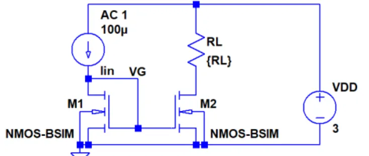
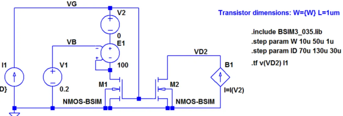
The bias values and small signal parameters are given in the error log ('Ctrl-L') from this simulation, see below where the desired parameters are underlined. Find the ID of the bias current and the small-signal parameters gm,gmbandgdsforL=1 µm and forL=5 µm at the bias point. To find the bias current ID and the small-signal parameters gm, gmb, and gds for L=1 µm and for L=5 µm at the bias point for VGS=1.5 V, VDS=2.0 V, and VSB=0 V, we specify the value using a '.param' directive (shown as comments in the LTspice schema), while changing the '.step param' directive to a comment.
For finding ∂iD/∂vSDforVSG=1.5 V,VBS=0 V and VSD=2.0 V, the iIDis derivative is plotted as shown in the figure below. Simulate and plot the input characteristics (ID vs. VSG) and output characteristics (ID vs. VSD) using the BSIM model and the Shichman-Hodges model with parameters estimated from the simulation of the small-signal parameters at the bias point. The simulations result in the characteristics shown below with the green curves for the BSIM3 model and the blue curves for the Shichman-Hodges model.
From the gm and gds plots, find the maximum drain current at which the transistor is in the active region for each of the three channel width values. From the curves, we find the following maximum values of the drain current for which the transistor is in the active region:. In the active region, gmis is found from gm=. showing the square root dependence of ID, see Eq. 3.8) in "CMOS Integrated Circuit Simulation with LTspice".
In the triode region gmis have been found of. showing that gm does not depend on ID, see Eq. 3.11) in 'CMOS Integrated Circuit Simulation with LTspice'. Forgds we note that in the active region, . showing that gd is independent of W and increases linearly with ID, see Eq. 3.9) in 'CMOS Integrated Circuit Simulation with LTspice'.
Basic Gain Stages
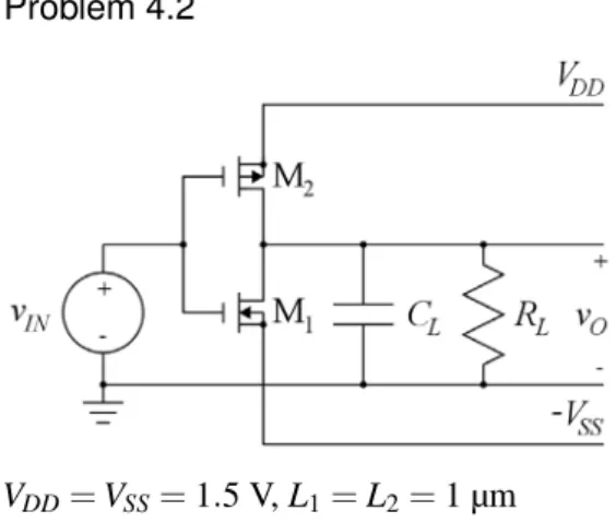
With W1=6.5 µm and W2=21 µm, we run an '.op' simulation to verify the output voltage bias value and a '.tf' simulation to verify the gain. To find the low frequency gain when the RL is removed, we run a '.tf' simulation where the RL is disconnected. To verify that the '.ac' simulation runs from a reasonable bias point, also whenRL=∞, an '.op'.
To find the channel widthW1 we run an '.op' simulation on a single NMOS transistor with gate, source, drain and bulk connected to voltages resulting in the highest value of output voltage. To find the open-circuit voltage gain and output resistance for an input bias voltage of 0 V, we run a '.tf' simulation with 'RL' disconnected. For this we use the directive '.meas VINbias when v(VO)=0' (shown as a comment in the LTspice schematic) and run a '.dc' simulation.
Use a small step size (1 mV) for the '.dc' simulation to get a fairly accurate result from the '.meas' directive. To verify the bias point, we run an '.op' simulation with a dc value of VIN specified to 708.209 mV. With the bias point in place, the small signal gain Avoc and output resistance ro at low frequencies are found from a '.tf' simulation with V(VO) as the output and VIN as the source.
For finding the small-signal resistance rx to ground from the node xbetween the source of M2 and the drain of M1, we run a '.tf' simulation with V(Vx) as the output and VInas the source. To verify the bias point, we perform an '.op' simulation with a dc value of VIN specified to 693.684 mV. For finding the small-signal resistance rx to ground from the node xbetween the source of M2 and the drain of M1, we run a '.tf' simulation with V(Vx) as the output and VIN as the source.
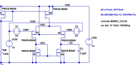
Define the AC amplitudes of 'VCM', 'V1', 'V2' and 'VDD' so that the '.ac' simulation shows the differential gain and compare your simulation with Fig.
Hierarchical Design
We can also use the directive '.meas dc VB when v(Vo)=1.5' in the schematic to verify the value of VB. The error log file opens automatically after running the simulation because some floating nodes in the circuit generate error messages. With the '.meas' directives shown in the schematic, the error log reports a low-frequency gain of 13.9794 dB and a bandwidth of 30.6363 MHz.
Again, the error log file opens automatically after running the simulation due to some floating nodes in the circuit. By using the 'Edit' and 'Draw' commands in the symbol editor, the symbol can be modified to look like the following figure. When you click 'File → Save', the symbol is saved in the same folder as the subcircuit schematic file.
The passband gain and bandwidth can also be found from the '.meas' directives shown in the LT-spice scheme. Find the passband gain, the frequency at which the gain has its maximum magnitude and the magnitude of the peak in the frequency response. The peak and the frequency of the peak can also be found from the '.meas' directives shown in the schematic.
Inserting these values as parameters for the filter block BP2.asc from Problem 5.3 results in the following LTspice schema. By using the 'Edit' and 'Draw' commands in the symbol editor, the symbol can be modified to look like the symbols shown above.
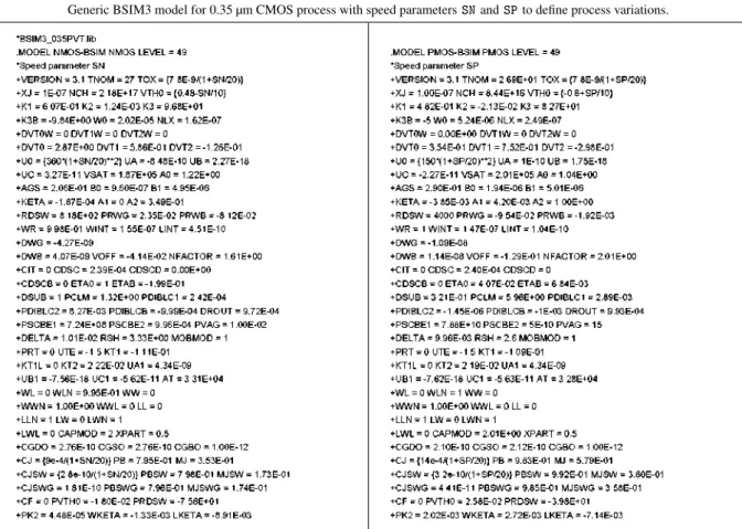
Process and Parameter Variations
To show both temperature variations and process parameter variations, we step both temperature and speed parameters as shown in the following schematic. To ensure a correct dc bias point for the '.ac' simulation in all process angles we apply a dc feedback as shown in the figure below (Fig. Rather than using the pointers to find the process angles , we use the results of the '.measure' instruction found in the following error log file ('Ctrl-L').
The results can also be displayed graphically by right-clicking in the error log and selecting 'Plot .step'ed .meas data'. The schematic with these changes is shown in the following figure, along with a plot of the temporary simulation and the results of the error log file. We can find the unity gain frequency from the graph resulting from an '.ac' simulation, but it is easier to use the '.meas' directive in the schematic to calculate the process angular values of the unity gain frequency.
The results from the '.meas' directive are in the error log from the '.ac' simulation and we find that the worst possible corner is the combination of a low supply voltage and a high temperature. The process corners can also be displayed graphically by right-clicking in the error log file and selecting. For a Monte Carlo simulation with 50 simulations, a step counter parameter N must be defined as shown in the following scheme.
The simulation error log file provides the calculated values of unity gain bandwidth for each of the 50 steps in the Monte Carlo simulation. By right-clicking in the error log and selecting 'Plot .step'ed .meas data' the results can also be plotted graphically, as also shown in the following figure.
Importing and Exporting Files
The simulation is run directly from the netlist file in LTspice using the command 'Simulate → Run' (or . 'Ctrl-R'), and in the plot window that opens, the traces to be plotted are selected using ' Plot Setup → Add Trace' (or 'Ctrl-A'). Place the differential pair in a test bench as shown in the figure below and find the low-frequency differential gain and the −3 dB frequency for the differential gain. Placing the cursor in the '.subckt' line and right-clicking generates a symbol and using the graphical symbol editor it can be changed to the symbol shown below.
To ensure portability of the symbol, you can save the symbol (difpair.asy) and the netlist file (difpair.net) in the same folder as the schematic of your testbench. Also use the command 'Edit → Attributes → Edit Attributes' in the symbol editor to just specify 'difpair' as the 'ModelFile' rather than the full pathname to the file. The low-frequency differential gain and the -3 dB frequency for the differential gain can also be found using the '.meas' guidelines shown in the schematic.
The subcircuit is also renamed to 'difpairw' with a corresponding symbol as shown in the following figure. In the following figure, separate plot windows are used for the gainAd and the -3 dB frequency BW. Find the input bias voltage VIN that results in the maximum absolute value of the small-signal gainvout/vin and find the maximum absolute value of the gain.
Also find the small-signal output resistance of the amplifier for the input bias that results in the maximum absolute value of the gain. The '.dc' simulation specified in the schematic results in the following plot of vOUT and the small-signal gainvout/vin.