Devinder Singh is currently working as an Assistant Professor at Amity School of Applied Sciences, Amity University, Lucknow, India. With the introduction of advanced methodologies, important methods for crystal structural analysis in the field of electron crystallography have been discovered.
Introduction
This software-based method is called rotational electron diffraction (RED), which is able to overcome the drawbacks and reduce the dynamic effects [8]. A complex pseudo-decagonal quasicrystal approximation Al37(Co,Ni)15.5 solved by the rotational electron diffraction (RED) method.
Transmission electron microscope 1 Preferred orientation and texture
- Dislocation
- Kikuchi patterns
- Twinning
- Core-shell nanoparticles
- Carbon nanotubes
Consequently, incomplete sectors of the rings were patterned due to preferred orientation in the crystal structure. TEM images of nanostructured alloys and corresponding SAEDPs of the two samples demonstrated in Figure 2 .
Transmission electron microscopy in the study of Al/BN Nanocomposite
Phase evaluation
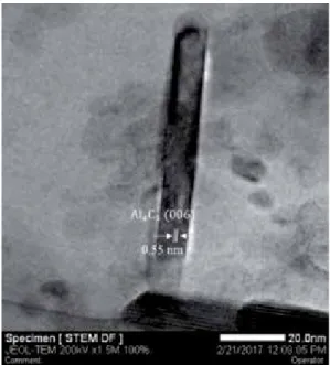
EDS analysis as a valid technique in TEM is used to characterize the insitu phases of Al4C3 in the microstructure of Al-2 wt. Therefore, the AlN phase was created by the reaction of Al and N in the hot extrusion process.
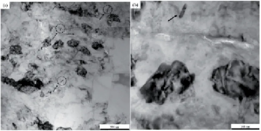
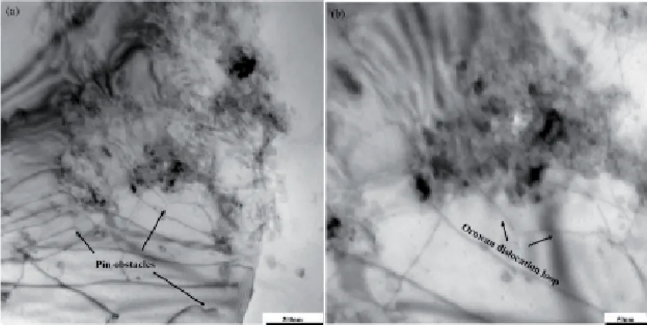
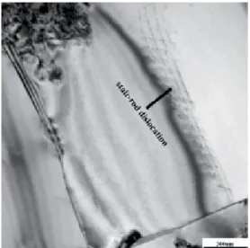
Dislocation
Microstructural observations
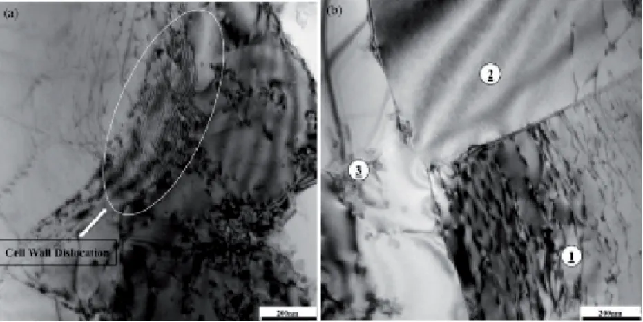
As can be seen, the matrix consists of recrystallized nano/ultrafine grains with high-angle boundaries and a density of free dislocations. Low-angle grain boundary image surrounded by high-angle grain boundaries (higher magnification views in Fig. 19(b) ).
Conclusions
Mechanical properties of Al/BN nanocomposites produced by planetary ball milling and conventional hot extrusion. Quasicrystals that are projections of non-cubic lattices (e.g., Elser-Sloane tiling as a projection of the E8 lattice in4) are more restrictive, and some modifications have been made to the cut and project method to correctly calculate their tilings and empires [18].
Empires in quasicrystals
Methods for generating empires
The cut-and-project method offers the most generality and has been used to calculate realms for the Penrose tiling and other quasicrystals that are projections of cubic lattices[16, 17]. The cut-and-project formalism can also be modified to compute the space of all tiles allowed by a given patch, in which the set of constrained tiles of the patch's realm is exactly the mutual intersection of all tiles containing that patch [15].
Empires in 2D
Recently, the cut-and-project technique [14, 15] – where the geometry of convex polytopes comes into play – has been implemented into the most efficient method of computing empires [16]. In this chapter, we review the nonlocal properties of quasicrystals and the studies done to create and analyze empires, and discuss some of the findings and their possible implications.
Empires in 3D
The forced tiles that are at a distance from the emperor make up the non-local part of the empire. In Figure 2 we show the empires and the possibility space of the fivefold symmetric vertices, S5 (the star) and S (the sun) [16].
Quasicrystal dynamics
The tilings of this quasicrystal are all rhombohedrons, and the vertex configurations are analogous to those of the Penrose tiling. In Figure 4 one can see the K-vertex type and 2D representation of the nearest neighbors in the perpendicular space we considered [17].
Empires and higher dimensional representations
Solar configurations surrounded by the five orientations of the K-type vertex plotted in two different colors corresponding to the two distinct regions in perpendicular space from which these configurations are projected. This also applies to the case in which the solar configurations are projected from the other region into perpendicular space.
Conclusions
The K vertex patch tiles closest to the center—the sun—remain uncovered by the realms of the other suns. For various vertex configurations, we analyzed their realms—the nonlocal distribution of their forced tilings—relative to the higher dimensional representation.
Materials and experimental procedure
This helps us gain a deep understanding of the relationships between quasicrystals and their approximate phases. Reproduced with permission from the International Union of Crystallography (https://scripts.iucr.org/cgi-bin/paper?HE5621) [41].
Structure analysis of PD2 and PD1 quasicrystal approximants 1 RED data processing
After each refinement step, the stability of the atoms in the structure model was checked. Reproduced with permission from the International Union of Crystallography (https://scripts.iucr.org/cgi-bin/paper?jo5016) [42].
Texture formation by intense rolling
Rolling procedure
Let's look at how to control the crystallographic structure of metals and metal alloys through the technology of plasticity in metal forming and surface treatment. These previous studies proved that grain size as well as crystallographic structure should be significantly controlled by the material processing other than the shearing process in metal forming.
Microstructure evolution by intense rolling
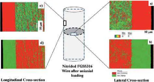
In the present chapter, the crystallographic structure evolution of stainless steel during the rolling, the piercing and the plasma nitriding at 623 K for 14.4 ks is first described to deduce the mechanism of microstructure evolution during metal forming and material processing. Next, the uniaxial loading test of plasma nitride work at 623 K is performed to investigate the possibility of further microstructure evolution during posterior metal forming.
Controlled crystallographic structure by intense rolling
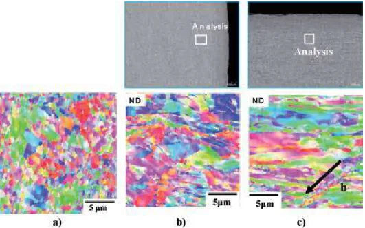
In the following, AISI304 plate was used as a work to reduce its thickness from 10 mm down to 1 mm by intense rolling. In addition to the stress-induced phase transformation in Figure 3, the intense rolling has a lot of influence on the crystallographic structure in AISI304.
Crystallographic change by piercing
Microstructure evolution by piercing
Phase mapping in Figure 5d–f reveals that these process-affected regions only correspond to the martensitic phase [24]. It should be noticed that the volume of the martensite phase caused by the deformation becomes larger in Figure 6f than that in Figure 6e.
Controlled crystallographic structure by piercing
When punching the AISI316L sheet, the strain-induced martensitic phase almost did not occur along the cutting plane; no martensitic phase was present in Figure 7a. As a result, the process-affected zone area in AISI316L becomes larger along the cutting plane in Figure 7a than in AISI304 in Figure 7b [28].
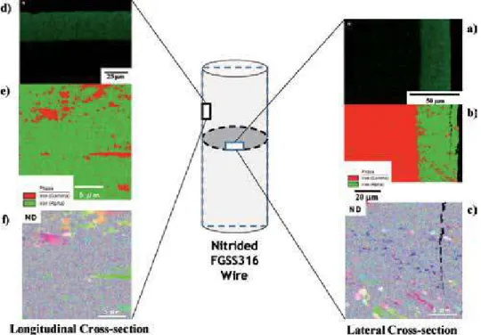
Nanostructuring by low temperature plasma nitriding
- Low temperature plasma nitriding
- Microstructure evolution by inner nitriding in depth
- Microstructure evolution in FGSS316 wires
- Controlled crystallographic structure by plasma nitriding
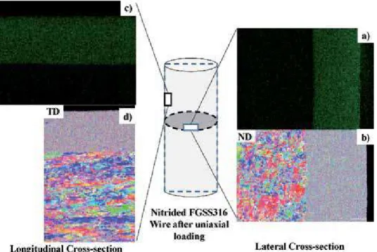
- Uniaxial loading procedure
- Microstructure evolution during uniaxial loading at RT
The microstructure as well as the phase in the matrix under the NFE is modified by this uniaxial loading. The phase transformation and formation of the bundle microstructure in the above is reflected in the crystallographic structure after uniaxial loading.
Discussion
The microstructure in the nitrided layer is also influenced by uniaxially applied plastic stresses. This in situ refinement of the grain structure in the nitrided layer reflects on the hardness profile.
Conclusion
The study of photochemical and photophysical properties of heterocyclic compounds has received much attention during the last decade. The study of photochemical and photophysical properties of heterocyclic compounds has received much attention during the last decade.
Structural commentary
The influence of the presence of nitrogen atoms on the fluorescence spectral maxima of aromatic molecules is our interest, including comparison of the spectra in polar and non-polar solvents. to understand the characteristics of chemical bonding in molecules from the topological analysis of electron densities [4] and various electrostatic properties of molecules. The time-dependent density functional theory (TD-DFT)/quantum theory of atoms in molecules (QTAIM)/orbital analysis and molecular electrostatic potential (MESP) theoretical calculations were also applied.
Supramolecular features
Luminescent properties
The studied compound was found to be fluorescently active in solution at room temperature. a) Partial view of the packing in phh showing the O▬H⋯O, O▬H⋯N, C▬H⋯O and C▬H⋯N hydrogen bonds. The spectra clearly reveal that the emission originates from a π-π* charge transfer excited state due to the presence of N atoms.
Theoretical analysis
TD-DFT absorption spectra
Fluorescence spectra of phh in polar and nonpolar solvents. temperature showing an intense blue fluorescence with high fluorescence quantum yield independent of the excitation wavelength in different solvents. Time-dependent density functional theory calculations were performed on this compound, with the aim of identifying the nature of the electronic transitions.
AIM topological analysis
From Figure 4 we observe two absorption peaks located at λ= 225 and 190 nm; the absorption bands correspond to H1 to L+3 and H3 to L+2, respectively; and these transitions are affected to aπ-π* transition.
Orbital analysis and molecular electrostatic potential
The energy diagram of the molecular orbitals obtained by DFT approach for part B of compound phh is shown in Figure 6. The molecular electrostatic potential is a very important element for illustrating and visualizing the charge region variability and makes it possible to identify the electrophilic and nucleophilic attack sites as well as the hydrogen bonding interactions [18–21].
Crystallization
Programmes
Refinement
On a Perkin-Elmer spectrometer, infrared spectra were recorded at room temperature in a range of 500-4000 cm 1 .
Conclusion
Nevertheless, it is difficult to obtain such information about the motion of the dislocation moving through the forest dislocations and overcoming the weak obstacles such as impurities during bulk plastic deformation. Internal friction measurements deal with the motion of the dislocation that vibrates away from the weak barriers between two forest dislocations [31].
Combination method of strain-rate cycling tests and the Blaha effect measurement
Dopant ions are expected to cause solidification due to the motion of dislocations, which at low temperature is hindered by defects around them. This chapter is concerned with the energy supplied by thermal fluctuations when dopant ions are overcome by dislocation through thermal activation during plastic deformation of crystals.
Model overcoming the thermal obstacle by a dislocation
Within the first plateau region of the relative curve (that is, region 1 in Fig. 3), the application of low voltage amplitude oscillation cannot affect the average length of dislocation segments (l ¯) and l is assumed to remain constant. Within the first plateau region of the relative curve (that is, region 1 in Fig. 3), the application of low voltage amplitude oscillation cannot influence the average length of dislocation segments (l ¯ ), and l ¯ is assumed to remain constant.
Relation between the effective stress due to impurities on activation volume
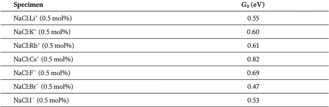
Figure 5(b) corresponds to typical force-distance curve for short-range barrier below that in Figure 4. Relationship between τp and activation volume (V) for NaCl:Rb+ (0.5 mol%) (reproduced from Ref. [58] with permission of the publisher). where k is the Boltzmann constant and T is the absolute temperature.
Conclusions
Variation of interaction energy (G0) between dislocation and dopant ion with defect size (reproduced from Ref. [58] with permission from the publisher). Experimental determination of the force-distance coupling for the interaction between a dislocation and a solute atom.